EP2320526A1 - Abschirmungsgehäuse und Verbinder damit - Google Patents
Abschirmungsgehäuse und Verbinder damit Download PDFInfo
- Publication number
- EP2320526A1 EP2320526A1 EP20100251851 EP10251851A EP2320526A1 EP 2320526 A1 EP2320526 A1 EP 2320526A1 EP 20100251851 EP20100251851 EP 20100251851 EP 10251851 A EP10251851 A EP 10251851A EP 2320526 A1 EP2320526 A1 EP 2320526A1
- Authority
- EP
- European Patent Office
- Prior art keywords
- receiving portion
- shield case
- cover
- folded
- top plate
- Prior art date
- Legal status (The legal status is an assumption and is not a legal conclusion. Google has not performed a legal analysis and makes no representation as to the accuracy of the status listed.)
- Granted
Links
- 238000005192 partition Methods 0.000 claims description 9
- 238000004519 manufacturing process Methods 0.000 abstract description 2
- 230000003014 reinforcing effect Effects 0.000 description 17
- 238000000465 moulding Methods 0.000 description 6
- 238000005476 soldering Methods 0.000 description 6
- 238000005520 cutting process Methods 0.000 description 5
- 239000002184 metal Substances 0.000 description 5
- 239000000470 constituent Substances 0.000 description 2
- 230000008030 elimination Effects 0.000 description 2
- 238000003379 elimination reaction Methods 0.000 description 2
- 230000004907 flux Effects 0.000 description 2
- 239000000463 material Substances 0.000 description 2
- 230000013011 mating Effects 0.000 description 2
- 239000011347 resin Substances 0.000 description 2
- 229920005989 resin Polymers 0.000 description 2
- 229910000679 solder Inorganic materials 0.000 description 2
- 238000005452 bending Methods 0.000 description 1
- 238000000151 deposition Methods 0.000 description 1
- 238000000034 method Methods 0.000 description 1
- 230000004048 modification Effects 0.000 description 1
- 238000012986 modification Methods 0.000 description 1
Images


Classifications
-
- H—ELECTRICITY
- H01—ELECTRIC ELEMENTS
- H01R—ELECTRICALLY-CONDUCTIVE CONNECTIONS; STRUCTURAL ASSOCIATIONS OF A PLURALITY OF MUTUALLY-INSULATED ELECTRICAL CONNECTING ELEMENTS; COUPLING DEVICES; CURRENT COLLECTORS
- H01R13/00—Details of coupling devices of the kinds covered by groups H01R12/70 or H01R24/00 - H01R33/00
- H01R13/648—Protective earth or shield arrangements on coupling devices, e.g. anti-static shielding
- H01R13/6485—Electrostatic discharge protection
-
- H—ELECTRICITY
- H01—ELECTRIC ELEMENTS
- H01R—ELECTRICALLY-CONDUCTIVE CONNECTIONS; STRUCTURAL ASSOCIATIONS OF A PLURALITY OF MUTUALLY-INSULATED ELECTRICAL CONNECTING ELEMENTS; COUPLING DEVICES; CURRENT COLLECTORS
- H01R27/00—Coupling parts adapted for co-operation with two or more dissimilar counterparts
- H01R27/02—Coupling parts adapted for co-operation with two or more dissimilar counterparts for simultaneous co-operation with two or more dissimilar counterparts
-
- H—ELECTRICITY
- H01—ELECTRIC ELEMENTS
- H01R—ELECTRICALLY-CONDUCTIVE CONNECTIONS; STRUCTURAL ASSOCIATIONS OF A PLURALITY OF MUTUALLY-INSULATED ELECTRICAL CONNECTING ELEMENTS; COUPLING DEVICES; CURRENT COLLECTORS
- H01R13/00—Details of coupling devices of the kinds covered by groups H01R12/70 or H01R24/00 - H01R33/00
- H01R13/646—Details of coupling devices of the kinds covered by groups H01R12/70 or H01R24/00 - H01R33/00 specially adapted for high-frequency, e.g. structures providing an impedance match or phase match
- H01R13/6461—Means for preventing cross-talk
-
- H—ELECTRICITY
- H01—ELECTRIC ELEMENTS
- H01R—ELECTRICALLY-CONDUCTIVE CONNECTIONS; STRUCTURAL ASSOCIATIONS OF A PLURALITY OF MUTUALLY-INSULATED ELECTRICAL CONNECTING ELEMENTS; COUPLING DEVICES; CURRENT COLLECTORS
- H01R13/00—Details of coupling devices of the kinds covered by groups H01R12/70 or H01R24/00 - H01R33/00
- H01R13/646—Details of coupling devices of the kinds covered by groups H01R12/70 or H01R24/00 - H01R33/00 specially adapted for high-frequency, e.g. structures providing an impedance match or phase match
- H01R13/6473—Impedance matching
-
- H—ELECTRICITY
- H01—ELECTRIC ELEMENTS
- H01R—ELECTRICALLY-CONDUCTIVE CONNECTIONS; STRUCTURAL ASSOCIATIONS OF A PLURALITY OF MUTUALLY-INSULATED ELECTRICAL CONNECTING ELEMENTS; COUPLING DEVICES; CURRENT COLLECTORS
- H01R24/00—Two-part coupling devices, or either of their cooperating parts, characterised by their overall structure
- H01R24/28—Coupling parts carrying pins, blades or analogous contacts and secured only to wire or cable
- H01R24/30—Coupling parts carrying pins, blades or analogous contacts and secured only to wire or cable with additional earth or shield contacts
-
- H—ELECTRICITY
- H01—ELECTRIC ELEMENTS
- H01R—ELECTRICALLY-CONDUCTIVE CONNECTIONS; STRUCTURAL ASSOCIATIONS OF A PLURALITY OF MUTUALLY-INSULATED ELECTRICAL CONNECTING ELEMENTS; COUPLING DEVICES; CURRENT COLLECTORS
- H01R12/00—Structural associations of a plurality of mutually-insulated electrical connecting elements, specially adapted for printed circuits, e.g. printed circuit boards [PCB], flat or ribbon cables, or like generally planar structures, e.g. terminal strips, terminal blocks; Coupling devices specially adapted for printed circuits, flat or ribbon cables, or like generally planar structures; Terminals specially adapted for contact with, or insertion into, printed circuits, flat or ribbon cables, or like generally planar structures
- H01R12/70—Coupling devices
- H01R12/71—Coupling devices for rigid printing circuits or like structures
- H01R12/72—Coupling devices for rigid printing circuits or like structures coupling with the edge of the rigid printed circuits or like structures
- H01R12/722—Coupling devices for rigid printing circuits or like structures coupling with the edge of the rigid printed circuits or like structures coupling devices mounted on the edge of the printed circuits
- H01R12/725—Coupling devices for rigid printing circuits or like structures coupling with the edge of the rigid printed circuits or like structures coupling devices mounted on the edge of the printed circuits containing contact members presenting a contact carrying strip, e.g. edge-like strip
-
- H—ELECTRICITY
- H01—ELECTRIC ELEMENTS
- H01R—ELECTRICALLY-CONDUCTIVE CONNECTIONS; STRUCTURAL ASSOCIATIONS OF A PLURALITY OF MUTUALLY-INSULATED ELECTRICAL CONNECTING ELEMENTS; COUPLING DEVICES; CURRENT COLLECTORS
- H01R13/00—Details of coupling devices of the kinds covered by groups H01R12/70 or H01R24/00 - H01R33/00
- H01R13/648—Protective earth or shield arrangements on coupling devices, e.g. anti-static shielding
- H01R13/658—High frequency shielding arrangements, e.g. against EMI [Electro-Magnetic Interference] or EMP [Electro-Magnetic Pulse]
Definitions
- the present invention relates to a shield case and a connector having the same.
- a conventional multipolar connector of this type is adapted for connection with two types of plug connectors as disclosed in Japanese Unexamined Patent Publication No. 2003-17165 .
- the shield case of the multipolar connector has two connection ports formed to match outer shapes of the two types of plug connectors. As the two connection ports are provided alongside in the width direction of the shield case, the shield case should be long in width. Moreover, the connection ports are only sectioned by an elongated protrusion, which is either provided by folding upward the center of a bottom plate of the shield case or provided in the center of the bottom plate. In other words, the connection ports are not completely sectioned by the elongated protrusion, but they communicate with each other. As such, the shield case has insufficient strength in its top plate. If a plug connector inserted into one of the connection ports is twisted in the circumferential direction, the top plate of the shield case may warp. In short, the conventional multipolar connector is likely to suffer low prying resistance.
- This problem may be solved in a second conventional connector having a first shield case and a second shield case contained in the first shield case, as disclosed in Japanese Utility Model Registration Publication No. 3109294 .
- the first and second shield cases form a double-layer structure, so that sufficient prying resistance can be secured in the second connector even of wide shape as described above.
- the second conventional connector has a different problem of laborious assembly in disposing the second shield case in the first shield case.
- the present invention has been devised in light of the above-described situation.
- the present invention provides a shield case for an electrical connector, said shield case being easy to fabricate and having an improved prying resistance.
- the invention also provides a connector including the shield case.
- a shield case of the present invention includes a receiving portion of generally rectangular tuboid shape adapted to accommodate an electrical connector body having an array of contacts, the receiving portion having a top plate and side walls; a folded-back portion, provided at a front end of the receiving portion and folded back rearward, or provided at a rear end of the receiving portion and folded back forward; and a cover of generally downward U-shape, extending from the folded-back portion and along the top plate and the side walls of the receiving portion.
- the receiving portion defines a cuboid space whose dimensions may be chosen to suit the electrical connector body that it is intended to accommodate.
- the shield case has the cover extending along the top plate and the side walls of the receiving portion
- the shield case has a double-layer structure: a first layer consisting of the top plate and the side walls of the receiving portion and a second layer consisting of the cover. Having such a double-layer structure, the shield case is unlikely to warp, particularly at the top plate of the receiving portion, even if a connection target inserted into the receiving portion applies a prying or twisting force in the circumferential direction on the receiving portion.
- the shield case of the invention has an advantageously high prying resistance (i.e., resistance to twisting).
- the present shield case has a single piece structure, essentially consisting of the receiving portion, the folded-back portion provided at the front end of the receiving portion and folded back rearward or provided at the rear end of the receiving portion and folded back forward, and the cover extending from the folded-back portion.
- the shield case is easy to fabricate by press molding or a similar process, obviating the need to combine two shield cases as in the second conventional art described above.
- At least one pair of locking pieces may be provided at opposite end portions of the cover.
- the locking pieces can be provided without cutting out the bottom plate of the receiving portion, and holes will not be formed at such cut-out portions of the bottom plate. Consequently, the receiving portion will not allow entry of solder and flux if the receiving portion is placed on a circuit board and the locking pieces are connected to the circuit board by soldering.
- the elimination of holes is also advantageous in that the connection target inserted into the receiving portion will not get stuck with the holes.
- the shield case may further include a back cover provided at the rear end of the receiving portion or at a rear end of the cover.
- the back cover may cover at least a portion of a rear face of the body.
- a connector having the shield case should be improved in terms of impedance matching and electromagnetic interference (EMI) characteristics because the back cover covers at least a portion of the body of the connector.
- EMI electromagnetic interference
- the receiving portion may further have a bottom plate.
- the top plate of the receiving portion may be provided with a projection projecting toward the bottom plate.
- the projection may abut a front face of the body.
- the back cover may abut the rear face of the body that is in abutment with the projection. That is, the body can be sandwiched between the projection and the back cover. Consequently, the body can be fixed easily in place inside the receiving portion, so that it is easy to incorporate the body into the receiving portion.
- the projection may fit in a fitting recess formed in the front face of the body.
- fitting the projection in the fitting recess of the body enables the positioning of the body inside the receiving portion.
- a rear end of the bottom plate of the receiving portion may abut the front face of the body.
- the back cover may abut the rear face of the body that is in abutment with the bottom plate. That is, the body may be sandwiched between the bottom plate of the receiving portion and the back cover. The body can be thus fixed easily in place inside the receiving portion, so that it is easy to incorporate the body into the receiving portion.
- the bottom plate of the receiving portion may be provided with a partition extending toward the top plate.
- the partition may section the inside of the receiving portion into first and second receiving holes for receiving first and second plug connectors.
- a connector of the present invention includes the above shield case, the body accommodated in the receiving portion of the shield case, and the contacts arrayed along the width of the body.
- a receptacle connector (hereinafter, referred to as a "receptacle") according to an embodiment of the present invention will be described with reference to Figs. 1A to 5 .
- the receptacle shown in Figs. 1A and 1B is a connector to be mounted on a circuit board 10 of electronic equipment.
- the connector is used for connection with a USB 2.0 Micro plug connector (hereinafter, referred to as a "USB 2.0 plug”) and a USB 3.0 Micro plug connector (hereinafter, referred to as a "USB 3.0 plug”), neither of which is shown.
- the receptacle includes a body 100, a plurality of first and second contacts 200a and 200b, and a shield case 300. The respective parts of the receptacle will be described in detail below.
- the shield case 300 is formed by press-molding a conductive metal plate.
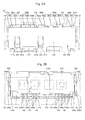
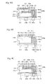
- This shield case 300 as shown in Figs. 1A to 4C , has a receiving portion 310, three folded-back portions 320, a cover 330, a pair of first locking pieces 340a, a pair of second locking pieces 340b, a first back cover 350a, a pair of second back covers 350b, and a pair of third back covers 350c.
- the receiving portion 310 is a cuboid space, shown here in Figs. 1A and 1B as having a generally rectangular tuboid shape.
- the receiving portion 310 has a top plate 311, a bottom plate 312 opposed to the top plate 311, side walls 313 and 314 that connect ends of the top plate 311 and the bottom plate 312.
- the bottom plate 312, as shown in Figs. 1A and 2B is a substantially rectangular plate, the central portion of which is folded into a generally V shape inverted toward the top plate 311.
- the bottom plate 312 is inclined at its left portion shown in Fig. 1A .
- the central portion of the bottom plate 312 protrudes rearward with respect to outer end portions of the bottom plate 312.
- the aforementioned bent portion serves as a partition 312a that sections or divides the inside space of the receiving portion 310 into first and second receiving holes 310a and 310b.
- the first and second receiving holes 310a and 310b have inner shapes conforming to outer shapes of the USB 2.0 plug and the USB 3.0 plug, respectively. That is, the first receiving hole 310a and the second receiving hole 310b are adapted to receive the USB 2.0 plug and the USB 3.0 plug, respectively.
- the top plate 311 is a generally rectangular plate as shown in Figs. 1A and 2A .
- the top plate 311 is provided with a pair of cut-and-raised pieces 311a formed by cutting and raising portions of the top plate 311.
- the rear portion of the top plate 311 is provided with three projections 311b projecting toward the bottom plate 312.
- the side wall 313 is a generally rectangular plate.
- the side wall 314 is a generally rectangular plate of a smaller height dimension than the side wall 313.
- Guide pieces 313a and 314a projecting rearward are provided at rear ends of lower ends of the side walls 313 and 314, respectively, as shown in Figs. 1B , 2A , 2B , 3A and 3B .
- the distance between the guide pieces 313a and 314a is slightly larger than a width dimension of a main body 110 of the body 100.
- the folded-back portions 320 are plate bodies each having a lateral U shape in cross-sectional view, as shown in Figs. 3 and 4 .
- the three folded-back portions 320 extend from the widthwise center and opposite ends of the front end of the top plate 311, and they are folded backward, toward the rear side of the shield case 300.
- the cover 330 is provided continuously to upper ends of the folded-back portions 320.
- the cover 330 is a generally downward U-shaped plate as shown in Figs. 1A and 1B .
- the cover 330 has a central reinforcing plate 331 and a pair of side reinforcing plates 332 (end portions).
- the central reinforcing plate 331 is a generally rectangular plate extending along an upper surface of the top plate 311.
- the central reinforcing plate 331 has a larger width than the top plate 311, the front face of which is continued to the folded-back portions 320.
- the central reinforcing plate 331 has generally rectangular long holes 331a at positions corresponding to the cut-and-raised pieces 311a of the top plate 311.
- the side reinforcing plates 332, as shown in Figs. 1A and 1B are generally rectangular plates provided continuously to opposite end portions of the central reinforcing plate 331 and extending along outer surfaces of the side walls 313, 314.
- the lower end of each of the side reinforcing plates 332 is provided with one of the first locking pieces 340a and one of the second locking pieces 340b extending downward.
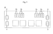
- the first and second locking pieces 340a and 340b are to be inserted into locking holes 11 and 12, respectively, of the circuit board 10 and be connected to ground.
- the first back cover 350a is provided continuously from a central rear end of the top plate 311 of the receiving portion 310, as shown in Fig. 1B .
- the second back covers 350b are provided on either side of the first back cover 350a, also continuously from the rear end of the top plates 311 of the receiving portion 310, as shown in Fig. 1B .
- the third back covers 350c are provided continuously from upper rear ends of the side walls 313 and 314 of the receiving portion 310, as shown in Fig. 1B .
- the first back cover 350a has a bent portion 351a and a cover main portion 352a, which is a generally rectangular plate provided continuously from the bent portion 351a.
- the bent portion 351a is bent substantially at a right angle to the top plate 311, so that the cover main portion 352a extends along and in abutment with a central portion of a rear face of the main body 110 of the body 100.
- Each of the second back covers 350b has a pair of bent portions 351b and a cover main portion 352b, which is a substantially L-shaped plate provided continuously from the bent portions 351b.
- Each of the third back covers 350c has a bent portion 351c and a cover main portion 352c, which is a generally rectangular plate provided continuously from the bent portion 351c.
- the bent portions 351b are bent substantially at a right angle with respect to the top plate 311, and the bent portions 351c are bent substantially at a right angle with respect to the side walls 313 and 314.
- the cover main portions 352b and 352c extend along and in abutment with opposite end portions of the rear face of the main body 110 of the body 100.
- the body 100 is a molded article of insulating resin as shown in Fig. 1A .
- the body 100 has the aforementioned main body 110 and first and second projected portions 120a, 120b.
- the main body 110 is a plate-like body having a generally rectangular shape in cross-sectional view and is housed in the receiving portion 310 of the shield case 300.
- the upper end of the main body 110 is provided with three fitting recesses 111.
- the fitting recesses 111 fittingly receive the projections 311b of the shield case 300, such that bottom surfaces of the fitting recesses 111 abut the projections 311b. As shown in Fig.
- a rear-side lower end of the main body 110 is provided with a pair of outer elongated protrusions 112 and a central elongated protrusion 113 located between the outer elongated protrusions 112. Front surfaces of the outer elongated protrusions 112 abut against outer end portions of the rear end of the bottom plate 312 of the shield case 300, and a front surface of the central elongated protrusion 113 abuts against a central portion of the rear end of the bottom plate 312 of the shield case 300. Moreover, as shown in Figs.
- the rear end surface of the main body 110 abuts the cover main portions 352a, 352b, 352c of the first, second and third back covers 350a, 350b, 350c. That is, the main body 110 is sandwiched between the projections 311b of the shield case 300 and the rear end of the bottom plate 312, and the cover main portions 352a, 352b, 352c of the first, second and third back covers 350a, 350b, 350c. Moreover, the respective outer faces of the outer elongated protrusions 112 of the main body 110 abut the guide pieces 313a, 314b, respectively, as shown in Fig. 2B .
- the first projected portion 120a and the second projected portion 120b extend from front surfaces of the right and left portions, respectively as shown in Fig. 1A , of the body 100.
- the first projected portion 120a is a flat plate-like projection and disposed inside the first receiving hole 310a of the receiving portion 310 of the shield case 300.
- a plurality of long grooves 121a are formed at spaced intervals along the width of a lower face of the first projected portion 120a.
- the second projected portion 120b is a flat plate-like projection and disposed inside the second receiving hole 310b of the receiving portion 310 of the shield case 300.
- a plurality of long grooves 121b are formed at spaced intervals along the width of a lower face of the second projected portion 120b.
- the first contacts 200a are buried by insert molding at spaced intervals (at the same pitch as the long grooves 121a) in the width direction inside the right portion of the main body 110 and the first projected portion 120a.
- the second contacts 200b are buried by insert molding at spaced intervals (at the same pitch as the long grooves 121b) in the width direction inside the left portion of the main body 110 and the second projected portion 120b.
- the first contacts 200a are elongated conductive metal plates of generally L shape as shown in Fig. 4A .
- the first contacts 200a each have a generally L-shaped intermediate portion 210a, a distal end portion 220a continuing to the distal end of the intermediate portion 210a, and a tail portion 230a provided continuously to the rear end of the intermediate portion 210a.
- the intermediate portions 210a are buried in the main body 110 of the body 100, and rear ends thereof protrude downward from one of the outer protrusions 112 of the main body 110.
- the distal end portions 220a are buried in the first projected portion 120a, and lower ends thereof are exposed from the long grooves 121a of the first projected portion 120a.
- the tail portions 230a extend rearward across a lower face of the outer protrusions 112 of the body 100.
- the tail portions 230a are adapted to be connected by soldering to electrodes 13a of the circuit board 10.
- the second contacts 200b are elongated conductive metal plates of generally L shape as shown in Fig. 4C .
- the second contacts 200b each have a generally L-shaped intermediate portion 210b, a distal end portion 220b continuing to the distal end of the intermediate portion 210b, and a tail portion 230b provided continuously to the rear end of the intermediate portion 210b.
- the intermediate portions 210b are buried in the main body 110 of the body 100, and rear ends thereof protrude downward from the other outer protrusion 112 of the main body 110.
- the distal end portions 220b are buried in the second projected portion 120b, and lower ends thereof are exposed from the long grooves 121b of the second projected portion 120b.
- the tail portions 230b extend rearward across the lower face of the outer protrusion 112 of the body 100.
- the tail portions 230b are adapted to be connected by soldering to electrodes 13b of the circuit board 10.
- the receptacle according to the embodiment is configured as described above and assembled as described below.
- the body 100 in which the first and second contacts 200a, 200b are insert-molded is prepared.
- the shield case 300 is also prepared before the bent portions 351a, 351b, 351c of the first, second and third back covers 350a, 350b, 350c are bent.
- the prepared body 100 is inserted through a rear-side opening in the receiving portion 310 of the shield case 300.
- the first and second projected portions 120a, 120b of the body 100 are inserted into the first and second receiving holes 310a, 310b of the receiving portion 310, and the widthwise ends of the main body 110 of the body 100 are brought into abutment with and guided by the pair of guide pieces 313a, 314a of the shield case 300.
- the projections 311b of the shield case 300 are fitted into the fitting recesses 111 of the main body 110 of the body 100, and the outer elongated protrusions 112 of the body 100 abut the outer end portions of the bottom plate 312 of the shield case 300, and the central elongated protrusion 113 of the body 100 abuts the central portion of the bottom plate 312 of the shield case 300.
- bent portions 351a, 351b, 351c of the first, second and third back covers 350a, 350b, 350c are bent substantially at a right angle, so that the cover main portions 352a, 352b, 352c of the first, second and third back covers 350a, 350b, 350c abut the rear end face of the main body 110 of the body 100.
- the receptacle is thus assembled and then mounted on the circuit board 10 in the following manner.
- the first and second locking pieces 340a, 340b of the shield case 300 are inserted into the locking holes 11, 12 of the circuit board 10, and the bottom plate 312 of the shield case 300 is placed on the circuit board 10.
- the tail portions 230a, 230b of the first and second contacts 200a, 200b are placed on the electrodes 13a and 13b, respectively, of the circuit board 10.
- the first and second locking pieces 340a, 340b are connected by soldering with the locking holes 11, 12 of the circuit board 10
- the tail portions 230a, 230b are connected by soldering with the electrodes 13a and 13b, respectively, of the circuit board 10.
- the receptacle assembled as described above can be connected with a USB 2.0 plug and/or a USB 3.0 plug in the following manner.
- a USB 2.0 plug When a USB 2.0 plug is inserted into the first receiving hole 310a of the receiving portion 310 of the shield case 300, the contacts of the USB 2.0 plug come into contact with the distal end portions 220a of the first contacts 200a exposed from the long grooves 121a of the first projected portion 120a of the body 100.
- the USB 2.0 plug is thus connected to the present receptacle.
- USB 3.0 plug When a USB 3.0 plug is inserted into the second receiving hole 310b of the receiving portion 310 of the shield case 300, the contacts of the USB 3.0 plug come into contact with the distal end portions 220b of the second contacts 200b exposed from the long grooves 121b of the second projected portion 120b of the body 100. The USB 3.0 plug is thus connected to the present receptacle.
- the central reinforcing plate of the shield case 300 is disposed along the top plate 311 and the side reinforcing plates 332 are disposed along the side walls 313, 314 of the receiving portion 310. That is, the shield case 300 has a double-layer structure: a first layer consisting of the top plate 311 and the side walls 313, 314 of the receiving portion 310 and a second layer consisting of the central reinforcing plate 331 and the side reinforcing plates 332 of the cover 330.
- the shield case 300 is unlikely to warp, particularly at the top plate 311 of the receiving portion 310, even if a prying or twisting force in the circumferential direction is applied on the receptacle by a USB 2.0 plug inserted into the first receiving hole 310a of the receiving portion 310 of the shield case 300, or by a USB 3.0 plug inserted into the second receiving hole 310b of the receiving portion 310.
- the shield case 300 of the present receptacle has an advantageously high twisting resistance.
- the shield case 300 is easy to fabricate by press molding owing to a single piece structure, essentially consisting of the receiving portion 310, the folded-back portions 320 provided along the front end of the top plate 311 of the receiving portion 310 and folded back rearward, the cover 330 extending from the folded-back portions 320, the pair of first and second locking pieces 340a, 340b extended from the lower ends of the side reinforcing plates 332 of the cover 330, the first back cover 350a and the pair of second back covers 350b, which three back covers extend continuously from the rear end of the top plate 311 of the receiving portion 310, and the pair of third back covers 350c extended continuously from the side walls 313, 314 of the receiving portion 310.
- first and second locking pieces 340a, 340b also extends continuously from the lower ends of the side reinforcing plates 332 of the cover 330. This makes it unnecessary to form locking pieces by cutting out the bottom plate 312 of the receiving portion 310, so that holes will not be formed at such cut-out portions of the bottom plate 312. Consequently, the receiving portion 310 will not allow entry of solder and flux when the receptacle is placed on the circuit board 10 and the first and second locking pieces 340a, 340b are connected by soldering with the locking holes 11, 12 of the circuit board 10.
- the elimination of holes is also advantageous in that a USB 2.0 plug and a USB 3.0 plug inserted into the first and second receiving holes 310a, 310b of the receiving portion 310 will not get stuck with the holes.
- the body 100 can be easily fixed inside the receiving portion 310 of the shield case 300. More particularly, when the body 100 is inserted into the receiving portion 310 of the shield case 300, simply by fitting the projections 311b of the shield case 300 in the recesses 111 of the main body 110, and bringing the outer elongated protrusions 112 and the central elongated protrusion 113 of the main body 110 into abutment with the bottom plate 312 of the shield case 300, and then bending the bent portions 351a, 351b, 351c of the first, second and third back covers 350a, 350b, 350c in such a manner that the cover main portions 352a, 352b, 352c abut the rear end surface of the main body 110, the main body 110 will be sandwiched between the projections 311b and the bottom plate 312 of the shield case 300, and the cover main portions 352a, 352b, 352c.
- the body 100 can be easily incorporated into the receiving portion 310. Further, when the body 100 is inserted into the receiving portion 310 of the shield case 300, the pair of outer elongated protrusions 112 of the main body 110 of the body 100 is guided by the pair of guide pieces 313a, 314a of the shield case 300. Therefore, it is easy to fit the projections 311b of the shield case 300 into the recesses 111 of the main body 110.
- cover main portions 352a, 352b, 352c of the first, second, third back covers 350a, 350b, 350c cover the rear end face of the main body 110.
- the present receptacle is therefore improved in terms of impedance matching and EMI characteristics.
- the shield case 300 of the above embodiment is adapted to receive a USB 2.0 Micro plug connector and a USB 3.0 Micro plug connector into the first and second receiving holes 310a, 310b, respectively, of the receiving portion 310 thereof.
- the present invention is not limited thereto, but the first and second receiving holes 310a, 310b may receive a plug connector of a type other than the Micro USB 2.0 plug connector and the Micro USB 3.0 plug connector.
- the receiving portion 310 of the present invention is not limited to the above embodiment wherein the inside of the receiving portion 310 is sectioned into the first and second receiving holes 310a, 310b with the partition 312a of the bottom plate 312. Instead, the receiving portion 310 may have a single receiving hole without a partition for receiving a plug connector.
- the receiving holes of the receiving portion may receive at least one plug or receptacle connector. That is, the present invention can be applied not only to a receptacle connector but also to a plug connector. If the partition 312a is provided, it can be formed by folding the bottom plate 312 of the receiving portion 310 as in the above embodiment, or by cutting and raising a portion of the bottom plate 312 of the receiving portion 310, or by providing a separate partition on the bottom plate 312.
- the folded-back portions 320 of the above embodiment are provided along the front end of the top plate 311 of the receiving portion 310 and folded back toward the rear side.
- a single folded back portion may be provided at or along the front end of the top plate 311.
- at least one folded-back portion may be provided at or along the rear end of the top plate 311 and folded back toward the front side.
- the folded-back portions 320 may be provided along front or rear ends of the side walls 313, 314.
- the folded-back portions 320 may be of a generally U shape in plan view to connect the front or rear ends of the side walls 313, 314 and the front or rear ends of the side reinforcing plates 332. If the folded-back portions 320 are provided along the rear ends of the top plate 311 or the side walls 313, 314, the first, second and third back covers 350a, 350b, 350c may be omitted.
- the present invention is not limited to the above embodiment where the projections 311b of the top plate 311 of the receiving portion 310 are fitted in the fitting recesses 111 of the main body 110 of the body 100. It is possible to provide a single projection 311b or even possible to omit the projections 311b. Moreover, the projections 311b may be adapted to abut the front face of the main body 110. Similarly, the bottom plate 312 of the receiving portion 310 of the embodiment described in detail above is configured such that its rear end abuts the outer elongated protrusions 112 and the central elongated protrusion 113 of the main body 110.
- the bottom plate 312 of the receiving portion 310 may abut only the outer elongated protrusions 112, or only the central elongated protrusion 113, or none of the elongated protrusions 112 and 113.
- the bottom plate 312 may have the central portion protruding rearward as in the above embodiment, or it may have a central portion flush with the outer end portions.
- the shield case 300 may or may not have the first, second and third back covers 350a, 350b, 350c as in the above embodiment.
- the shield case 300 may have at least one of the first, second and third back covers 350a, 350b, 350c, or may have none of the back covers.
- the first, second and third back covers 350a, 350b, 350c may not be provided along rear end of the receiving portion 310 as in the above embodiment, but they may be provided along the rear end of the cover 330.
- the present invention is not limited to the above embodiment wherein the first and second locking pieces 340a, 340b extend from the lower ends of the side reinforcing plates 332 of the cover 330.
- the first and second locking pieces 340a, 340b may be formed by cutting out portions of the side reinforcing plates 332.
- the first and second locking pieces 340a, 340b may be provided on the bottom plate 312 of the receiving portion 310. At least one of the paired first locking pieces 340a or the paired second locking pieces 340b will suffice.
- the first and second locking pieces 340a, 340b may be omitted if the present connector is applied to a plug connector.
- the shield case 300 of the above embodiment is fabricated by press-molding a metal plate.
- the shield case 300 may be fabricated by depositing metal onto an inner surface of a case made of insulating resin.
- the shape of the body 100 can be changed in accordance with shapes of the connection targets to be inserted into the receiving holes of the receiving portion as needed.
- the shapes and array of the contacts 200a, 200b can be changed in accordance with the shapes of the connection targets as needed.
- the materials, shapes, numbers, dimensions, etc. constituting the receptacle connector of the above embodiment are described as examples only.
- the materials, etc. may be modified as long as they can provide similar functions.
Landscapes
- Details Of Connecting Devices For Male And Female Coupling (AREA)
Applications Claiming Priority (1)
| Application Number | Priority Date | Filing Date | Title |
|---|---|---|---|
| JP2009246385A JP5312288B2 (ja) | 2009-10-27 | 2009-10-27 | シールドケース及びこれを備えたコネクタ |
Publications (2)
| Publication Number | Publication Date |
|---|---|
| EP2320526A1 true EP2320526A1 (de) | 2011-05-11 |
| EP2320526B1 EP2320526B1 (de) | 2016-09-07 |
Family
ID=43437521
Family Applications (1)
| Application Number | Title | Priority Date | Filing Date |
|---|---|---|---|
| EP10251851.1A Not-in-force EP2320526B1 (de) | 2009-10-27 | 2010-10-26 | Abschirmungsgehäuse und Verbinder damit |
Country Status (6)
| Country | Link |
|---|---|
| US (1) | US8182287B2 (de) |
| EP (1) | EP2320526B1 (de) |
| JP (1) | JP5312288B2 (de) |
| KR (1) | KR101691665B1 (de) |
| CN (1) | CN102074836B (de) |
| TW (1) | TWI500220B (de) |
Families Citing this family (13)
| Publication number | Priority date | Publication date | Assignee | Title |
|---|---|---|---|---|
| JP5567882B2 (ja) * | 2010-03-31 | 2014-08-06 | 第一電子工業株式会社 | 電気コネクタ |
| TWI479324B (zh) * | 2012-01-05 | 2015-04-01 | Wistron Corp | 連接介面及傳輸線 |
| CN103456342A (zh) * | 2012-05-30 | 2013-12-18 | 凡甲电子(苏州)有限公司 | 便携式数据存储设备 |
| JP2014082102A (ja) * | 2012-10-16 | 2014-05-08 | Smk Corp | レセプタクルコネクタ |
| KR102148054B1 (ko) * | 2013-04-26 | 2020-08-25 | 소니 주식회사 | 커넥터, 데이터 송신 장치, 데이터 수신 장치 및 데이터 송수신 시스템 |
| JP6063808B2 (ja) * | 2013-04-26 | 2017-01-18 | 日本航空電子工業株式会社 | 電気コネクタ |
| US9197020B2 (en) * | 2013-09-06 | 2015-11-24 | Sonetek Technology Corp. | Mini USB connector |
| TWM480790U (zh) * | 2013-12-13 | 2014-06-21 | Advanced Connectek Inc | 具有肋結構的插座電連接器 |
| JP5968945B2 (ja) * | 2014-04-08 | 2016-08-10 | レノボ・シンガポール・プライベート・リミテッド | 雌コネクタ |
| WO2015164538A1 (en) | 2014-04-23 | 2015-10-29 | Tyco Electronics Corporation | Electrical connector with shield cap and shielded terminals |
| CN204946606U (zh) * | 2015-07-22 | 2016-01-06 | 富士康(昆山)电脑接插件有限公司 | 线缆 |
| USD896180S1 (en) * | 2018-07-03 | 2020-09-15 | Asustek Computer Inc. | Connector |
| JP7307006B2 (ja) * | 2020-02-14 | 2023-07-11 | ヒロセ電機株式会社 | シールド電気コネクタ |
Citations (4)
| Publication number | Priority date | Publication date | Assignee | Title |
|---|---|---|---|---|
| JPH03109294A (ja) | 1989-09-22 | 1991-05-09 | New Japan Radio Co Ltd | ダイヤモンドコーティング装置 |
| US5800204A (en) * | 1995-11-09 | 1998-09-01 | Molex Incorporated | Electrical connector for flat cable |
| US6416359B1 (en) * | 2001-04-27 | 2002-07-09 | Hon Hai Precision Ind. Co., Ltd. | Electrical connector |
| EP1274155A1 (de) * | 2001-07-04 | 2003-01-08 | Japan Aviation Electronics Industry, Limited | Verbinder für Kupplung mit verschiedenen Verbindern die verschiedene Anpassungsformen ausweisen |
Family Cites Families (17)
| Publication number | Priority date | Publication date | Assignee | Title |
|---|---|---|---|---|
| US5044980A (en) * | 1990-01-16 | 1991-09-03 | Beta Phase, Inc. | High density and multiple insertion connector |
| JP3109294B2 (ja) | 1992-10-22 | 2000-11-13 | 富士ゼロックス株式会社 | 給紙トレイ |
| JPH0945404A (ja) * | 1995-07-28 | 1997-02-14 | Yazaki Corp | 雌端子 |
| JP3196018B2 (ja) * | 1997-03-31 | 2001-08-06 | 日本航空電子工業株式会社 | シールド機構付き中継コネクタ |
| US6036520A (en) * | 1997-12-12 | 2000-03-14 | Molex Incorporated | Electrical connector for flat circuitry |
| US6027363A (en) * | 1998-04-22 | 2000-02-22 | Molex Incorporated | Electrical connector for flat flexible circuitry |
| CN2417599Y (zh) * | 2000-02-10 | 2001-01-31 | 莫列斯公司 | 具有防短路结构的连接器 |
| JP2002252048A (ja) * | 2001-02-23 | 2002-09-06 | Auto Network Gijutsu Kenkyusho:Kk | コネクタ端子及び同コネクタ端子の製造方法 |
| TW553545U (en) * | 2001-09-25 | 2003-09-11 | Molex Inc | High speed transmission connector |
| JP2005141930A (ja) * | 2003-11-04 | 2005-06-02 | Molex Inc | ケーブルコネクタ |
| WO2007000814A1 (ja) * | 2005-06-29 | 2007-01-04 | Fujitsu Limited | コネクタ、回路基板及び電子機器 |
| JP4368897B2 (ja) * | 2007-03-28 | 2009-11-18 | ヒロセ電機株式会社 | コネクタ |
| TWM349070U (en) * | 2008-06-03 | 2009-01-11 | Hon Hai Prec Ind Co Ltd | Electrical connector |
| US7871297B2 (en) * | 2008-06-11 | 2011-01-18 | Lotes Co., Ltd. | Electrical connector assembly |
| TWM345381U (en) * | 2008-06-30 | 2008-11-21 | Niketech Electronic Corp | Structure of the electrical connector |
| US7748997B2 (en) * | 2008-07-22 | 2010-07-06 | Tyco Electronics Corporation | Receptacle for electrical connectors |
| TWM361742U (en) * | 2008-12-09 | 2009-07-21 | Hon Hai Prec Ind Co Ltd | Electrical connector |
-
2009
- 2009-10-27 JP JP2009246385A patent/JP5312288B2/ja active Active
-
2010
- 2010-08-13 TW TW099127121A patent/TWI500220B/zh not_active IP Right Cessation
- 2010-09-17 KR KR1020100091415A patent/KR101691665B1/ko not_active Expired - Fee Related
- 2010-10-01 US US12/896,248 patent/US8182287B2/en not_active Expired - Fee Related
- 2010-10-25 CN CN201010521804.8A patent/CN102074836B/zh not_active Expired - Fee Related
- 2010-10-26 EP EP10251851.1A patent/EP2320526B1/de not_active Not-in-force
Patent Citations (5)
| Publication number | Priority date | Publication date | Assignee | Title |
|---|---|---|---|---|
| JPH03109294A (ja) | 1989-09-22 | 1991-05-09 | New Japan Radio Co Ltd | ダイヤモンドコーティング装置 |
| US5800204A (en) * | 1995-11-09 | 1998-09-01 | Molex Incorporated | Electrical connector for flat cable |
| US6416359B1 (en) * | 2001-04-27 | 2002-07-09 | Hon Hai Precision Ind. Co., Ltd. | Electrical connector |
| EP1274155A1 (de) * | 2001-07-04 | 2003-01-08 | Japan Aviation Electronics Industry, Limited | Verbinder für Kupplung mit verschiedenen Verbindern die verschiedene Anpassungsformen ausweisen |
| JP2003017165A (ja) | 2001-07-04 | 2003-01-17 | Japan Aviation Electronics Industry Ltd | コネクタ |
Also Published As
| Publication number | Publication date |
|---|---|
| US20110097931A1 (en) | 2011-04-28 |
| TWI500220B (zh) | 2015-09-11 |
| CN102074836A (zh) | 2011-05-25 |
| JP2011096381A (ja) | 2011-05-12 |
| KR20110051135A (ko) | 2011-05-17 |
| EP2320526B1 (de) | 2016-09-07 |
| TW201131911A (en) | 2011-09-16 |
| KR101691665B1 (ko) | 2016-12-30 |
| CN102074836B (zh) | 2014-11-26 |
| JP5312288B2 (ja) | 2013-10-09 |
| US8182287B2 (en) | 2012-05-22 |
Similar Documents
| Publication | Publication Date | Title |
|---|---|---|
| EP2320526B1 (de) | Abschirmungsgehäuse und Verbinder damit | |
| US10236638B2 (en) | Electrical connector having separate grounding pieces | |
| US8858237B2 (en) | Receptacle connector having improved contact modules | |
| EP2282375B1 (de) | Verbinder und elektronisches Gerät | |
| US9178319B2 (en) | Electrical connector with shieldingthereof | |
| US6241556B1 (en) | Retention member for connector | |
| US8961235B2 (en) | Electrical connector with improved mating member having anti-mismating portion for preventing incorrect insertion | |
| US6305978B1 (en) | Low profile mini coaxial cable connector | |
| US9525223B2 (en) | Flippable electrical connector | |
| US9812827B2 (en) | Connector having tongue portion with peripheral support unitarily formed with metallic shell | |
| US8202122B2 (en) | Cable connector assembly with improved conductive shell | |
| EP2339702B1 (de) | Steckverbinder | |
| EP2369687B1 (de) | Stecker und elektronisches Gerät | |
| EP2282378B1 (de) | Abschirmungsgehäuse, Büchsenteil und elektronisches Gerät | |
| US11245216B2 (en) | Electrical connector upper and lower contacts made from a single contact carrier and including two outermost contacts with integral latching portions | |
| US6749463B1 (en) | Shielded board mounted electrical connector | |
| US8821195B2 (en) | Connector | |
| EP2369692B1 (de) | Abschirmungsgehäuse, Steckverbinder und elektronisches Gerät | |
| US20060228946A1 (en) | Electrical connector assembly with multi-function latching member | |
| US20160380388A1 (en) | Electrical connector having inserted insulator and method of making the same | |
| US9419385B2 (en) | Cable connector assembly with improved shell | |
| US10333253B2 (en) | Electrical connector with reinforced and thickened metallic shielding plate on front edge of mating tongue | |
| EP2434589B1 (de) | Abschirmungsgehäuse, Steckverbinder mit dem Abschirmungsgehäuse und elektronisches Gerät mit dem Steckverbinder | |
| CN111048953A (zh) | 转角插头连接器及其制造方法 | |
| US20120329322A1 (en) | Connector and signal line structure |
Legal Events
| Date | Code | Title | Description |
|---|---|---|---|
| PUAI | Public reference made under article 153(3) epc to a published international application that has entered the european phase |
Free format text: ORIGINAL CODE: 0009012 |
|
| AK | Designated contracting states |
Kind code of ref document: A1 Designated state(s): AL AT BE BG CH CY CZ DE DK EE ES FI FR GB GR HR HU IE IS IT LI LT LU LV MC MK MT NL NO PL PT RO RS SE SI SK SM TR |
|
| AX | Request for extension of the european patent |
Extension state: BA ME |
|
| 17P | Request for examination filed |
Effective date: 20111014 |
|
| 17Q | First examination report despatched |
Effective date: 20150420 |
|
| REG | Reference to a national code |
Ref country code: DE Ref legal event code: R079 Ref document number: 602010036162 Country of ref document: DE Free format text: PREVIOUS MAIN CLASS: H01R0027020000 Ipc: H01R0012720000 |
|
| GRAP | Despatch of communication of intention to grant a patent |
Free format text: ORIGINAL CODE: EPIDOSNIGR1 |
|
| RIC1 | Information provided on ipc code assigned before grant |
Ipc: H01R 13/6461 20110101ALI20160304BHEP Ipc: H01R 12/72 20110101AFI20160304BHEP Ipc: H01R 27/02 20060101ALI20160304BHEP Ipc: H01R 13/6473 20110101ALI20160304BHEP Ipc: H01R 12/50 20110101ALI20160304BHEP |
|
| INTG | Intention to grant announced |
Effective date: 20160404 |
|
| GRAS | Grant fee paid |
Free format text: ORIGINAL CODE: EPIDOSNIGR3 |
|
| GRAA | (expected) grant |
Free format text: ORIGINAL CODE: 0009210 |
|
| AK | Designated contracting states |
Kind code of ref document: B1 Designated state(s): AL AT BE BG CH CY CZ DE DK EE ES FI FR GB GR HR HU IE IS IT LI LT LU LV MC MK MT NL NO PL PT RO RS SE SI SK SM TR |
|
| REG | Reference to a national code |
Ref country code: GB Ref legal event code: FG4D |
|
| REG | Reference to a national code |
Ref country code: CH Ref legal event code: EP |
|
| REG | Reference to a national code |
Ref country code: IE Ref legal event code: FG4D |
|
| REG | Reference to a national code |
Ref country code: DE Ref legal event code: R096 Ref document number: 602010036162 Country of ref document: DE |
|
| REG | Reference to a national code |
Ref country code: AT Ref legal event code: REF Ref document number: 827594 Country of ref document: AT Kind code of ref document: T Effective date: 20161015 |
|
| REG | Reference to a national code |
Ref country code: FR Ref legal event code: PLFP Year of fee payment: 7 |
|
| REG | Reference to a national code |
Ref country code: LT Ref legal event code: MG4D |
|
| REG | Reference to a national code |
Ref country code: NL Ref legal event code: MP Effective date: 20160907 |
|
| PG25 | Lapsed in a contracting state [announced via postgrant information from national office to epo] |
Ref country code: HR Free format text: LAPSE BECAUSE OF FAILURE TO SUBMIT A TRANSLATION OF THE DESCRIPTION OR TO PAY THE FEE WITHIN THE PRESCRIBED TIME-LIMIT Effective date: 20160907 Ref country code: LT Free format text: LAPSE BECAUSE OF FAILURE TO SUBMIT A TRANSLATION OF THE DESCRIPTION OR TO PAY THE FEE WITHIN THE PRESCRIBED TIME-LIMIT Effective date: 20160907 Ref country code: RS Free format text: LAPSE BECAUSE OF FAILURE TO SUBMIT A TRANSLATION OF THE DESCRIPTION OR TO PAY THE FEE WITHIN THE PRESCRIBED TIME-LIMIT Effective date: 20160907 Ref country code: FI Free format text: LAPSE BECAUSE OF FAILURE TO SUBMIT A TRANSLATION OF THE DESCRIPTION OR TO PAY THE FEE WITHIN THE PRESCRIBED TIME-LIMIT Effective date: 20160907 Ref country code: NO Free format text: LAPSE BECAUSE OF FAILURE TO SUBMIT A TRANSLATION OF THE DESCRIPTION OR TO PAY THE FEE WITHIN THE PRESCRIBED TIME-LIMIT Effective date: 20161207 |
|
| REG | Reference to a national code |
Ref country code: AT Ref legal event code: MK05 Ref document number: 827594 Country of ref document: AT Kind code of ref document: T Effective date: 20160907 |
|
| PG25 | Lapsed in a contracting state [announced via postgrant information from national office to epo] |
Ref country code: NL Free format text: LAPSE BECAUSE OF FAILURE TO SUBMIT A TRANSLATION OF THE DESCRIPTION OR TO PAY THE FEE WITHIN THE PRESCRIBED TIME-LIMIT Effective date: 20160907 Ref country code: LV Free format text: LAPSE BECAUSE OF FAILURE TO SUBMIT A TRANSLATION OF THE DESCRIPTION OR TO PAY THE FEE WITHIN THE PRESCRIBED TIME-LIMIT Effective date: 20160907 Ref country code: GR Free format text: LAPSE BECAUSE OF FAILURE TO SUBMIT A TRANSLATION OF THE DESCRIPTION OR TO PAY THE FEE WITHIN THE PRESCRIBED TIME-LIMIT Effective date: 20161208 Ref country code: SE Free format text: LAPSE BECAUSE OF FAILURE TO SUBMIT A TRANSLATION OF THE DESCRIPTION OR TO PAY THE FEE WITHIN THE PRESCRIBED TIME-LIMIT Effective date: 20160907 Ref country code: BE Free format text: LAPSE BECAUSE OF NON-PAYMENT OF DUE FEES Effective date: 20161031 Ref country code: ES Free format text: LAPSE BECAUSE OF FAILURE TO SUBMIT A TRANSLATION OF THE DESCRIPTION OR TO PAY THE FEE WITHIN THE PRESCRIBED TIME-LIMIT Effective date: 20160907 |
|
| PG25 | Lapsed in a contracting state [announced via postgrant information from national office to epo] |
Ref country code: RO Free format text: LAPSE BECAUSE OF FAILURE TO SUBMIT A TRANSLATION OF THE DESCRIPTION OR TO PAY THE FEE WITHIN THE PRESCRIBED TIME-LIMIT Effective date: 20160907 Ref country code: EE Free format text: LAPSE BECAUSE OF FAILURE TO SUBMIT A TRANSLATION OF THE DESCRIPTION OR TO PAY THE FEE WITHIN THE PRESCRIBED TIME-LIMIT Effective date: 20160907 |
|
| PG25 | Lapsed in a contracting state [announced via postgrant information from national office to epo] |
Ref country code: SK Free format text: LAPSE BECAUSE OF FAILURE TO SUBMIT A TRANSLATION OF THE DESCRIPTION OR TO PAY THE FEE WITHIN THE PRESCRIBED TIME-LIMIT Effective date: 20160907 Ref country code: IS Free format text: LAPSE BECAUSE OF FAILURE TO SUBMIT A TRANSLATION OF THE DESCRIPTION OR TO PAY THE FEE WITHIN THE PRESCRIBED TIME-LIMIT Effective date: 20170107 Ref country code: PT Free format text: LAPSE BECAUSE OF FAILURE TO SUBMIT A TRANSLATION OF THE DESCRIPTION OR TO PAY THE FEE WITHIN THE PRESCRIBED TIME-LIMIT Effective date: 20170109 Ref country code: PL Free format text: LAPSE BECAUSE OF FAILURE TO SUBMIT A TRANSLATION OF THE DESCRIPTION OR TO PAY THE FEE WITHIN THE PRESCRIBED TIME-LIMIT Effective date: 20160907 Ref country code: BE Free format text: LAPSE BECAUSE OF FAILURE TO SUBMIT A TRANSLATION OF THE DESCRIPTION OR TO PAY THE FEE WITHIN THE PRESCRIBED TIME-LIMIT Effective date: 20160907 Ref country code: BG Free format text: LAPSE BECAUSE OF FAILURE TO SUBMIT A TRANSLATION OF THE DESCRIPTION OR TO PAY THE FEE WITHIN THE PRESCRIBED TIME-LIMIT Effective date: 20161207 Ref country code: SM Free format text: LAPSE BECAUSE OF FAILURE TO SUBMIT A TRANSLATION OF THE DESCRIPTION OR TO PAY THE FEE WITHIN THE PRESCRIBED TIME-LIMIT Effective date: 20160907 Ref country code: CZ Free format text: LAPSE BECAUSE OF FAILURE TO SUBMIT A TRANSLATION OF THE DESCRIPTION OR TO PAY THE FEE WITHIN THE PRESCRIBED TIME-LIMIT Effective date: 20160907 Ref country code: AT Free format text: LAPSE BECAUSE OF FAILURE TO SUBMIT A TRANSLATION OF THE DESCRIPTION OR TO PAY THE FEE WITHIN THE PRESCRIBED TIME-LIMIT Effective date: 20160907 |
|
| REG | Reference to a national code |
Ref country code: CH Ref legal event code: PL |
|
| REG | Reference to a national code |
Ref country code: DE Ref legal event code: R097 Ref document number: 602010036162 Country of ref document: DE |
|
| PG25 | Lapsed in a contracting state [announced via postgrant information from national office to epo] |
Ref country code: IT Free format text: LAPSE BECAUSE OF FAILURE TO SUBMIT A TRANSLATION OF THE DESCRIPTION OR TO PAY THE FEE WITHIN THE PRESCRIBED TIME-LIMIT Effective date: 20160907 |
|
| PLBE | No opposition filed within time limit |
Free format text: ORIGINAL CODE: 0009261 |
|
| STAA | Information on the status of an ep patent application or granted ep patent |
Free format text: STATUS: NO OPPOSITION FILED WITHIN TIME LIMIT |
|
| REG | Reference to a national code |
Ref country code: IE Ref legal event code: MM4A |
|
| PG25 | Lapsed in a contracting state [announced via postgrant information from national office to epo] |
Ref country code: LI Free format text: LAPSE BECAUSE OF NON-PAYMENT OF DUE FEES Effective date: 20161031 Ref country code: CH Free format text: LAPSE BECAUSE OF NON-PAYMENT OF DUE FEES Effective date: 20161031 Ref country code: DK Free format text: LAPSE BECAUSE OF FAILURE TO SUBMIT A TRANSLATION OF THE DESCRIPTION OR TO PAY THE FEE WITHIN THE PRESCRIBED TIME-LIMIT Effective date: 20160907 |
|
| 26N | No opposition filed |
Effective date: 20170608 |
|
| PG25 | Lapsed in a contracting state [announced via postgrant information from national office to epo] |
Ref country code: LU Free format text: LAPSE BECAUSE OF NON-PAYMENT OF DUE FEES Effective date: 20161026 Ref country code: SI Free format text: LAPSE BECAUSE OF FAILURE TO SUBMIT A TRANSLATION OF THE DESCRIPTION OR TO PAY THE FEE WITHIN THE PRESCRIBED TIME-LIMIT Effective date: 20160907 |
|
| REG | Reference to a national code |
Ref country code: FR Ref legal event code: PLFP Year of fee payment: 8 |
|
| PG25 | Lapsed in a contracting state [announced via postgrant information from national office to epo] |
Ref country code: IE Free format text: LAPSE BECAUSE OF NON-PAYMENT OF DUE FEES Effective date: 20161026 |
|
| PG25 | Lapsed in a contracting state [announced via postgrant information from national office to epo] |
Ref country code: HU Free format text: LAPSE BECAUSE OF FAILURE TO SUBMIT A TRANSLATION OF THE DESCRIPTION OR TO PAY THE FEE WITHIN THE PRESCRIBED TIME-LIMIT; INVALID AB INITIO Effective date: 20101026 Ref country code: CY Free format text: LAPSE BECAUSE OF FAILURE TO SUBMIT A TRANSLATION OF THE DESCRIPTION OR TO PAY THE FEE WITHIN THE PRESCRIBED TIME-LIMIT Effective date: 20160907 |
|
| PG25 | Lapsed in a contracting state [announced via postgrant information from national office to epo] |
Ref country code: MC Free format text: LAPSE BECAUSE OF FAILURE TO SUBMIT A TRANSLATION OF THE DESCRIPTION OR TO PAY THE FEE WITHIN THE PRESCRIBED TIME-LIMIT Effective date: 20160907 Ref country code: MK Free format text: LAPSE BECAUSE OF FAILURE TO SUBMIT A TRANSLATION OF THE DESCRIPTION OR TO PAY THE FEE WITHIN THE PRESCRIBED TIME-LIMIT Effective date: 20160907 Ref country code: TR Free format text: LAPSE BECAUSE OF FAILURE TO SUBMIT A TRANSLATION OF THE DESCRIPTION OR TO PAY THE FEE WITHIN THE PRESCRIBED TIME-LIMIT Effective date: 20160907 Ref country code: MT Free format text: LAPSE BECAUSE OF NON-PAYMENT OF DUE FEES Effective date: 20161031 |
|
| REG | Reference to a national code |
Ref country code: FR Ref legal event code: PLFP Year of fee payment: 9 |
|
| PG25 | Lapsed in a contracting state [announced via postgrant information from national office to epo] |
Ref country code: AL Free format text: LAPSE BECAUSE OF FAILURE TO SUBMIT A TRANSLATION OF THE DESCRIPTION OR TO PAY THE FEE WITHIN THE PRESCRIBED TIME-LIMIT Effective date: 20160907 |
|
| PGFP | Annual fee paid to national office [announced via postgrant information from national office to epo] |
Ref country code: GB Payment date: 20220901 Year of fee payment: 13 |
|
| PGFP | Annual fee paid to national office [announced via postgrant information from national office to epo] |
Ref country code: FR Payment date: 20220908 Year of fee payment: 13 |
|
| PGFP | Annual fee paid to national office [announced via postgrant information from national office to epo] |
Ref country code: DE Payment date: 20220831 Year of fee payment: 13 |
|
| REG | Reference to a national code |
Ref country code: DE Ref legal event code: R119 Ref document number: 602010036162 Country of ref document: DE |
|
| GBPC | Gb: european patent ceased through non-payment of renewal fee |
Effective date: 20231026 |
|
| PG25 | Lapsed in a contracting state [announced via postgrant information from national office to epo] |
Ref country code: GB Free format text: LAPSE BECAUSE OF NON-PAYMENT OF DUE FEES Effective date: 20231026 |
|
| PG25 | Lapsed in a contracting state [announced via postgrant information from national office to epo] |
Ref country code: GB Free format text: LAPSE BECAUSE OF NON-PAYMENT OF DUE FEES Effective date: 20231026 Ref country code: FR Free format text: LAPSE BECAUSE OF NON-PAYMENT OF DUE FEES Effective date: 20231031 Ref country code: DE Free format text: LAPSE BECAUSE OF NON-PAYMENT OF DUE FEES Effective date: 20240501 |