EP2325736B1 - Écran tactile et son procédé de commande - Google Patents
Écran tactile et son procédé de commande Download PDFInfo
- Publication number
- EP2325736B1 EP2325736B1 EP10251292.8A EP10251292A EP2325736B1 EP 2325736 B1 EP2325736 B1 EP 2325736B1 EP 10251292 A EP10251292 A EP 10251292A EP 2325736 B1 EP2325736 B1 EP 2325736B1
- Authority
- EP
- European Patent Office
- Prior art keywords
- sensing
- driving
- electric field
- active stylus
- signal
- Prior art date
- Legal status (The legal status is an assumption and is not a legal conclusion. Google has not performed a legal analysis and makes no representation as to the accuracy of the status listed.)
- Active
Links
Images




Classifications
-
- G—PHYSICS
- G06—COMPUTING OR CALCULATING; COUNTING
- G06F—ELECTRIC DIGITAL DATA PROCESSING
- G06F3/00—Input arrangements for transferring data to be processed into a form capable of being handled by the computer; Output arrangements for transferring data from processing unit to output unit, e.g. interface arrangements
- G06F3/01—Input arrangements or combined input and output arrangements for interaction between user and computer
- G06F3/03—Arrangements for converting the position or the displacement of a member into a coded form
- G06F3/041—Digitisers, e.g. for touch screens or touch pads, characterised by the transducing means
- G06F3/044—Digitisers, e.g. for touch screens or touch pads, characterised by the transducing means by capacitive means
-
- G—PHYSICS
- G06—COMPUTING OR CALCULATING; COUNTING
- G06F—ELECTRIC DIGITAL DATA PROCESSING
- G06F3/00—Input arrangements for transferring data to be processed into a form capable of being handled by the computer; Output arrangements for transferring data from processing unit to output unit, e.g. interface arrangements
- G06F3/01—Input arrangements or combined input and output arrangements for interaction between user and computer
- G06F3/03—Arrangements for converting the position or the displacement of a member into a coded form
- G06F3/033—Pointing devices displaced or positioned by the user, e.g. mice, trackballs, pens or joysticks; Accessories therefor
- G06F3/0354—Pointing devices displaced or positioned by the user, e.g. mice, trackballs, pens or joysticks; Accessories therefor with detection of two-dimensional [2D] relative movements between the device, or an operating part thereof, and a plane or surface, e.g. 2D mice, trackballs, pens or pucks
- G06F3/03545—Pens or stylus
-
- G—PHYSICS
- G06—COMPUTING OR CALCULATING; COUNTING
- G06F—ELECTRIC DIGITAL DATA PROCESSING
- G06F3/00—Input arrangements for transferring data to be processed into a form capable of being handled by the computer; Output arrangements for transferring data from processing unit to output unit, e.g. interface arrangements
- G06F3/01—Input arrangements or combined input and output arrangements for interaction between user and computer
- G06F3/03—Arrangements for converting the position or the displacement of a member into a coded form
- G06F3/033—Pointing devices displaced or positioned by the user, e.g. mice, trackballs, pens or joysticks; Accessories therefor
- G06F3/0354—Pointing devices displaced or positioned by the user, e.g. mice, trackballs, pens or joysticks; Accessories therefor with detection of two-dimensional [2D] relative movements between the device, or an operating part thereof, and a plane or surface, e.g. 2D mice, trackballs, pens or pucks
-
- G—PHYSICS
- G06—COMPUTING OR CALCULATING; COUNTING
- G06F—ELECTRIC DIGITAL DATA PROCESSING
- G06F3/00—Input arrangements for transferring data to be processed into a form capable of being handled by the computer; Output arrangements for transferring data from processing unit to output unit, e.g. interface arrangements
- G06F3/01—Input arrangements or combined input and output arrangements for interaction between user and computer
- G06F3/03—Arrangements for converting the position or the displacement of a member into a coded form
- G06F3/041—Digitisers, e.g. for touch screens or touch pads, characterised by the transducing means
- G06F3/0412—Digitisers structurally integrated in a display
-
- G—PHYSICS
- G06—COMPUTING OR CALCULATING; COUNTING
- G06F—ELECTRIC DIGITAL DATA PROCESSING
- G06F3/00—Input arrangements for transferring data to be processed into a form capable of being handled by the computer; Output arrangements for transferring data from processing unit to output unit, e.g. interface arrangements
- G06F3/01—Input arrangements or combined input and output arrangements for interaction between user and computer
- G06F3/03—Arrangements for converting the position or the displacement of a member into a coded form
- G06F3/041—Digitisers, e.g. for touch screens or touch pads, characterised by the transducing means
- G06F3/0416—Control or interface arrangements specially adapted for digitisers
- G06F3/04166—Details of scanning methods, e.g. sampling time, grouping of sub areas or time sharing with display driving
-
- G—PHYSICS
- G06—COMPUTING OR CALCULATING; COUNTING
- G06F—ELECTRIC DIGITAL DATA PROCESSING
- G06F3/00—Input arrangements for transferring data to be processed into a form capable of being handled by the computer; Output arrangements for transferring data from processing unit to output unit, e.g. interface arrangements
- G06F3/01—Input arrangements or combined input and output arrangements for interaction between user and computer
- G06F3/03—Arrangements for converting the position or the displacement of a member into a coded form
- G06F3/041—Digitisers, e.g. for touch screens or touch pads, characterised by the transducing means
- G06F3/044—Digitisers, e.g. for touch screens or touch pads, characterised by the transducing means by capacitive means
- G06F3/0442—Digitisers, e.g. for touch screens or touch pads, characterised by the transducing means by capacitive means using active external devices, e.g. active pens, for transmitting changes in electrical potential to be received by the digitiser
-
- G—PHYSICS
- G06—COMPUTING OR CALCULATING; COUNTING
- G06F—ELECTRIC DIGITAL DATA PROCESSING
- G06F3/00—Input arrangements for transferring data to be processed into a form capable of being handled by the computer; Output arrangements for transferring data from processing unit to output unit, e.g. interface arrangements
- G06F3/01—Input arrangements or combined input and output arrangements for interaction between user and computer
- G06F3/03—Arrangements for converting the position or the displacement of a member into a coded form
- G06F3/041—Digitisers, e.g. for touch screens or touch pads, characterised by the transducing means
- G06F3/044—Digitisers, e.g. for touch screens or touch pads, characterised by the transducing means by capacitive means
- G06F3/0445—Digitisers, e.g. for touch screens or touch pads, characterised by the transducing means by capacitive means using two or more layers of sensing electrodes, e.g. using two layers of electrodes separated by a dielectric layer
-
- G—PHYSICS
- G06—COMPUTING OR CALCULATING; COUNTING
- G06F—ELECTRIC DIGITAL DATA PROCESSING
- G06F3/00—Input arrangements for transferring data to be processed into a form capable of being handled by the computer; Output arrangements for transferring data from processing unit to output unit, e.g. interface arrangements
- G06F3/01—Input arrangements or combined input and output arrangements for interaction between user and computer
- G06F3/03—Arrangements for converting the position or the displacement of a member into a coded form
- G06F3/041—Digitisers, e.g. for touch screens or touch pads, characterised by the transducing means
- G06F3/044—Digitisers, e.g. for touch screens or touch pads, characterised by the transducing means by capacitive means
- G06F3/0446—Digitisers, e.g. for touch screens or touch pads, characterised by the transducing means by capacitive means using a grid-like structure of electrodes in at least two directions, e.g. using row and column electrodes
-
- G—PHYSICS
- G06—COMPUTING OR CALCULATING; COUNTING
- G06F—ELECTRIC DIGITAL DATA PROCESSING
- G06F2203/00—Indexing scheme relating to G06F3/00 - G06F3/048
- G06F2203/041—Indexing scheme relating to G06F3/041 - G06F3/045
- G06F2203/04104—Multi-touch detection in digitiser, i.e. details about the simultaneous detection of a plurality of touching locations, e.g. multiple fingers or pen and finger
Definitions
- the present invention relates to a touch screen system and a method of driving the same.
- a touch screen panel is an input device capable of detecting a user's indication or selection of content displayed on an image display device using a finger or an object.
- the touch screen panel is provided on the front face of the image display device to convert a contact position between the touch screen panel and the finger or the object into an electrical signal. Therefore, the contact position is received as an input signal. Since the touch screen panel may replace or complement another input device coupled to the image display device such as a keyboard and a mouse, the variety of uses of touch screen panels is increasing.
- US 5,369,227 discloses an active stylus for a capacitance tablet emitting an electric field at different frequencies.
- US 7,612,767 discloses a pen or stylus for use with a self-capacitive touch pad, which aims to simulate the effect of touch by a finger by coupling negative voltage transitions to the nearby touch pad electrodes and aligning these negative voltage transitions such that they occur just before the rising edges of the touch pad's internal AC voltage signal.
- US 5,790,106 discloses a capacitance touch screen which can detect a touch by a finger or an active stylus, wherein the stylus can be distinguished from a finger by the voltage level on the sensing lines.
- embodiments of the present invention are directed to a touch screen system using a mutual capacitance method that is capable of implementing both multi-touch recognition by an active stylus and multi-touch recognition by a finger and a method of driving the same.
- the present invention provides a touch screen system according to claim 1.
- the signal generated by the signal generator may be an AC voltage having a same phase as the driving signal.
- the electric field emitter may include a non-inverting amplifier for maintaining a phase of the signal generated by the signal generator to amplify the signal and to output the active stylus electric field.
- the electric field emitter may include an inverting amplifier for inverting a phase of the signal generated by the signal generator to output the active stylus electric field.
- the active stylus may further include a frequency converter for converting the frequency of the AC voltage generated by the signal generator.
- the sensing circuit may include a level detector for detecting levels of the first sensing signals and an ADC for converting the first sensing signals into the second sensing signals to provide second sensing signals to the processor.
- the touch screen system may further include a frequency filter for filtering signals having a specific frequency among the first sensing signals.
- the frequency filter may include a bandpass filter.
- the plurality of driving lines and the plurality of sensing lines may be located on different layers on a transparent substrate with an insulating layer interposed therebetween and comprise a transparent conductive material.
- the mutual capacitances may be formed in the sensing cells at crossing regions between the driving lines and the sensing lines.
- the sensing cells may be configured to supply the first sensing signals corresponding to their mutual capacitances to the sensing lines they are coupled to when driving signals are applied from the driving circuit to the driving lines coupled to the sensing cells.
- Another aspect of the present invention is directed toward a method of driving a touch screen system according to claim 12.
- the method may further include distinguishing a change in the mutual capacitance generated when the finger contacts the at least one sensing cell from a change in the mutual capacitance generated when the active stylus contacts the at least one sensing cell when determining the position of the sensing cell.
- the AC voltage may have a same phase as the driving signal.
- the amplified AC voltage may have its phase inverted to be output.
- the method further may further include converting the frequency of the AC voltage.
- multi-touch recognition of a finger and multi-touch recognition of an active stylus may be concurrently implemented using a touch screen panel in a mutual capacitance method and the multi-touch recognition of the finger is distinguished from the multi-touch recognition of the active stylus to recognize various and precise multi-touch situations.
- first element when a first element is described as being coupled to a second element, the first element may be directly coupled to the second element or may be indirectly coupled to the second element via a third element. Further, some of the elements that are not essential to a complete understanding of the invention are omitted for clarity. Also, like reference numerals refer to like elements throughout.
- touch recognition may be implemented through a self capacitance method and/or a mutual capacitance method.
- a human body part e.g., a finger
- a contact surface of the input panel is detected due to a change in the electrostatic capacitance formed in a sensing cell (node) positioned on the contact surface when it is placed near the electric field of a human body.
- a stylus or other pointing device may be used.
- a passive stylus can typically only cause a small change in the electrostatic capacitance on the contact surface so that it is difficult to detect its position.
- an active stylus which generates its own an electric field, may affect not only the sensing cell (node) of the touch screen panel corresponding to the position that the stylus is actually in contact with, but also the other neighboring sensing cells (nodes) so that it is also difficult to determine the contact position of an active stylus.
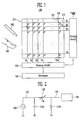
- FIG. 1 is a block diagram illustrating a touch screen system according to one embodiment of the present invention.
- FIG. 2 is a simplified circuit diagram illustrating the touch screen panel of FIG. 1 .
- a touch screen system 100 includes a plurality of driving lines 112 (e.g., X1, X2, ..., Xn) arranged in a first direction, a plurality of sensing lines 114 (e.g., Y1, Y2, ..., Ym) arranged in a direction that crosses (e.g., is perpendicular to) the driving lines, a touch screen panel 110 including a plurality of sensing cells 116 formed at crossing regions of the driving lines 112 and the sensing lines 114, a driving circuit 120 for sequentially applying driving signals to the driving lines 112, a sensing circuit 130 for detecting sensing signals (which may be referred to as first sensing signals or sensed signals) in accordance with changes in electrostatic capacitances sensed by the sensing cells 116 to generate converted sensing signals (which may be referred to as second sensing signals or converted sensed signals) corresponding to the changes, a processor 140 for receiving the converted sensing signals from the sensing circuit 130 to determine
- the active stylus 160 is separated from the touch screen panel 110. When the active stylus 160 approaches or contacts the touch screen panel 110, the active stylus 160 outputs an electric field in synchronization with the driving signals applied to the driving lines 112 coupled to the sensing cells 116 adjacent to the active stylus 160.
- the driving lines 112 and the sensing lines 114 are formed in different layers on a transparent substrate and may be made of a transparent conductive material.
- the transparent conductive material may be, for example, indium tin oxide (ITO), indium zinc oxide (IZO), carbon nano tube (CNT), or other suitable materials.
- insulating layers that function as dielectric materials are formed between the driving lines 112 and the sensing lines 114.
- the driving lines 112 and the sensing lines 114 are orthogonal to each other.
- the above is only one embodiment and the driving lines 112 and the sensing lines 114 may have other geometric crossing patterns (such as concentric lines and radial lines in a polar coordinate arrangement).
- Mutual capacitances C M are formed between the driving lines and the sensing lines at the locations (or regions) where the driving lines 112 and the sensing lines 114 cross.
- the crossing regions where the mutual capacitances C M are formed function as the sensing cells 116 for implementing touch recognition.
- sensing signals in accordance with the mutual capacitances C M of the sensing cells 116 are applied to the sensing lines 114 coupled to the sensing cells.
- the driving circuit 120 sequentially provides the driving signals to the driving lines 112 (e.g., X1, X2, ..., Xn).
- the driving circuit 120 provides the driving signals to one of the driving lines 112, the other driving lines are grounded (e.g., 0V).
- driving line X1 driving lines X2, ..., Xn are grounded.
- the mutual capacitances C M are formed at the plurality of crossing regions between the driving lines to which the driving signals are applied and the plurality of sensing lines, that is, in the sensing cells.
- the electrostatic capacitances of the sensing cells change.
- the touch screen panel 110 may be expressed as a mutual capacitance circuit.
- the touch screen panel 110 includes the driving lines 112 and the sensing lines 114, and the driving lines 112 and the sensing lines 114 are spatially separated from each other to form electrostatic capacitance coupling nodes (or mutual capacitances), that is, the sensing cells 116.
- the driving lines 112 are coupled to the driving circuit 120 which is depicted as a voltage source and the sensing lines 114 are coupled to the sensing circuit 130.
- the driving line 112 and the sensing line 114 may include parasitic electrostatic capacitances (e.g., predetermined parasitic capacitances) 112a and 114a, respectively.
- parasitic electrostatic capacitances e.g., predetermined parasitic capacitances
- the sensing circuit 130 coupled to the sensing line 114 converts the change in the electrostatic capacitance and information (the sensing signal) on the position of the sensing cell 116 to have a pattern (e.g., a predetermined pattern) using an analog-to-digital converter (ADC) and transmits the converted change in the electrostatic capacitance and the converted information (the converted sensing signal) on the position of the sensing cell 116 to the processor 140.
- ADC analog-to-digital converter
- One embodiment of the present invention which is directed to a method of detecting the position of the sensing cell 116 in which the change in the electrostatic capacitance is generated will be described as follows.
- the sensing circuit 130 determines the coordinates of the sensing lines 114 in which the changes in the electrostatic capacitances C M appear.
- the driving circuit 120 outputs to the sensing circuit 130 the coordinates of the driving line 112 (e.g., the driving line may be Xj, where j is a natural number between 1 and n, inclusive) to which the driving signal is applied (that is, the driving line 112 coupled to the sensing cell 116).
- the sensing circuit 130 outputs the coordinates of the sensing lines (e.g., which of the sensing lines Y1, ...,Ym) in which the changes in the electrostatic capacitances appear and the coordinates (e.g., which of the driving lines X1, ...,Xn) received from the driving circuit 120 to provide the coordinates of the sensing cells coupled to the driving line that contact the finger 150 or the stylus 160.
- the coordinates of the sensing lines e.g., which of the sensing lines Y1, ...,Ym
- the coordinates e.g., which of the driving lines X1, ...,Xn
- the sensing circuit 130 is coupled to the driving circuit 120 through wiring lines (not shown).
- the driving circuit 120 scans (e.g., sequentially applies the driving signals to) the driving lines 112 and continually outputs the coordinates of the scanned driving lines to the sensing circuit 130 so that the sensing circuit 130 which may sense changes in the electrostatic capacitances with respect to the sensing lines 114 and may obtain the position coordinates of the position where the electrostatic capacitance changes, that is, the position coordinates of the driving line 112 corresponding to the sensing cell 116. That is, the coordinates received from the driving circuit 120 may be used to indicate which group (e.g., row) of sensing cells is associated with the sensed changes in the electrostatic capacitances received from the sensing lines 114.
- the touch screen system may recognize a plurality of contact points, that is, it supports multi-touch recognition.
- multi-touch recognition by the finger 150 and multi-touch recognition by the active stylus 160 are concurrently (e.g., simultaneously) performed.
- Embodiments of the present invention are directed toward multi-touch recognition that can be performed by an active stylus (e.g., a sharp active stylus) that generates an electric field by itself.
- an active stylus e.g., a sharp active stylus
- Some active styluses may affect not only the sensing cell corresponding to the position where contact is actually made but also other sensing cells that do not make contact with the active stylus so that it may be difficult to accurately or precisely determine (or grasp) the contact position.
- the electric field generated by the active stylus is amplified/output in synchronization with the driving signal applied to the driving line coupled to the specific sensing cell so that the contact position of the active stylus may be determined more precisely.
- the active stylus 160 when the active stylus 160 according to embodiments of the present invention contacts the specific sensing cells 116 of the touch screen panel 110, the contact is sensed only when the driving signals are applied to the sensing cells to generate the electric field. Therefore, the other sensing cells that do not make contact are not affected so that multi-touch recognition may be implemented by the active stylus.
- the change in the mutual capacitance generated when the finger 150 makes contact is different from the change in the mutual capacitance generated when the active stylus 160 makes contact
- the change in the mutual capacitance generated when the finger 150 makes contact and the change in the mutual capacitance generated when the active stylus 160 makes contact can be distinguished by the sensing circuit 130 and the processor 140. Therefore, various multi-touch situations may be recognized.
- FIG. 3A is a schematic cross-sectional view illustrating a sensing cell in a normal state (i.e., non-contact) condition.
- FIG. 3B is a view schematically illustrating sensing results in accordance with driving signals applied to the sensing cells of FIG. 3A .
- mutual capacitance electric field lines 200 extend between a driving line 112 (e.g., the driving line may be Xj, where j is a natural number between 1 and n, inclusive) and a sensing line 114 (e.g., the driving line may be Yi, where i is a natural number between 1 and m, inclusive) separated by an insulating layer 118 as a dielectric material are illustrated.
- a protective layer 119 is formed on the sensing lines 114.
- the position at which the driving line 112 crosses the sensing line 114 is the sensing cell 116. As illustrated to correspond to the sensing cell 116, the mutual capacitance C M is formed between the driving line 112 and the sensing line 114.
- the mutual capacitances C M of the sensing cells 116 are sensed when the driving signals are applied from the driving circuit 120 to the driving lines 112 coupled to the sensing cells 116.
- the driving circuit 120 sequentially provides the driving signals (for example, a voltage of 3V) to the driving lines X1, X2, ..., Xn and, when the driving circuit 120 provides the driving signal to one of the driving lines X1, X2, ..., Xn, the other driving lines are grounded (e.g., 0V).
- the driving signal is applied to the first driving line X1.
- mutual capacitances are formed at a plurality of crossing regions, for example, the sensing cells S11, S12, ..., S 1 m, by the sensing lines that cross the first driving line X1. Therefore, voltages (for example, 0.3V) or sensing signals corresponding to the mutual capacitances of the sensing cells S11, S12, ..., S1m are sensed by the sensing lines Y1, Y2, ..., Ym coupled to the sensing cells to which the driving signal is applied.
- voltages for example, 0.3V
- sensing signals corresponding to the mutual capacitances of the sensing cells S11, S12, ..., S1m are sensed by the sensing lines Y1, Y2, ..., Ym coupled to the sensing cells to which the driving signal is applied.
- FIG. 4A is a schematic cross-sectional view illustrating a sensing cell under a finger contact condition.
- FIG. 4B is a view schematically illustrating sensing results in accordance with driving signals applied to the sensing cells of FIG. 4A .
- the finger 150 when the finger 150 contacts at least one sensing cell 116, the finger 150 is a low impedance object that introduces an AC electrostatic capacitance C 1 from the sensing line 114 to an attached human body.
- the human body has self electrostatic capacitance with respect to ground of about 200pF, which is much larger than C 1 .
- the change in the mutual capacitance in the sensing cells resultantly changes the voltage (or current) carried (or applied) to the sensing line 114 coupled to the sensing cell 116.
- the driving circuit 120 sequentially provides the driving signals (for example, voltage of 3V) to the driving lines X1, X2, ..., Xn so that the mutual capacitances C M are formed in the plurality of sensing cells (e.g., S11, S12, ..., S1m) where the plurality of sensing lines that cross the driving lines (e.g., the first driving line X1).
- the driving signals for example, voltage of 3V
- sensing cell for example, S12 and S1m
- its mutual capacitance C M is reduced (e.g., to C M1 ) so that the voltage (for example, 0.1V) corresponding to the reduced mutual capacitance is sensed by the sensing lines (e.g., Y2 and Ym) coupled to the sensing cells (e.g., S12 and S1 m) that make contact with the finger 150 (or fingers).
- the previous (or non-contact) voltage (for example, 0.3V) is sensed by the sensing lines coupled to the sensing cells that do not make contact with the finger 150.
- the sensing circuit 130 coupled to the sensing lines Y1, Y2, ..., Ym converts the changes in the electrostatic capacitances with respect to the sensing cells (e.g., S12 and S1m) that make contact with the finger 150 and the information (the sensing signal) on the position to have a pattern (e.g., a predetermined pattern) using an ADC and transmits the converted changes in the electrostatic capacitances and the converted information (the converted sensing signal) on the position to the processor 140.
- the sensing cells e.g., S12 and S1m
- Embodiments according to such a structure can implement recognition of a plurality of contact points by a finger 150 (or fingers). That is, multi-touch recognition may be implemented (or performed).
- a contact area A is about 6mm, which is larger than the area of the sensing cell. Therefore, when the finger 150 is used, it is difficult to minutely or precisely implement touch recognition.
- a sharp passive stylus e.g., a passive stylus made of a conductive material
- a change in the electrostatic capacitance in the contact surface may be small so that it may be difficult to detect the contact position.
- the multi-touch recognition of a finger and the multi-touch recognition of a sharp active stylus may be implemented to improve the detection of contact positions.
- some active styluses continuously generate and emit an electric field, so that not only the sensing cell corresponding to the actual contact position but also other sensing cells that do not make contact with the active stylus are affected by the continuously emitted electric field so that it may be difficult to correctly determine (or grasp) the contact position.
- the electric field is amplified/output in synchronization with a driving signal applied to a driving line coupled to the specific sensing cell.
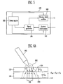
- FIG. 5 is a block diagram illustrating the structure of an active stylus according to one embodiment of the present invention. The outward appearance of the active stylus is not illustrated. However, the part that contacts the touch screen panel may be made of a sharp conductor.
- an active stylus 160 includes an electric field sensor 162 for sensing an electric field generated by a driving signal applied to a driving line that makes contact with (or approaches) the active stylus, a signal generator 164 for generating a signal (e.g., a predetermined signal) for generating an additional electric field (or an active stylus electric field) corresponding to the electric field (that is, an AC voltage) an electric field emitter 166 for amplifying the signal generated by the signal generator 164 to output the amplified signal to the electric field, and a power source 168 for applying power to the electric field sensor 162, the signal generator 164, and the electric field emitter 166.
- a signal e.g., a predetermined signal
- an additional electric field or an active stylus electric field
- an electric field emitter 166 for amplifying the signal generated by the signal generator 164 to output the amplified signal to the electric field
- a power source 168 for applying power to the electric field sensor 162, the signal generator 164, and the electric field emitter
- the electric field sensor 162 may include a coil to sense the electric field generated in accordance with (or by) the application of the driving signal. That is, when the electric field sensor 162 is positioned in a region where the electric field region generated by the driving signal is formed, the electric field generates electric power in the coil and therefore the electric field may be sensed.
- the signal generator 164 when the electric field is sensed by the electric field sensor 162, the signal generator 164 generates a signal (e.g., a predetermined signal) in accordance with the electric field. That is, the signal generator may generate an AC voltage having the same phase as the driving signal to correspond to the sensed electric field.
- a signal e.g., a predetermined signal
- the signal generated by the signal generator 164 is amplified by the electric field emitter 166, which is output to the electric field through the sharp end of the active stylus 160.
- the electric field emitter 166 may be implemented by a non-inverting amplifier that maintains the phase of the generated AC voltage and that amplifies an amplitude to output the amplified amplitude (or an active stylus electric field with an amplified amplitude) or may be an inverting amplifier that inverts the phase to output an active stylus electric field with an inverted phase.
- the active stylus 160 When the active stylus 160 according to one embodiment of the present invention contacts the specific sensing cells 116 of the touch screen panel 110, contact is sensed when the driving signals are applied to the driving lines coupled to the contacted sensing cells. Therefore, other sensing cells that are coupled to the other driving lines and that do not otherwise make contact (that is, coupled to the grounded driving lines) are not affected (or do not change in mutual capacitance) and multi-touch recognition may thereby be implemented using the active stylus 160.
- FIG. 6A is a schematic cross-sectional view illustrating a sensing cell in an active stylus contact condition according to one embodiment of the present invention.
- FIGs. 6B and 6C are views schematically illustrating sensing results in accordance with driving signals applied to the sensing cells of FIG. 6A .
- the electric field output to the active stylus is amplified by the non-inverting amplifier.
- the state in which the active stylus does not make contact is the same as illustrated in FIGs. 3A and 3B , description thereof will be omitted.
- the active stylus 160 When the active stylus 160 contacts at least one sensing cell 116, the active stylus 160 senses the electric field generated by the driving signal applied to the driving line 112 that is coupled to the sensing cell 116 and amplifies/outputs an electric field corresponding to the driving signal.
- the first electric field line 220 of FIG. 6A depicts the electric field generated by applying the driving signal and the second electric field line 600 depicts the electric field output from the active stylus 160.
- the electric field output from the active stylus 160 is generated by the AC voltage output through the non-inverting amplifier.
- the AC voltage has the same phase as the driving signal to correspond to the electric field generated by the application of the driving signal to the driving line.
- the first and second electric field lines of the first and second electric fields extend from the driving line 112 and the active stylus 160, respectively, to the sensing line 114.
- a mutual capacitance C M is formed between the driving line 112 and the sensing line 114 and AC capacitance C 2 is formed between the sensing line 114 and the active stylus 160.
- the change in the mutual capacitance in the sensing cells resultantly changes the voltage carried (or applied) to the sensing line 114 coupled to the sensing cell 116.
- the driving circuit 120 sequentially provides the driving signals (for example, voltage of 3V) to the driving lines X1, X2, ..., Xn.
- the driving circuit 120 provides the driving signal to one of the driving lines X1, X2, ..., Xn, the other driving lines are grounded.
- the driving signal is applied to the first driving line X1.
- the mutual capacitances C M are formed in the plurality of sensing cells (e.g., S11, S12, ..., S1m) where the plurality of sensing lines cross the driving lines (e.g., the first driving line X1).
- the mutual capacitance increases to C M2 so that the voltage (for example, 0.5V) corresponding to the increased mutual capacitance is sensed by the sensing lines (e.g., Y1 and Y2) coupled to the sensing cells (e.g., S11 and S12) that make contact with the active stylus 160.
- the previous (or non-contact) voltages are sensed by the sensing lines coupled to the sensing cells that do not make contact or approach the active stylus.
- the active stylus 160 contacts the sensing cells S11 and S12 coupled to the first driving line X1 and that the driving signal is not applied to the first driving line X1 but to the second driving line X2.
- the active stylus 160 since the driving signal is not applied to the driving line X1 coupled to the sensing cells S11 and S12 that contact the active stylus 160, the active stylus 160 does not sense the electric field so that an additional electric field is not output by the active stylus 160.
- the active stylus 160 since the active stylus 160 is only a simple conductor (because it is not emitting an electric field), no touch is recognized. That is, the voltage (for example, 0.3V) corresponding to the mutual capacitance C M is sensed by all of the sensing lines Y1, Y2, ..., Ym. That is, erroneous detection of touch by sensing cells near, but not in contact with the active stylus 160, is reduced or avoided.
- the active stylus 160 when the active stylus 160 according to one embodiment of the present invention makes contact with or approaches the specific (or contacted) sensing cells 116 of the touch screen panel 110, the active stylus 160 only generates an additional electric field (or active stylus electric field) when the driving signals are applied to the driving lines 112 coupled to the specific (or contacted) sensing cells. Therefore, the other sensing cells coupled to the other driving lines (excluding the sensing cells that make contact with the active stylus), that is, the sensing cells coupled to the grounded driving lines, are not affected so that multi-touch recognition may be implemented using the active stylus.
- the sensing circuit 130 coupled to the sensing lines Y1, Y2, ..., Ym converts the change in the electrostatic capacitance with respect to the sensing cells S12 and S1m that make contact and the information (sensing signal) on the position to have a pattern (e.g., a predetermined pattern) through the ADC (not shown) and transmits the converted change in the electrostatic capacitance with respect to the sensing cells S12 and S1m that make contact and the information (converted sensing signal) on the position to the processor 140.
- a pattern e.g., a predetermined pattern
- one embodiment is directed toward the method of detecting the position of the sensing cell 116 in which the change in the electrostatic capacitance is generated was described with reference to FIG. 1 , description thereof is omitted.
- recognition of a plurality of contact positions with respect to the active stylus 160 that is, multi-touch recognition, may be implemented.
- FIG. 7A is a schematic cross-sectional view illustrating a sensing cell 116 under an active stylus 160 in a contact condition according to another embodiment of the present invention.
- FIG. 7B is a view schematically illustrating sensing results in accordance with driving signals applied to the sensing cells of FIG. 7A .
- the electric field output by the active stylus 160 is amplified by an inverting amplifier. Since the state in which the active stylus does not make contact is the same as illustrated in FIGs. 3A and 3B , description thereof is omitted.
- the active stylus 160 When the active stylus 160 contacts at least one sensing cell 116, the active stylus 160 senses the electric field generated by the driving signal applied to the driving line 112 and amplifies/outputs the electric field corresponding to the driving signal.
- the first electric field lines 230 of FIG. 7A depict the electric field generated by applying the driving signal to the driving lines 112 and the second electric field lines 610 depict the electric field output from the active stylus 160.
- the electric field output from the active stylus 160 is generated by the AC voltage output through the non-inverting amplifier.
- the AC voltage has a phase opposite to the driving signal to correspond to the electric field caused by the application of the driving signal.
- the first electric field line 230 extends from the driving line 112 to the sensing line 114 and the second electric field line 610 extends from the sensing line 114 to the active stylus 160.
- the direction of the second electric field line 610 is opposite to the direction of the second electric field line 600 of FIG. 6A .
- the change in the mutual capacitance in the sensing cells resultantly changes the voltage carried to the sensing line of the sensing lines 114 coupled to the sensing cell of the sensing cells 116.
- the driving circuit 120 sequentially provides the driving signals (for example, voltages of 3V) to the driving lines X1, X2, ..., Xn.
- the driving circuit 120 provides the driving signal to one of the driving lines X1, X2, ..., Xn, the other driving lines are grounded.
- the driving signal is applied to the first driving line X1.
- the mutual capacitances C M are formed in the plurality of sensing cells (e.g., S11, S12, ..., S1m) where the plurality of sensing lines cross a driving line (e.g., the first driving line X1).
- a driving line e.g., the first driving line X1
- the sensing lines e.g., Y1 and Y2
- the sensing cells e.g., S11 and S12
- the previous (or non-contact) voltage (for example, 0.3V) is sensed by the sensing lines coupled to the non-contacting sensing cells.
- the sensing circuit 130 coupled to the sensing lines Y1, Y2, ..., Ym converts the change in the electrostatic capacitance with respect to the sensing cells (e.g., S12 and S1m) that make contact and the information (sensing signal) on the position to have a pattern (or a predetermined pattern) using the ADC and transmits the converted change in the electrostatic capacitance with respect to the sensing cells (e.g., S12 and S1m) that make contact and the converted information (converted sensing signal) on the position to the processor 140.
- the sensing cells e.g., S12 and S1m
- the sensing cells e.g., S12 and S1m
- the change in the mutual capacitance generated when the finger 150 makes contact is different from the change in the mutual capacitance generated when the active stylus 160 makes contact
- the change in the mutual capacitance generated when the finger 150 makes contact and the change in the mutual capacitance generated when the active stylus 160 makes contact may be distinguished by the sensing circuit 130 and the processor 140. Therefore, various multi-touch recognition situations may be recognized.
- the finger 150 and the active stylus 160 may concurrently (e.g., simultaneously) contact the touch screen panel 110, and the contact made by the finger 150 and the contact made by the active stylus 160 may be distinguished from each other and recognized.
- such a problem may be overcome by changing the structures of the active stylus 160 and the sensing circuit 130.
- FIG. 8 is a block diagram illustrating the structure of an active stylus 160' according to another embodiment of the present invention.
- FIG. 9 is a block diagram illustrating the structure of a sensing circuit 130' according to another embodiment of the present invention.
- an active stylus 160' includes an electric field sensor 162 for sensing the electric field generated by the driving signal applied to the driving line that make contact with (or approaches) the active stylus 160', a signal generator 164 for generating a predetermined signal, that is, an AC voltage for generating an additional electric field corresponding to the sensed electric field, an electric field emitter 166 for amplifying the signal generated by the signal generator 164 to output the amplified signal (i.e., the active stylus electric field) to the electric field, a frequency converter 169 for converting the frequency of the signal generated by the signal generator 164, that is, the AC voltage, and a power source 168 for applying power to the electric field sensor 162, the signal generator 164, the electric field emitter 166, and the frequency converter 169.
- an electric field sensor 162 for sensing the electric field generated by the driving signal applied to the driving line that make contact with (or approaches) the active stylus 160'
- a signal generator 164 for generating a predetermined signal, that is, an AC voltage
- the electric field emitter 166 converts the phase of the generated AC voltage to output the AC voltage.
- additionally providing the frequency converter 169 is to reduce a problem in which it may be difficult to distinguish between contact with a finger 150 from contact with an active stylus 160 when the AC signal having a different phase from the driving signal is output through the inverting amplifier 166, since the difference between the level (for example, 0.1V) of the sensing signal by the sensing line and the level (for example, 0.2V) of the sensing signal by the contact made by the finger 150 is not significant, it may be difficult to distinguish the level (for example, 0.1 V) of the sensing signal by the sensing line from the level (for example, 0.2V) of the sensing signal by the contact made by the finger 150.
- the level of the sensed signal may be similar to the level of the sensing signal by the contact made by the finger 150, since the frequencies are different from each other, it is easier to distinguish the sensed signal generated by contact with the active stylus 160 from the sensed signal generated by the contact made by the finger 150.
- a sensing circuit may include a frequency filter for detecting the converted frequency.
- a sensing circuit 130' includes a frequency filter 134.
- the sensing circuit 130' includes a level detector 132 for detecting the levels of the sensed signals, a frequency filter 134 for filtering signals having specific frequencies among the sensed signals, and an ADC 136 for converting the sensing signals that passed through the level detector 132 and/or the frequency filter 134 into digital signals to provide the digital signals (or converted sensing signals) to the processor 140.
- the level detector 132 detects the levels of the sensing signals. Therefore, it is possible to distinguish the sensing signal when contact is made using the active stylus 160 according to the embodiment of FIG. 6 from the sensing signal when contact is made using the finger 150.
- the frequency filter 134 is implemented by a bandpass filter for a specific frequency bandwidth to filter the frequency converted by the frequency converter 169 illustrated in FIG. 8 . Therefore, the sensing signal when contact is made using the active stylus 160' according to FIGS. 7A, 7B , and 8 may be distinguished from the sensing signal when contact is performed using the finger 150.
Landscapes
- Engineering & Computer Science (AREA)
- General Engineering & Computer Science (AREA)
- Theoretical Computer Science (AREA)
- Human Computer Interaction (AREA)
- Physics & Mathematics (AREA)
- General Physics & Mathematics (AREA)
- Position Input By Displaying (AREA)
- Measurement Of Resistance Or Impedance (AREA)
Claims (16)
- Système d'écran tactile (100), comprenant :un panneau d'écran tactile (110) comprenant une pluralité de lignes de commande (112) et une pluralité de lignes de détection (114) croisant les lignes de commande, et une pluralité de cellules de détection (116) formées au niveau de régions de croisement des lignes de commande et des lignes de détection ;un circuit de commande (120) destiné à appliquer séquentiellement des signaux de commande aux lignes de commande, dans lequel, lorsque le signal de commande est fourni à l'une des lignes de commande, les autres lignes de commande sont mises à la terre ;un circuit de détection (130) destiné à détecter des premiers signaux de détection selon des changements dans les capacités mutuelles des cellules de détection, en vue de générer des seconds signaux de détection correspondant aux changements ;un processeur (140) destiné à déterminer une position tactile sur la base des seconds signaux de détection en provenance du circuit de détection ; etun stylet actif (160) séparé du panneau d'écran tactile et comprenant :un capteur de champ électrique (162) configuré de manière à détecter un champ électrique généré par le signal de commande appliqué à une ligne de commande qui entre en contact avec ou est approchée par le stylet actif, dans lequel le générateur de signal (164) est configuré de manière à générer le signal lorsque le champ électrique est détecté par le capteur de champ électrique (162), et il ne génère pas le signal lorsque le champ électrique n'a pas été détecté par le capteur de champ électrique (162), de sorte que le générateur de signal ne génère le signal que lorsque le signal de commande est appliqué à la ligne de commande qui entre en contact avec ou est approchée par le stylet actif, et qu'il ne génère pas le signal lorsque le signal de commande n'est pas appliqué à la ligne de commande qui entre en contact avec ou est approchée par le stylet actif.un générateur de signal (164) configuré de manière à générer un signal selon le champ électrique généré par le signal de commande ;un émetteur de champ électrique (166) configuré de manière à amplifier le signal généré par le générateur de signal, en vue de générer en sortie un champ électrique de stylet actif ; etune source d'alimentation (168) configurée de manière à alimenter en énergie le générateur de signal et l'émetteur de champ électrique ;
- Système d'écran tactile selon la revendication 1, dans lequel le signal généré par le générateur de signal (164) est une tension en courant alternatif présentant la même phase que le signal de commande.
- Système d'écran tactile selon la revendication 1 ou 2, dans lequel l'émetteur de champ électrique (166) comporte un amplificateur non-inverseur destiné à maintenir la phase du signal généré par le générateur de signal (164), en vue d'amplifier le signal et de générer en sortie le champ électrique de stylet actif.
- Système d'écran tactile selon la revendication 1 ou 2, dans lequel l'émetteur de champ électrique (166) comporte un amplificateur inverseur destiné à inverser la phase du signal généré par le générateur de signal (164), en vue de générer en sortie le champ électrique de stylet actif.
- Système d'écran tactile selon la revendication 4, dans lequel le stylet actif (160) comporte en outre un convertisseur de fréquence (169) configuré de manière à convertir la fréquence de la tension en courant alternatif générée par le générateur de signal (164).
- Système d'écran tactile selon l'une quelconque des revendications précédentes, dans lequel le circuit de détection (130) comporte :un détecteur de niveaux destiné à détecter des niveaux des premiers signaux de détection ; etun convertisseur analogique-numérique, CAN, destiné à convertir la pluralité de signaux de détection en les seconds signaux de détection, en vue de fournir les seconds signaux de détection au processeur.
- Système d'écran tactile selon la revendication 6, dans lequel le circuit de détection (130) comprend en outre un filtre de fréquence destiné à filtrer des signaux présentant une fréquence spécifique parmi les premiers signaux de détection.
- Système d'écran tactile selon la revendication 7, dans lequel le filtre de fréquence comporte un filtre passe-bande.
- Système d'écran tactile selon l'une quelconque des revendications précédentes, dans lequel la pluralité de lignes de commande (112) et la pluralité de lignes de détection (114) sont situées sur différentes couches sur un substrat transparent, avec une couche isolante interposée entre celles-ci, et comportent un matériau conducteur transparent.
- Système d'écran tactile selon l'une quelconque des revendications précédentes, dans lequel les capacités mutuelles sont formées dans les cellules de détection (116), au niveau de régions de croisement entre les lignes de commande (112) et les lignes de détection (114).
- Système d'écran tactile selon la revendication 10, dans lequel les cellules de détection (116) sont configurées de manière à fournir les signaux de détection correspondant à leurs capacités mutuelles aux lignes de détection (114) auxquelles elles sont couplées, lorsque des signaux de commande sont appliqués du circuit de commande (120) aux lignes de commande (112) couplées aux cellules de détection.
- Procédé de commande d'un système d'écran tactile, comprenant les étapes ci-dessous consistant à :mettre en contact ou approcher au moins une cellule de détection parmi une pluralité de cellules de détection (116) formées au niveau de régions de croisement de lignes de commande (112) et de lignes de détection (114) d'un panneau d'écran tactile (110), avec un stylet actif (160) ;appliquer séquentiellement des signaux de commande aux lignes de commande, dans lequel, lorsque le signal de commande est fourni à l'une des lignes de commande, les autres lignes de commande sont mises à la terre ;détecter, au sein du stylet actif (160) :un champ électrique généré lorsque le signal de commande est appliqué à la ligne de commande couplée à ladite au moins une cellule de détection de laquelle le stylet actif s'approche ou avec laquelle il entre en contact ;générer, au sein du stylet actif (160) :une tension en courant alternatif correspondant au champ électrique détecté ;amplifier, au sein du stylet actif (160) :la tension en courant alternatif en vue de générer un champ électrique de stylet actif à partir du stylet actif (160) en synchronisation avec le signal de commande appliqué à la ligne de commande, de sorte qu'une capacité mutuelle dans ladite au moins une cellule de détection change, de sorte qu'une tension ou un courant appliqué(e) à une ligne de détection des lignes de détection (114) couplées à ladite au moins une cellule de détection change ; etdéterminer une position de ladite au moins une cellule de détection en utilisant le changement de la capacité mutuelle de ladite au moins une cellule de détection, sur la base d'un changement dans la tension ou le courant reçu(e) à partir de la ligne de détection ;dans lequel la tension en courant alternatif n'est pas générée lorsque le champ électrique n'est pas détecté, de sorte que le champ électrique de stylet actif n'est généré que lorsque le signal de commande est appliqué à la ligne de commande couplée à ladite au moins une cellule de détection de laquelle le stylet actif s'approche ou avec laquelle il entre en contact, et que le champ électrique de stylet actif n'est pas généré lorsque le signal de commande n'est pas appliqué à la ligne de commande couplée à ladite au moins une cellule de détection de laquelle le stylet actif s'approche ou avec laquelle il entre en contact.
- Procédé selon la revendication 12, comprenant en outre l'étape consistant à opérer une distinction entre un changement dans la capacité mutuelle générée lorsqu'un doigt entre en contact avec ladite au moins une cellule de détection et un changement dans la capacité mutuelle générée lorsque le stylet actif entre en contact avec ladite au moins une cellule de détection, lors de la détermination de la position de ladite au moins une cellule de détection.
- Procédé selon la revendication 12 ou 13, dans lequel la tension en courant alternatif présente la même phase que le signal de commande.
- Procédé selon la revendication 12 ou 13, dans lequel la tension en courant alternatif amplifiée présente sa phase inversée qui doit être générée sortie sous la forme du champ électrique de stylet actif.
- Procédé selon la revendication 15, comprenant en outre l'étape consistant à convertir la fréquence de la tension en courant alternatif.
Applications Claiming Priority (1)
| Application Number | Priority Date | Filing Date | Title |
|---|---|---|---|
| KR1020090113936A KR101073309B1 (ko) | 2009-11-24 | 2009-11-24 | 터치 스크린 시스템 및 그 구동방법 |
Publications (3)
| Publication Number | Publication Date |
|---|---|
| EP2325736A2 EP2325736A2 (fr) | 2011-05-25 |
| EP2325736A3 EP2325736A3 (fr) | 2013-06-05 |
| EP2325736B1 true EP2325736B1 (fr) | 2016-10-26 |
Family
ID=43607901
Family Applications (1)
| Application Number | Title | Priority Date | Filing Date |
|---|---|---|---|
| EP10251292.8A Active EP2325736B1 (fr) | 2009-11-24 | 2010-07-20 | Écran tactile et son procédé de commande |
Country Status (6)
| Country | Link |
|---|---|
| US (1) | US20110122087A1 (fr) |
| EP (1) | EP2325736B1 (fr) |
| JP (1) | JP5253449B2 (fr) |
| KR (1) | KR101073309B1 (fr) |
| CN (1) | CN102073423B (fr) |
| TW (1) | TWI423090B (fr) |
Families Citing this family (142)
| Publication number | Priority date | Publication date | Assignee | Title |
|---|---|---|---|---|
| US8267781B2 (en) | 2009-01-30 | 2012-09-18 | Microsoft Corporation | Visual target tracking |
| KR101752015B1 (ko) * | 2009-05-29 | 2017-06-28 | 쓰리엠 이노베이티브 프로퍼티즈 컴파니 | 고속 멀티-터치 터치 디바이스 및 그 제어기 |
| US9417738B2 (en) * | 2009-06-12 | 2016-08-16 | Synaptics Incorporated | Untethered active pen and a method for communicating with a capacitive sensing device using the untethered active pen |
| JP2012022543A (ja) * | 2010-07-15 | 2012-02-02 | Panasonic Corp | タッチパネルシステム |
| US9176630B2 (en) * | 2010-08-30 | 2015-11-03 | Perceptive Pixel, Inc. | Localizing an electrostatic stylus within a capacitive touch sensor |
| US9239637B2 (en) * | 2010-08-30 | 2016-01-19 | Perceptive Pixel, Inc. | Systems for an electrostatic stylus within a capacitive touch sensor |
| US10019119B2 (en) * | 2010-09-09 | 2018-07-10 | 3M Innovative Properties Company | Touch sensitive device with stylus support |
| WO2012039837A1 (fr) | 2010-09-22 | 2012-03-29 | Cypress Semiconductor Corporation | Stylet capacitif destiné à un écran tactile |
| US8638307B2 (en) * | 2010-09-27 | 2014-01-28 | Blackberry Limited | Electronic device and touch-sensitive input device |
| WO2012057887A1 (fr) | 2010-10-28 | 2012-05-03 | Cypress Semiconductor Corporation | Stylet capacitif avec rejet de la paume |
| KR101219273B1 (ko) * | 2011-01-14 | 2013-01-08 | 삼성디스플레이 주식회사 | 터치 스크린 시스템 |
| KR101461157B1 (ko) | 2011-04-18 | 2014-11-13 | 삼성디스플레이 주식회사 | 터치 스크린 시스템 및 그 구동방법 |
| US8928635B2 (en) * | 2011-06-22 | 2015-01-06 | Apple Inc. | Active stylus |
| US9329703B2 (en) | 2011-06-22 | 2016-05-03 | Apple Inc. | Intelligent stylus |
| US8493360B2 (en) * | 2011-07-19 | 2013-07-23 | Cypress Semiconductor Corporation | Quadrature signal receiver using synchronized oscillator |
| US8878823B1 (en) | 2011-07-27 | 2014-11-04 | Cypress Semiconductor Corporation | Dynamic shield electrode of a stylus |
| US8797301B2 (en) | 2012-02-15 | 2014-08-05 | Cypress Semiconductor Corporation | Active stylus to host data transmitting method |
| KR101671054B1 (ko) * | 2011-09-28 | 2016-10-31 | 엠파이어 테크놀로지 디벨롭먼트 엘엘씨 | 디스플레이 디바이스의 입력들의 구별 |
| KR101434004B1 (ko) * | 2011-10-21 | 2014-08-27 | 삼성전기주식회사 | 접촉 감지 장치 및 접촉 감지 방법 |
| KR101388717B1 (ko) * | 2011-10-21 | 2014-04-28 | 삼성전기주식회사 | 접촉 감지 장치 및 접촉 감지 방법 |
| KR101878882B1 (ko) * | 2011-10-21 | 2018-07-17 | 엘지디스플레이 주식회사 | 나노 메쉬 투명 전극과 이의 제조방법, 나노 메쉬 투명 전극을 포함하는 터치 스크린 및 디스플레이 장치 |
| KR101288226B1 (ko) * | 2011-10-27 | 2013-07-18 | 삼성전기주식회사 | 접촉 감지 장치 및 접촉 감지 방법 |
| US9965107B2 (en) * | 2011-10-28 | 2018-05-08 | Atmel Corporation | Authenticating with active stylus |
| US8933899B2 (en) | 2011-10-28 | 2015-01-13 | Atmel Corporation | Pulse- or frame-based communication using active stylus |
| US20130106912A1 (en) * | 2011-10-28 | 2013-05-02 | Joo Yong Um | Combination Touch-Sensor Input |
| US10162400B2 (en) * | 2011-10-28 | 2018-12-25 | Wacom Co., Ltd. | Power management system for active stylus |
| US9280218B2 (en) | 2011-10-28 | 2016-03-08 | Atmel Corporation | Modulating drive signal for communication between active stylus and touch-sensor device |
| KR101398322B1 (ko) * | 2011-12-05 | 2014-05-23 | 엘지디스플레이 주식회사 | 터치 스크린의 센싱 장치 및 방법 |
| KR101394159B1 (ko) * | 2011-12-28 | 2014-05-15 | 주식회사 실리콘웍스 | 수신 주파수 밴드를 조절할 수 있는 터치감지회로 및 상기 터치감지회로를 구비하는 터치감지시스템 |
| CN102566800B (zh) * | 2011-12-29 | 2015-08-12 | 敦泰科技有限公司 | 一种触摸笔、触摸检测方法和触摸检测系统 |
| KR101878183B1 (ko) * | 2011-12-29 | 2018-07-16 | 엘지디스플레이 주식회사 | 터치표시장치 |
| US9110543B1 (en) * | 2012-01-06 | 2015-08-18 | Steve Dabell | Method and apparatus for emulating touch and gesture events on a capacitive touch sensor |
| KR101338285B1 (ko) * | 2012-01-12 | 2013-12-09 | 주식회사 하이딥 | 터치 패널에서 터치를 감지하기 위한 방법, 장치 및 컴퓨터 판독 가능 기록 매체 |
| KR101859515B1 (ko) | 2012-02-14 | 2018-05-21 | 삼성디스플레이 주식회사 | 터치 패널 |
| US10228780B2 (en) * | 2012-02-15 | 2019-03-12 | Wacom Co., Ltd. | Stylus to host synchronization using a magnetic field |
| KR101883927B1 (ko) * | 2012-02-17 | 2018-08-02 | 삼성디스플레이 주식회사 | 터치 스크린 시스템 및 그 구동방법 |
| WO2013136763A1 (fr) * | 2012-03-12 | 2013-09-19 | パナソニック株式会社 | Stylet et système de panneau tactile équipé du stylet |
| TWI498778B (zh) * | 2012-03-19 | 2015-09-01 | Wistron Corp | 校正不同觸控系統的方法 |
| CN102662540B (zh) * | 2012-03-23 | 2015-03-11 | 旭曜科技股份有限公司 | 电容式多点触控系统的驱动频率挑选方法 |
| JP5250135B1 (ja) * | 2012-04-26 | 2013-07-31 | シャープ株式会社 | タッチパネルシステム、電子情報機器及び指示体位置検出方法 |
| WO2013169875A2 (fr) | 2012-05-09 | 2013-11-14 | Yknots Industries Llc | Dispositif, méthode et interface utilisateur graphique d'affichage de contenu associé à une affordance correspondante |
| WO2013169845A1 (fr) | 2012-05-09 | 2013-11-14 | Yknots Industries Llc | Dispositif, procédé et interface graphique utilisateur pour faire défiler des régions imbriquées |
| CN107977084B (zh) | 2012-05-09 | 2021-11-05 | 苹果公司 | 用于针对在用户界面中执行的操作提供触觉反馈的方法和装置 |
| WO2013169882A2 (fr) | 2012-05-09 | 2013-11-14 | Yknots Industries Llc | Dispositif, méthode et interface utilisateur graphique pour déplacer et déposer un objet d'interface utilisateur |
| EP2847660B1 (fr) | 2012-05-09 | 2018-11-14 | Apple Inc. | Dispositif, méthode et interface utilisateur graphique de sélection d'objets d'interface utilisateur |
| JP6273263B2 (ja) | 2012-05-09 | 2018-01-31 | アップル インコーポレイテッド | ユーザ接触に応答して追加情報を表示するための、デバイス、方法、及びグラフィカルユーザインタフェース |
| WO2013169865A2 (fr) | 2012-05-09 | 2013-11-14 | Yknots Industries Llc | Dispositif, procédé et interface d'utilisateur graphique pour déplacer un objet d'interface d'utilisateur en fonction d'une intensité d'une entrée d'appui |
| WO2013169851A2 (fr) | 2012-05-09 | 2013-11-14 | Yknots Industries Llc | Dispositif, procédé et interface d'utilisateur graphique pour faciliter l'interaction de l'utilisateur avec des commandes dans une interface d'utilisateur |
| WO2013169849A2 (fr) | 2012-05-09 | 2013-11-14 | Industries Llc Yknots | Dispositif, procédé et interface utilisateur graphique permettant d'afficher des objets d'interface utilisateur correspondant à une application |
| JP6002836B2 (ja) | 2012-05-09 | 2016-10-05 | アップル インコーポレイテッド | ジェスチャに応答して表示状態間を遷移するためのデバイス、方法、及びグラフィカルユーザインタフェース |
| CN109298789B (zh) | 2012-05-09 | 2021-12-31 | 苹果公司 | 用于针对激活状态提供反馈的设备、方法和图形用户界面 |
| WO2013169842A2 (fr) | 2012-05-09 | 2013-11-14 | Yknots Industries Llc | Dispositif, procédé, et interface utilisateur graphique permettant de sélectionner un objet parmi un groupe d'objets |
| WO2013169843A1 (fr) | 2012-05-09 | 2013-11-14 | Yknots Industries Llc | Dispositif, procédé et interface graphique utilisateur pour manipuler des objets graphiques encadrés |
| US10379666B2 (en) | 2012-05-11 | 2019-08-13 | Samsung Electronics Co., Ltd. | Position measuring apparatus, pen and position measuring method |
| KR102066017B1 (ko) * | 2012-05-11 | 2020-01-14 | 삼성전자주식회사 | 좌표 표시 장치 및 좌표 표시 장치의 입력 위치를 측정하는 좌표 측정 장치 |
| WO2013183925A1 (fr) * | 2012-06-04 | 2013-12-12 | 크루셜텍 주식회사 | Procédé et appareil de détection de toucher |
| KR101929427B1 (ko) | 2012-06-14 | 2018-12-17 | 삼성디스플레이 주식회사 | 터치 센서를 포함하는 표시 장치 |
| KR101366227B1 (ko) * | 2012-06-18 | 2014-02-24 | 다믈멀티미디어주식회사 | 스타일러스 펜, 이의 동작 방법 및 이를 포함하는 시스템 |
| TWI463388B (zh) * | 2012-06-20 | 2014-12-01 | Orise Technology Co Ltd | 增進電容式多點觸控系統的觸碰座標計算準確度之方法及電容式多點觸控系統 |
| TWI490762B (zh) * | 2012-06-29 | 2015-07-01 | Raydium Semiconductor Corp | 觸控感測裝置及觸控感測方法 |
| KR101391243B1 (ko) | 2012-07-17 | 2014-05-02 | 삼성디스플레이 주식회사 | 터치 인식 기능을 가지는 표시장치 |
| US9652090B2 (en) | 2012-07-27 | 2017-05-16 | Apple Inc. | Device for digital communication through capacitive coupling |
| US9176604B2 (en) | 2012-07-27 | 2015-11-03 | Apple Inc. | Stylus device |
| WO2014019124A1 (fr) * | 2012-07-30 | 2014-02-06 | 华为终端有限公司 | Procédé de signalement d'événement tactile, dispositif et terminal mobile |
| KR20140017255A (ko) * | 2012-07-31 | 2014-02-11 | 삼성전자주식회사 | C―type tsp을 이용한 전자펜 입력 인식 장치 및 방법 |
| US9354737B2 (en) * | 2012-08-09 | 2016-05-31 | Atmel Corporation | Active stylus self-capacitance measurement |
| US10095358B2 (en) * | 2012-08-14 | 2018-10-09 | Synaptics Incorporated | Method for driving touch sensor to achieve faster sensor settling |
| US9563304B2 (en) * | 2012-08-15 | 2017-02-07 | Atmel Corporation | Active stylus with passive mutual measurements |
| CN103294295B (zh) | 2012-08-23 | 2016-05-04 | 上海天马微电子有限公司 | 一种互感式电容性触摸屏 |
| KR101452042B1 (ko) * | 2012-09-14 | 2014-10-21 | 삼성전기주식회사 | 터치스크린 패널 및 터치스크린 장치 |
| US11314368B2 (en) | 2012-09-14 | 2022-04-26 | Samsung Display Co., Ltd. | Display device and method of driving the same in two modes |
| US9389737B2 (en) | 2012-09-14 | 2016-07-12 | Samsung Display Co., Ltd. | Display device and method of driving the same in two modes |
| KR101470903B1 (ko) | 2012-10-18 | 2014-12-09 | 주식회사 하이딥 | 터치 스크린 제어 장치 및 그의 제어 방법 |
| CN103268162B (zh) * | 2012-11-27 | 2017-05-10 | 上海天马微电子有限公司 | 一种触摸信号扫描装置及扫描方法 |
| KR101742808B1 (ko) | 2012-12-29 | 2017-06-01 | 애플 인크. | 사용자 인터페이스 계층을 내비게이션하기 위한 디바이스, 방법 및 그래픽 사용자 인터페이스 |
| WO2014105279A1 (fr) | 2012-12-29 | 2014-07-03 | Yknots Industries Llc | Dispositif, procédé et interface utilisateur graphique pour une commutation entre des interfaces utilisateur |
| EP2939096B1 (fr) | 2012-12-29 | 2019-08-28 | Apple Inc. | Dispositif, procédé et interface utilisateur graphique pour déterminer l'opportunité de faire défiler ou de sélectionner des contenus |
| WO2014105275A1 (fr) | 2012-12-29 | 2014-07-03 | Yknots Industries Llc | Dispositif, procédé et interface utilisateur graphique pour renoncer à la génération d'une sortie tactile pour un geste à contacts multiples |
| JP6158947B2 (ja) | 2012-12-29 | 2017-07-05 | アップル インコーポレイテッド | タッチ入力からディスプレイ出力への関係間を遷移するためのデバイス、方法及びグラフィカルユーザインタフェース |
| CN105144057B (zh) | 2012-12-29 | 2019-05-17 | 苹果公司 | 用于根据具有模拟三维特征的控制图标的外观变化来移动光标的设备、方法和图形用户界面 |
| KR101439855B1 (ko) * | 2013-01-25 | 2014-09-17 | 주식회사 하이딥 | 터치 스크린 제어 장치 및 그의 제어 방법 |
| KR102058437B1 (ko) * | 2013-02-25 | 2019-12-26 | 삼성전자주식회사 | 필터 값 추출기를 포함하는 터치 감지 장치 및 필터 값 추출기 |
| US10048775B2 (en) | 2013-03-14 | 2018-08-14 | Apple Inc. | Stylus detection and demodulation |
| KR20140114242A (ko) | 2013-03-18 | 2014-09-26 | 삼성전자주식회사 | 사용자 단말에서 사용자 인터페이스 장치 및 방법 |
| CN103793082A (zh) * | 2013-04-24 | 2014-05-14 | 深圳市国显科技股份有限公司 | 一种毛笔式电容笔及其触控系统 |
| KR102089607B1 (ko) | 2013-05-28 | 2020-03-17 | 삼성디스플레이 주식회사 | 표시장치 |
| TWI501132B (zh) * | 2013-07-02 | 2015-09-21 | 敦泰電子股份有限公司 | 低複雜度單層透明電極圖案之觸控面板及其感測方法 |
| CN103294279B (zh) * | 2013-07-03 | 2016-04-06 | 旭曜科技股份有限公司 | 低复杂度单层透明电极图案的触控面板及其感测方法 |
| KR102209910B1 (ko) | 2013-07-04 | 2021-02-01 | 삼성전자주식회사 | 위치 표시 장치의 입력 위치를 측정하는 위치 측정 장치 및 그 제어 방법 |
| US10209816B2 (en) | 2013-07-04 | 2019-02-19 | Samsung Electronics Co., Ltd | Coordinate measuring apparatus for measuring input position of a touch and a coordinate indicating apparatus and driving method thereof |
| US10845901B2 (en) | 2013-07-31 | 2020-11-24 | Apple Inc. | Touch controller architecture |
| JP6087244B2 (ja) * | 2013-09-04 | 2017-03-01 | アルパイン株式会社 | 位置検出装置 |
| CN103472965B (zh) * | 2013-09-13 | 2019-02-26 | 北京京东方光电科技有限公司 | 一种阵列基板及触控显示装置 |
| US9665206B1 (en) | 2013-09-18 | 2017-05-30 | Apple Inc. | Dynamic user interface adaptable to multiple input tools |
| US9459367B2 (en) | 2013-10-02 | 2016-10-04 | Synaptics Incorporated | Capacitive sensor driving technique that enables hybrid sensing or equalization |
| US8823399B1 (en) * | 2013-10-07 | 2014-09-02 | Cypress Semiconductor Corporation | Detect and differentiate touches from different size conductive objects on a capacitive button |
| KR101394465B1 (ko) * | 2013-10-15 | 2014-05-13 | 주식회사 아나패스 | 터치 감지 장치 구동 방법 및 이를 이용한 터치 감지 장치 |
| KR101535426B1 (ko) * | 2013-11-06 | 2015-07-14 | 한국표준과학연구원 | 정전용량의 변화를 이용하여 접촉 위치 및 힘 측정의 인식 감도가 개선된 정전용량형 터치 패널 및 그 측정방법 |
| KR101512571B1 (ko) | 2013-12-30 | 2015-04-15 | 삼성전기주식회사 | 접촉 감지 장치 및 터치스크린 장치 |
| KR102186393B1 (ko) | 2014-01-02 | 2020-12-03 | 삼성전자주식회사 | 입력 처리 방법 및 그 전자 장치 |
| KR102219042B1 (ko) | 2014-02-26 | 2021-02-23 | 삼성전자주식회사 | 전자 장치, 웨어러블 디바이스 및 전자 장치의 동작 방법 |
| US9690397B2 (en) * | 2014-05-20 | 2017-06-27 | Synaptics Incorporated | System and method for detecting an active pen with a matrix sensor |
| KR102248878B1 (ko) * | 2014-05-28 | 2021-05-07 | 엘지디스플레이 주식회사 | 터치 센싱 시스템 |
| KR20160017552A (ko) | 2014-08-06 | 2016-02-16 | 삼성전기주식회사 | 터치스크린 장치 및 이를 구비하는 전자 기기 |
| US9679182B2 (en) | 2014-11-12 | 2017-06-13 | Crucialtec Co., Ltd. | Display apparatus capable of image scanning and driving method thereof |
| WO2016076592A1 (fr) * | 2014-11-12 | 2016-05-19 | 크루셜텍(주) | Procédé de commande d'un dispositif d'affichage apte à numériser une image |
| KR20160056759A (ko) * | 2014-11-12 | 2016-05-20 | 크루셜텍 (주) | 이미지 스캔이 가능한 플렉서블 디스플레이 장치 및 이의 구동 방법 |
| US10180736B2 (en) * | 2014-11-26 | 2019-01-15 | Synaptics Incorporated | Pen with inductor |
| US9946391B2 (en) | 2014-11-26 | 2018-04-17 | Synaptics Incorporated | Sensing objects using multiple transmitter frequencies |
| US10088922B2 (en) | 2014-11-26 | 2018-10-02 | Synaptics Incorporated | Smart resonating pen |
| US10061450B2 (en) | 2014-12-04 | 2018-08-28 | Apple Inc. | Coarse scan and targeted active mode scan for touch |
| KR102260599B1 (ko) * | 2014-12-30 | 2021-06-04 | 엘지디스플레이 주식회사 | 터치 디스플레이 장치의 구동 방법 |
| KR101659036B1 (ko) | 2015-02-04 | 2016-09-23 | 엘지전자 주식회사 | 스타일러스 펜 및 터치 패널을 포함하는 이동 단말기 및 그 제어방법 |
| CN104636650A (zh) * | 2015-02-05 | 2015-05-20 | 惠州Tcl移动通信有限公司 | 滑动式电容指纹识别方法、系统及其系统的解锁方法 |
| US10095396B2 (en) | 2015-03-08 | 2018-10-09 | Apple Inc. | Devices, methods, and graphical user interfaces for interacting with a control object while dragging another object |
| US10048757B2 (en) | 2015-03-08 | 2018-08-14 | Apple Inc. | Devices and methods for controlling media presentation |
| US9645732B2 (en) | 2015-03-08 | 2017-05-09 | Apple Inc. | Devices, methods, and graphical user interfaces for displaying and using menus |
| US9696861B2 (en) * | 2015-03-09 | 2017-07-04 | Stmicroelectronics Asia Pacific Pte Ltd | Touch rejection for communication between a touch screen device and an active stylus |
| US9785305B2 (en) | 2015-03-19 | 2017-10-10 | Apple Inc. | Touch input cursor manipulation |
| US10055047B2 (en) | 2015-03-26 | 2018-08-21 | Himax Technologies Limited | Driver integrated circuit, driving method, and touch display system |
| US20170045981A1 (en) | 2015-08-10 | 2017-02-16 | Apple Inc. | Devices and Methods for Processing Touch Inputs Based on Their Intensities |
| WO2016163315A1 (fr) * | 2015-04-09 | 2016-10-13 | 株式会社ワコム | Procédé utilisant un stylet actif et un contrôleur de capteur, système, contrôleur de capteur et stylet actif |
| JP2016224808A (ja) * | 2015-06-02 | 2016-12-28 | 株式会社ジャパンディスプレイ | タッチ検出機能付き表示システム |
| US9860451B2 (en) | 2015-06-07 | 2018-01-02 | Apple Inc. | Devices and methods for capturing and interacting with enhanced digital images |
| US9674426B2 (en) | 2015-06-07 | 2017-06-06 | Apple Inc. | Devices and methods for capturing and interacting with enhanced digital images |
| KR101909515B1 (ko) * | 2015-06-22 | 2018-10-18 | 시그마센스, 엘엘씨. | 개선된 성능을 위해 동시적인 기능들을 사용하는 다중 터치 센서 및 정전기 펜 디지타이징 시스템 |
| KR102514046B1 (ko) * | 2015-06-22 | 2023-03-24 | 삼성전자주식회사 | 터치 스크린 컨트롤러, 터치 센싱 장치, 및 터치 센싱 방법 |
| CN105044504B (zh) * | 2015-07-08 | 2017-09-22 | 柳州利元光电技术有限公司 | 用于检测液晶显示触摸一体屏触摸电路的检测仪 |
| WO2017048061A1 (fr) * | 2015-09-18 | 2017-03-23 | Samsung Electronics Co., Ltd. | Appareil de mesure de coordonnées et procédé de commande correspondant |
| US10474280B2 (en) | 2015-12-31 | 2019-11-12 | Lg Display Co., Ltd. | Touch sensing system including active stylus pen |
| KR102523154B1 (ko) * | 2016-04-22 | 2023-04-21 | 삼성전자주식회사 | 터치 스크린 장치, 입력 장치 및 그 제어 방법 |
| US10474277B2 (en) | 2016-05-31 | 2019-11-12 | Apple Inc. | Position-based stylus communication |
| US10025403B2 (en) | 2016-07-25 | 2018-07-17 | Microsoft Technology Licensing, Llc | Stylus communication channels |
| CN109151152A (zh) * | 2017-06-19 | 2019-01-04 | 北京小米移动软件有限公司 | 电子设备的防误触方法及装置、电子设备、存储介质 |
| KR102410015B1 (ko) | 2017-12-27 | 2022-06-16 | 삼성전자주식회사 | 터치 스크린 컨트롤러, 이를 포함하는 터치 스크린 시스템 및 터치 스크린 컨트롤러의 동작방법 |
| CN109067966B (zh) * | 2018-06-15 | 2021-01-29 | Oppo广东移动通信有限公司 | 接近检测方法及相关设备 |
| US11886656B2 (en) * | 2019-04-10 | 2024-01-30 | Hideep Inc. | Electronic device and control method therefor |
| US11054920B2 (en) * | 2019-06-10 | 2021-07-06 | Sigmasense, Llc. | Pen for use with a touch screen |
| US11126297B2 (en) | 2019-06-10 | 2021-09-21 | Sigmasense, Llc. | Electronic pen with ring-back and other functionalities |
| KR102883036B1 (ko) * | 2019-12-04 | 2025-11-10 | 삼성디스플레이 주식회사 | 표시장치 및 이를 포함하는 휴대용 단말기 |
| US12153764B1 (en) | 2020-09-25 | 2024-11-26 | Apple Inc. | Stylus with receive architecture for position determination |
| CN115000655B (zh) * | 2022-03-21 | 2023-04-07 | 浙江大学 | 一种基于微带滤波器的触摸感应装置和方法 |
Family Cites Families (12)
| Publication number | Priority date | Publication date | Assignee | Title |
|---|---|---|---|---|
| JP2578005B2 (ja) * | 1990-01-06 | 1997-02-05 | グラフテック株式会社 | コードレスタブレット |
| JPH058639U (ja) * | 1991-07-18 | 1993-02-05 | グラフテツク株式会社 | コードレスタブレツトの位置指示器 |
| US5369227A (en) * | 1992-07-22 | 1994-11-29 | Summagraphics Corporation | Stylus switch status determination in a digitizer tablet having a cordless stylus |
| TW274598B (en) * | 1994-11-15 | 1996-04-21 | Alps Electric Co Ltd | Coordinate input device for pen of finger tip |
| JPH08137607A (ja) * | 1994-11-15 | 1996-05-31 | Alps Electric Co Ltd | 座標入力装置 |
| TW532679U (en) | 2001-12-20 | 2003-05-11 | Ace Cad Entpr Co Ltd | Mobile phone pen-type input device |
| KR100683249B1 (ko) * | 2005-06-16 | 2007-02-15 | 주식회사 애트랩 | 접촉센서 및 이의 신호 발생 방법 |
| GB2428306B (en) * | 2005-07-08 | 2007-09-26 | Harald Philipp | Two-dimensional capacitive position sensor |
| EP1922602A2 (fr) * | 2005-08-11 | 2008-05-21 | N-trig Ltd. | Appareil permettant de detecter des informations d'objet et ses procedes d'utilisation |
| US7612767B1 (en) * | 2005-08-24 | 2009-11-03 | Griffin Technology, Inc. | Trackpad pen for use with computer touchpad |
| JP2007183809A (ja) * | 2006-01-06 | 2007-07-19 | Sony Corp | スタイラス入力装置およびスタイラス入力方法 |
| US8482545B2 (en) * | 2008-10-02 | 2013-07-09 | Wacom Co., Ltd. | Combination touch and transducer input system and method |
-
2009
- 2009-11-24 KR KR1020090113936A patent/KR101073309B1/ko active Active
-
2010
- 2010-05-06 JP JP2010106607A patent/JP5253449B2/ja active Active
- 2010-05-19 US US12/783,473 patent/US20110122087A1/en not_active Abandoned
- 2010-06-23 CN CN201010213464.2A patent/CN102073423B/zh active Active
- 2010-06-23 TW TW099120348A patent/TWI423090B/zh active
- 2010-07-20 EP EP10251292.8A patent/EP2325736B1/fr active Active
Also Published As
| Publication number | Publication date |
|---|---|
| EP2325736A3 (fr) | 2013-06-05 |
| TW201118682A (en) | 2011-06-01 |
| JP5253449B2 (ja) | 2013-07-31 |
| KR20110057501A (ko) | 2011-06-01 |
| EP2325736A2 (fr) | 2011-05-25 |
| CN102073423B (zh) | 2016-05-25 |
| KR101073309B1 (ko) | 2011-10-12 |
| US20110122087A1 (en) | 2011-05-26 |
| CN102073423A (zh) | 2011-05-25 |
| TWI423090B (zh) | 2014-01-11 |
| JP2011113558A (ja) | 2011-06-09 |
Similar Documents
| Publication | Publication Date | Title |
|---|---|---|
| EP2325736A2 (fr) | Écran tactile et son procédé de commande | |
| KR101710559B1 (ko) | 능동 스타일러스 | |
| EP2477102B1 (fr) | Système d'écran tactile | |
| US9367168B2 (en) | Touch screen system and method of driving the same | |
| CN104951124B (zh) | 触摸检测方法及执行其的触摸检测器 | |
| US9069417B2 (en) | Hover and touch detection for digitizer | |
| US9280245B2 (en) | Touch panel sensor having dual-mode capacitive sensing for detecting an object | |
| EP3495932B1 (fr) | Appareil indicateur de coordonnées et appareil de mesure de coordonnées pour mesurer la position d'entrée de l'appareil indicateur de coordonnées | |
| US20120169631A1 (en) | Touch screen panel and driving method thereof | |
| KR20160025440A (ko) | 터치 패널 및 이를 구비한 좌표 측정 시스템 | |
| CN103941889B (zh) | 电容笔、电容触控面板和触控装置 | |
| US10055033B2 (en) | Active capacitive pen, and touch detection and feedback driving methods therefor | |
| KR102107786B1 (ko) | 터치 스크린 시스템 | |
| KR101883927B1 (ko) | 터치 스크린 시스템 및 그 구동방법 |
Legal Events
| Date | Code | Title | Description |
|---|---|---|---|
| PUAI | Public reference made under article 153(3) epc to a published international application that has entered the european phase |
Free format text: ORIGINAL CODE: 0009012 |
|
| 17P | Request for examination filed |
Effective date: 20100730 |
|
| AK | Designated contracting states |
Kind code of ref document: A2 Designated state(s): AL AT BE BG CH CY CZ DE DK EE ES FI FR GB GR HR HU IE IS IT LI LT LU LV MC MK MT NL NO PL PT RO SE SI SK SM TR |
|
| AX | Request for extension of the european patent |
Extension state: BA ME RS |
|
| RAP1 | Party data changed (applicant data changed or rights of an application transferred) |
Owner name: SAMSUNG DISPLAY CO., LTD. |
|
| PUAL | Search report despatched |
Free format text: ORIGINAL CODE: 0009013 |
|
| AK | Designated contracting states |
Kind code of ref document: A3 Designated state(s): AL AT BE BG CH CY CZ DE DK EE ES FI FR GB GR HR HU IE IS IT LI LT LU LV MC MK MT NL NO PL PT RO SE SI SK SM TR |
|
| AX | Request for extension of the european patent |
Extension state: BA ME RS |
|
| RIC1 | Information provided on ipc code assigned before grant |
Ipc: G06F 3/033 20130101ALN20130426BHEP Ipc: G06F 3/044 20060101AFI20130426BHEP |
|
| RBV | Designated contracting states (corrected) |
Designated state(s): AL AT BE BG CH CY CZ DE DK EE ES FI FR GB GR HR HU IE IS IT LI LT LU LV MC MK MT NL NO PL PT RO SE SI SK SM TR |
|
| RAP1 | Party data changed (applicant data changed or rights of an application transferred) |
Owner name: SAMSUNG DISPLAY CO., LTD. |
|
| 17Q | First examination report despatched |
Effective date: 20160115 |
|
| GRAP | Despatch of communication of intention to grant a patent |
Free format text: ORIGINAL CODE: EPIDOSNIGR1 |
|
| RIC1 | Information provided on ipc code assigned before grant |
Ipc: G06F 3/0354 20130101ALN20160415BHEP Ipc: G06F 3/044 20060101AFI20160415BHEP |
|
| INTG | Intention to grant announced |
Effective date: 20160506 |
|
| GRAS | Grant fee paid |
Free format text: ORIGINAL CODE: EPIDOSNIGR3 |
|
| GRAA | (expected) grant |
Free format text: ORIGINAL CODE: 0009210 |
|
| AK | Designated contracting states |
Kind code of ref document: B1 Designated state(s): AL AT BE BG CH CY CZ DE DK EE ES FI FR GB GR HR HU IE IS IT LI LT LU LV MC MK MT NL NO PL PT RO SE SI SK SM TR |
|
| REG | Reference to a national code |
Ref country code: GB Ref legal event code: FG4D |
|
| REG | Reference to a national code |
Ref country code: CH Ref legal event code: EP |
|
| REG | Reference to a national code |
Ref country code: AT Ref legal event code: REF Ref document number: 840462 Country of ref document: AT Kind code of ref document: T Effective date: 20161115 |
|
| REG | Reference to a national code |
Ref country code: IE Ref legal event code: FG4D |
|
| REG | Reference to a national code |
Ref country code: DE Ref legal event code: R096 Ref document number: 602010037432 Country of ref document: DE |
|
| REG | Reference to a national code |
Ref country code: LT Ref legal event code: MG4D |
|
| PG25 | Lapsed in a contracting state [announced via postgrant information from national office to epo] |
Ref country code: LV Free format text: LAPSE BECAUSE OF FAILURE TO SUBMIT A TRANSLATION OF THE DESCRIPTION OR TO PAY THE FEE WITHIN THE PRESCRIBED TIME-LIMIT Effective date: 20161026 |
|
| REG | Reference to a national code |
Ref country code: NL Ref legal event code: MP Effective date: 20161026 |
|
| REG | Reference to a national code |
Ref country code: AT Ref legal event code: MK05 Ref document number: 840462 Country of ref document: AT Kind code of ref document: T Effective date: 20161026 |
|
| PG25 | Lapsed in a contracting state [announced via postgrant information from national office to epo] |
Ref country code: LT Free format text: LAPSE BECAUSE OF FAILURE TO SUBMIT A TRANSLATION OF THE DESCRIPTION OR TO PAY THE FEE WITHIN THE PRESCRIBED TIME-LIMIT Effective date: 20161026 Ref country code: NO Free format text: LAPSE BECAUSE OF FAILURE TO SUBMIT A TRANSLATION OF THE DESCRIPTION OR TO PAY THE FEE WITHIN THE PRESCRIBED TIME-LIMIT Effective date: 20170126 Ref country code: SE Free format text: LAPSE BECAUSE OF FAILURE TO SUBMIT A TRANSLATION OF THE DESCRIPTION OR TO PAY THE FEE WITHIN THE PRESCRIBED TIME-LIMIT Effective date: 20161026 Ref country code: GR Free format text: LAPSE BECAUSE OF FAILURE TO SUBMIT A TRANSLATION OF THE DESCRIPTION OR TO PAY THE FEE WITHIN THE PRESCRIBED TIME-LIMIT Effective date: 20170127 |
|
| PG25 | Lapsed in a contracting state [announced via postgrant information from national office to epo] |
Ref country code: ES Free format text: LAPSE BECAUSE OF FAILURE TO SUBMIT A TRANSLATION OF THE DESCRIPTION OR TO PAY THE FEE WITHIN THE PRESCRIBED TIME-LIMIT Effective date: 20161026 Ref country code: NL Free format text: LAPSE BECAUSE OF FAILURE TO SUBMIT A TRANSLATION OF THE DESCRIPTION OR TO PAY THE FEE WITHIN THE PRESCRIBED TIME-LIMIT Effective date: 20161026 Ref country code: FI Free format text: LAPSE BECAUSE OF FAILURE TO SUBMIT A TRANSLATION OF THE DESCRIPTION OR TO PAY THE FEE WITHIN THE PRESCRIBED TIME-LIMIT Effective date: 20161026 Ref country code: BE Free format text: LAPSE BECAUSE OF FAILURE TO SUBMIT A TRANSLATION OF THE DESCRIPTION OR TO PAY THE FEE WITHIN THE PRESCRIBED TIME-LIMIT Effective date: 20161026 Ref country code: PT Free format text: LAPSE BECAUSE OF FAILURE TO SUBMIT A TRANSLATION OF THE DESCRIPTION OR TO PAY THE FEE WITHIN THE PRESCRIBED TIME-LIMIT Effective date: 20170227 Ref country code: PL Free format text: LAPSE BECAUSE OF FAILURE TO SUBMIT A TRANSLATION OF THE DESCRIPTION OR TO PAY THE FEE WITHIN THE PRESCRIBED TIME-LIMIT Effective date: 20161026 Ref country code: HR Free format text: LAPSE BECAUSE OF FAILURE TO SUBMIT A TRANSLATION OF THE DESCRIPTION OR TO PAY THE FEE WITHIN THE PRESCRIBED TIME-LIMIT Effective date: 20161026 Ref country code: AT Free format text: LAPSE BECAUSE OF FAILURE TO SUBMIT A TRANSLATION OF THE DESCRIPTION OR TO PAY THE FEE WITHIN THE PRESCRIBED TIME-LIMIT Effective date: 20161026 Ref country code: IS Free format text: LAPSE BECAUSE OF FAILURE TO SUBMIT A TRANSLATION OF THE DESCRIPTION OR TO PAY THE FEE WITHIN THE PRESCRIBED TIME-LIMIT Effective date: 20170226 |
|
| REG | Reference to a national code |
Ref country code: FR Ref legal event code: PLFP Year of fee payment: 8 |
|
| REG | Reference to a national code |
Ref country code: DE Ref legal event code: R097 Ref document number: 602010037432 Country of ref document: DE |
|
| PG25 | Lapsed in a contracting state [announced via postgrant information from national office to epo] |
Ref country code: RO Free format text: LAPSE BECAUSE OF FAILURE TO SUBMIT A TRANSLATION OF THE DESCRIPTION OR TO PAY THE FEE WITHIN THE PRESCRIBED TIME-LIMIT Effective date: 20161026 Ref country code: SK Free format text: LAPSE BECAUSE OF FAILURE TO SUBMIT A TRANSLATION OF THE DESCRIPTION OR TO PAY THE FEE WITHIN THE PRESCRIBED TIME-LIMIT Effective date: 20161026 Ref country code: DK Free format text: LAPSE BECAUSE OF FAILURE TO SUBMIT A TRANSLATION OF THE DESCRIPTION OR TO PAY THE FEE WITHIN THE PRESCRIBED TIME-LIMIT Effective date: 20161026 Ref country code: CZ Free format text: LAPSE BECAUSE OF FAILURE TO SUBMIT A TRANSLATION OF THE DESCRIPTION OR TO PAY THE FEE WITHIN THE PRESCRIBED TIME-LIMIT Effective date: 20161026 Ref country code: EE Free format text: LAPSE BECAUSE OF FAILURE TO SUBMIT A TRANSLATION OF THE DESCRIPTION OR TO PAY THE FEE WITHIN THE PRESCRIBED TIME-LIMIT Effective date: 20161026 |
|
| PG25 | Lapsed in a contracting state [announced via postgrant information from national office to epo] |
Ref country code: SM Free format text: LAPSE BECAUSE OF FAILURE TO SUBMIT A TRANSLATION OF THE DESCRIPTION OR TO PAY THE FEE WITHIN THE PRESCRIBED TIME-LIMIT Effective date: 20161026 Ref country code: IT Free format text: LAPSE BECAUSE OF FAILURE TO SUBMIT A TRANSLATION OF THE DESCRIPTION OR TO PAY THE FEE WITHIN THE PRESCRIBED TIME-LIMIT Effective date: 20161026 Ref country code: BG Free format text: LAPSE BECAUSE OF FAILURE TO SUBMIT A TRANSLATION OF THE DESCRIPTION OR TO PAY THE FEE WITHIN THE PRESCRIBED TIME-LIMIT Effective date: 20170126 |
|
| PLBE | No opposition filed within time limit |
Free format text: ORIGINAL CODE: 0009261 |
|
| STAA | Information on the status of an ep patent application or granted ep patent |
Free format text: STATUS: NO OPPOSITION FILED WITHIN TIME LIMIT |
|
| 26N | No opposition filed |
Effective date: 20170727 |
|
| PG25 | Lapsed in a contracting state [announced via postgrant information from national office to epo] |
Ref country code: SI Free format text: LAPSE BECAUSE OF FAILURE TO SUBMIT A TRANSLATION OF THE DESCRIPTION OR TO PAY THE FEE WITHIN THE PRESCRIBED TIME-LIMIT Effective date: 20161026 |
|
| REG | Reference to a national code |
Ref country code: CH Ref legal event code: PL |
|
| REG | Reference to a national code |
Ref country code: IE Ref legal event code: MM4A |
|
| PG25 | Lapsed in a contracting state [announced via postgrant information from national office to epo] |
Ref country code: CH Free format text: LAPSE BECAUSE OF NON-PAYMENT OF DUE FEES Effective date: 20170731 Ref country code: IE Free format text: LAPSE BECAUSE OF NON-PAYMENT OF DUE FEES Effective date: 20170720 Ref country code: LI Free format text: LAPSE BECAUSE OF NON-PAYMENT OF DUE FEES Effective date: 20170731 |
|
| REG | Reference to a national code |
Ref country code: FR Ref legal event code: PLFP Year of fee payment: 9 |
|
| PG25 | Lapsed in a contracting state [announced via postgrant information from national office to epo] |
Ref country code: LU Free format text: LAPSE BECAUSE OF NON-PAYMENT OF DUE FEES Effective date: 20170720 |
|
| PG25 | Lapsed in a contracting state [announced via postgrant information from national office to epo] |
Ref country code: MT Free format text: LAPSE BECAUSE OF NON-PAYMENT OF DUE FEES Effective date: 20170720 |
|
| PG25 | Lapsed in a contracting state [announced via postgrant information from national office to epo] |
Ref country code: HU Free format text: LAPSE BECAUSE OF FAILURE TO SUBMIT A TRANSLATION OF THE DESCRIPTION OR TO PAY THE FEE WITHIN THE PRESCRIBED TIME-LIMIT; INVALID AB INITIO Effective date: 20100720 Ref country code: MC Free format text: LAPSE BECAUSE OF FAILURE TO SUBMIT A TRANSLATION OF THE DESCRIPTION OR TO PAY THE FEE WITHIN THE PRESCRIBED TIME-LIMIT Effective date: 20161026 |
|
| PG25 | Lapsed in a contracting state [announced via postgrant information from national office to epo] |
Ref country code: CY Free format text: LAPSE BECAUSE OF NON-PAYMENT OF DUE FEES Effective date: 20161026 |
|
| PG25 | Lapsed in a contracting state [announced via postgrant information from national office to epo] |
Ref country code: MK Free format text: LAPSE BECAUSE OF FAILURE TO SUBMIT A TRANSLATION OF THE DESCRIPTION OR TO PAY THE FEE WITHIN THE PRESCRIBED TIME-LIMIT Effective date: 20161026 |
|
| PG25 | Lapsed in a contracting state [announced via postgrant information from national office to epo] |
Ref country code: TR Free format text: LAPSE BECAUSE OF FAILURE TO SUBMIT A TRANSLATION OF THE DESCRIPTION OR TO PAY THE FEE WITHIN THE PRESCRIBED TIME-LIMIT Effective date: 20161026 |
|
| PG25 | Lapsed in a contracting state [announced via postgrant information from national office to epo] |
Ref country code: AL Free format text: LAPSE BECAUSE OF FAILURE TO SUBMIT A TRANSLATION OF THE DESCRIPTION OR TO PAY THE FEE WITHIN THE PRESCRIBED TIME-LIMIT Effective date: 20161026 |
|
| P01 | Opt-out of the competence of the unified patent court (upc) registered |
Effective date: 20230515 |
|
| PGFP | Annual fee paid to national office [announced via postgrant information from national office to epo] |
Ref country code: GB Payment date: 20250624 Year of fee payment: 16 |
|
| PGFP | Annual fee paid to national office [announced via postgrant information from national office to epo] |
Ref country code: FR Payment date: 20250624 Year of fee payment: 16 |
|
| PGFP | Annual fee paid to national office [announced via postgrant information from national office to epo] |
Ref country code: DE Payment date: 20250624 Year of fee payment: 16 |