EP2325873A1 - Verfahren zur Herstellung einer frei hängenden Membran und MOS-Transistor mit Doppel-Gate - Google Patents
Verfahren zur Herstellung einer frei hängenden Membran und MOS-Transistor mit Doppel-Gate Download PDFInfo
- Publication number
- EP2325873A1 EP2325873A1 EP10191762A EP10191762A EP2325873A1 EP 2325873 A1 EP2325873 A1 EP 2325873A1 EP 10191762 A EP10191762 A EP 10191762A EP 10191762 A EP10191762 A EP 10191762A EP 2325873 A1 EP2325873 A1 EP 2325873A1
- Authority
- EP
- European Patent Office
- Prior art keywords
- layer
- membrane
- isolation
- under
- gate
- Prior art date
- Legal status (The legal status is an assumption and is not a legal conclusion. Google has not performed a legal analysis and makes no representation as to the accuracy of the status listed.)
- Withdrawn
Links
Images


Classifications
-
- H—ELECTRICITY
- H10—SEMICONDUCTOR DEVICES; ELECTRIC SOLID-STATE DEVICES NOT OTHERWISE PROVIDED FOR
- H10D—INORGANIC ELECTRIC SEMICONDUCTOR DEVICES
- H10D30/00—Field-effect transistors [FET]
- H10D30/60—Insulated-gate field-effect transistors [IGFET]
- H10D30/67—Thin-film transistors [TFT]
- H10D30/6729—Thin-film transistors [TFT] characterised by the electrodes
- H10D30/673—Thin-film transistors [TFT] characterised by the electrodes characterised by the shapes, relative sizes or dispositions of the gate electrodes
- H10D30/6733—Multi-gate TFTs
- H10D30/6734—Multi-gate TFTs having gate electrodes arranged on both top and bottom sides of the channel, e.g. dual-gate TFTs
-
- H—ELECTRICITY
- H10—SEMICONDUCTOR DEVICES; ELECTRIC SOLID-STATE DEVICES NOT OTHERWISE PROVIDED FOR
- H10D—INORGANIC ELECTRIC SEMICONDUCTOR DEVICES
- H10D30/00—Field-effect transistors [FET]
- H10D30/60—Insulated-gate field-effect transistors [IGFET]
- H10D30/67—Thin-film transistors [TFT]
Definitions
- the present invention relates to the field of integrated circuits. It relates more particularly to the methods of manufacturing electronic components designated in the art by the acronym SON (English Silicon On None or "silicon on nothing").
- MOS transistors are commonly produced on an SOI (Silicon On Insulator) substrate.
- SOI Silicon On Insulator
- the cost of this substrate being not negligible, it has been proposed to form in a solid substrate in a localized manner a buried layer of silicon oxide under a monocrystalline silicon film on which the transistor will be made.
- the Figures 1A to 4B illustrate successive steps of producing a MOS transistor on a portion of a substrate comprising a buried silicon oxide layer.
- FIGS. 1A and 1B are respectively a top view and a sectional view along the plane BB of the Figure 1A of an initial manufacturing step.
- an isolation ring 2 has been made delimiting an active zone 4.
- the active zone 4 has been etched to a certain depth before a silicon-germanium sacrificial layer 6 and a silicon layer 8 are successively epitaxially produced to a thickness corresponding to the etching depth.
- a gate insulator 12 was deposited on the layer 8 and then formed a metal gate 10.
- the upper part of the gate comprises a polycrystalline silicon layer 14.
- Two spacers 16 are formed on either side of the gate 10-14 .
- the gate 10-14 extends on the isolation ring 2, on either side of the active zone 4.
- the isolation ring 2 was etched so as to be able to access the sacrificial layer 6. Then, the layer 6 was removed. The mechanical strength of the membrane suspended corresponding to the layer 8 is provided by the extensions of the grid 10-14 which rely on the isolation ring 2.
- a layer 22 of silicon oxide has been deposited under the layer 8. It is then possible to form in the silicon layer 8 a MOS transistor which is isolated from the substrate 1 by the Such a transistor has the same advantages as a transistor formed in the upper silicon layer of an SOI type structure.
- the selective etching of the sacrificial layer 6 with respect to the layer 8 is performed after forming the gate 10-14.
- a high temperature hydrogen chloride gas used for this step inevitably attacks the metal grid 10, which can be problematic.
- the etch selectivity is not perfect with respect to the spacers 16 and the gate insulator 12.
- An object of an embodiment of the present invention is to provide a method of manufacturing a MOS transistor on insulator avoiding at least some of the disadvantages of prior methods.
- a more general object of an embodiment of the present invention is to provide a method of manufacturing a suspended membrane simple to implement.
- a more particular object of an embodiment of the present invention is to provide a method of manufacturing a dual gate MOS transistor.
- the etching depth corresponds substantially to the depth of digging of the active zone.
- the thickness of the first layer is between 10 and 50 nm, preferably between 15 and 25 nm and the thickness of the second layer is between 2 and 20 nm, preferably between 5 and 10 nm, the etching depth being between 4 and 100 nm, preferably between 10 and 40 nm.
- the resin layer is converted to silicon oxide after the insolation step and after an annealing step.
- a gate isolation layer is formed on and under the membrane prior to deposition of the resin layer.
- a gate isolation layer is formed in the trenches on and under the membrane.
- the gate isolation layer is hafnium oxide.
- Another embodiment of the present invention provides a device comprising an active zone formed in a monocrystalline semiconductor substrate delimited by an isolation ring, the ring comprising at least two distinct thicknesses, the difference of the two thicknesses corresponding to an etching depth of a portion of the inner periphery of said ring, the active area comprising a suspended membrane whose flanks are integral with the isolation region.
- the device comprises upper and lower insulated gate conductors disposed respectively on and under the membrane, the membrane comprising source and drain regions.
- a solid substrate 1 of monocrystalline semiconductor material for example silicon
- the isolation ring 2 is for example made of silicon oxide.
- Zone 40 was then dug by partially etching the silicon, for example by a high temperature hydrogen chloride gas to a depth less than that of the isolation ring.
- a sacrificial layer 42 for example silicon-germanium, was formed by epitaxy, followed by a monocrystalline semiconductor layer 44, for example made of silicon.
- the upper surface of the layer 44 is at the upper surface of the isolation ring 2 or slightly below.
- the thickness of the sacrificial layer 42 is for example between 10 and 50 nm, preferably between 15 and 25 nm.
- the thickness of the layer 44 is for example between 2 and 20 nm, preferably between 5 and 10 nm.
- the etching depth e is greater than the thickness of the layer 44.
- the lateral accesses 46 are formed to the sacrificial layer 42.
- the etching depth e substantially corresponds to the depth of digging of the active zone 40.
- the depth e of the etching is between 4 and 100 nm, preferably between 10 and 40 nm.
- the etching of the isolation ring 2 can be done wet using for example a solution of hydrofluoric acid or by plasma using for example a plasma of C 4 H 8 .
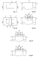
- FIGS. 7B, 7D and 7E are cross-sectional views, illustrating a step in the method of manufacturing a suspended membrane, which respectively correspond to the sections of the Figures 6B, 6D and 6E .
- the layer 44 thus constitutes a suspended membrane.
- the etching of the layer 44 was performed laterally by the accesses 46, as seen in FIG. Figure 7D .
- the suspended membrane is integral with the crown isolation 2 by the flanks 48 opposite.
- the mechanical strength of the membrane 44 is ensured by anchoring the flanks 48 in the part of the non-etched insulation ring 2.
- an insulating layer is deposited under the membrane 44.
- the insulating layer may be, for example, silicon oxide.
- CVD Chemical Vapor Deposition
- the Figures 8A to 9B illustrate steps of providing a method of forming a dual gate MOS transistor 70.
- the resin 80 is a resin of the HSQ (Hydrogen SilsesQuioxane) or PMMA resin type ( polymethylmethacrylate). After exposure by an electron beam, development and annealing of such a resin, it is transformed into silicon oxide.
- Resin 80 has been formed into an upper trench 82 on the membrane and a lower trench 84 under the membrane as seen in FIG. Figure 8B .
- the two trenches are aligned.
- the trenches open on the engraved inner periphery of the crown 2.
- two access portions 46 not filled with resin 80 allow access to the trench 84.
- the trenches 82 and 84 were made by a step of electron beam lithography or extreme ultraviolet radiation.
- the thickness of the membrane 44 advantageously between 2 and 20 nm, preferably between 5 and 10 nm, is sufficiently fine to allow irradiation by the electron beam or the extreme ultraviolet radiation of the resin 80 disposed under the membrane.
- the resin 80 was then developed, followed by a step of annealing the resin.
- a grid insulator 90 on or under the membrane 44 has been deposited or grown by the access portions 46 in each of the trenches 82 and 84.
- the gate insulator may be oxide silicon or hafnium oxide.
- a conductive material is then deposited which forms an upper insulated gate 94 above the membrane and a lower insulated gate 96 beneath the membrane.
- the upper grid 94 symbolized by simple hatching extends on the isolation ring 2 on both sides of the membrane 44, while the lower grid 96, symbolized by double hatching, extends only under the membrane 44.
- the conductive grids 94 and 96 are made of titanium nitride. As the conductor is useful only at the interface with the gate oxide, a small conductor thickness is sufficient.
- a so-called damascene method was used by depositing polycrystalline silicon on the layer 80 so as to fill the trenches 82 and 84.
- the polycrystalline silicon layer protruding from the trench 82 was chemically and mechanically polished up to layer 80 of silicon oxide constituting a barrier layer.
- the layer 80 was then removed for example by a solution of hydrofluoric acid.
- the gate isolation layer 90 is advantageously hafnium oxide. Thus, the etching of the silicon oxide layer 80 is selective with respect to the gate isolation layer 90.
- the source and drain regions were formed in the membrane 44 on either side of the channel region interposed between the two isolated grids 94 and 96.
- This method makes it possible to obtain a double-gate MOS transistor 70 whose two gates are self-aligned.
- this layer will serve as a stop layer for the etching of the layer 80.
- the grids of the double gate transistor 70 may be made integrally of polycrystalline silicon.
- the two upper insulated grids 94 and lower 96 can be interconnected following a deposition of gate material coating the membrane 44.
Landscapes
- Thin Film Transistor (AREA)
- Insulated Gate Type Field-Effect Transistor (AREA)
- Element Separation (AREA)
Applications Claiming Priority (1)
| Application Number | Priority Date | Filing Date | Title |
|---|---|---|---|
| FR0958280 | 2009-11-23 |
Publications (1)
| Publication Number | Publication Date |
|---|---|
| EP2325873A1 true EP2325873A1 (de) | 2011-05-25 |
Family
ID=42077783
Family Applications (1)
| Application Number | Title | Priority Date | Filing Date |
|---|---|---|---|
| EP10191762A Withdrawn EP2325873A1 (de) | 2009-11-23 | 2010-11-18 | Verfahren zur Herstellung einer frei hängenden Membran und MOS-Transistor mit Doppel-Gate |
Country Status (2)
| Country | Link |
|---|---|
| US (2) | US8586445B2 (de) |
| EP (1) | EP2325873A1 (de) |
Cited By (2)
| Publication number | Priority date | Publication date | Assignee | Title |
|---|---|---|---|---|
| FR2976401A1 (fr) * | 2011-06-07 | 2012-12-14 | St Microelectronics Crolles 2 | Composant electronique comportant un ensemble de transistors mosfet et procede de fabrication |
| US20150249014A1 (en) * | 2012-09-18 | 2015-09-03 | Commissariat A' L'energie Atomique Et Aux Energies Alternatives | Process for producing a double-gate field-effect device having independent gates |
Families Citing this family (2)
| Publication number | Priority date | Publication date | Assignee | Title |
|---|---|---|---|---|
| CN103730361B (zh) * | 2012-10-10 | 2018-02-13 | 中国科学院微电子研究所 | 半导体器件制造方法 |
| US9391163B2 (en) | 2014-10-03 | 2016-07-12 | International Business Machines Corporation | Stacked planar double-gate lamellar field-effect transistor |
Citations (4)
| Publication number | Priority date | Publication date | Assignee | Title |
|---|---|---|---|---|
| FR2821483A1 (fr) * | 2001-02-28 | 2002-08-30 | St Microelectronics Sa | Procede de fabrication d'un transistor a grille isolee et a architecture du type substrat sur isolant, et transistor correspondant |
| JP2007134366A (ja) * | 2005-11-08 | 2007-05-31 | Seiko Epson Corp | 半導体装置および半導体装置の製造方法 |
| FR2901058A1 (fr) * | 2006-08-29 | 2007-11-16 | St Microelectronics Crolles 2 | Dispositif a fonction dissymetrique et procede de realisation correspondant. |
| US20090032874A1 (en) * | 2007-07-05 | 2009-02-05 | Stmicroelectronics Sa | Method for integrating silicon-on-nothing devices with standard cmos devices |
Family Cites Families (3)
| Publication number | Priority date | Publication date | Assignee | Title |
|---|---|---|---|---|
| US7015147B2 (en) * | 2003-07-22 | 2006-03-21 | Sharp Laboratories Of America, Inc. | Fabrication of silicon-on-nothing (SON) MOSFET fabrication using selective etching of Si1-xGex layer |
| US7547641B2 (en) * | 2007-06-05 | 2009-06-16 | International Business Machines Corporation | Super hybrid SOI CMOS devices |
| US8835231B2 (en) * | 2010-08-16 | 2014-09-16 | International Business Machines Corporation | Methods of forming contacts for nanowire field effect transistors |
-
2010
- 2010-11-18 EP EP10191762A patent/EP2325873A1/de not_active Withdrawn
- 2010-11-18 US US12/949,286 patent/US8586445B2/en active Active
-
2013
- 2013-11-12 US US14/077,724 patent/US9184295B2/en active Active
Patent Citations (4)
| Publication number | Priority date | Publication date | Assignee | Title |
|---|---|---|---|---|
| FR2821483A1 (fr) * | 2001-02-28 | 2002-08-30 | St Microelectronics Sa | Procede de fabrication d'un transistor a grille isolee et a architecture du type substrat sur isolant, et transistor correspondant |
| JP2007134366A (ja) * | 2005-11-08 | 2007-05-31 | Seiko Epson Corp | 半導体装置および半導体装置の製造方法 |
| FR2901058A1 (fr) * | 2006-08-29 | 2007-11-16 | St Microelectronics Crolles 2 | Dispositif a fonction dissymetrique et procede de realisation correspondant. |
| US20090032874A1 (en) * | 2007-07-05 | 2009-02-05 | Stmicroelectronics Sa | Method for integrating silicon-on-nothing devices with standard cmos devices |
Cited By (3)
| Publication number | Priority date | Publication date | Assignee | Title |
|---|---|---|---|---|
| FR2976401A1 (fr) * | 2011-06-07 | 2012-12-14 | St Microelectronics Crolles 2 | Composant electronique comportant un ensemble de transistors mosfet et procede de fabrication |
| US20150249014A1 (en) * | 2012-09-18 | 2015-09-03 | Commissariat A' L'energie Atomique Et Aux Energies Alternatives | Process for producing a double-gate field-effect device having independent gates |
| US9236262B2 (en) * | 2012-09-18 | 2016-01-12 | Commissariat à l'Energie Atomique et aux Energies Alternatives | Process for producing a double-gate field-effect device having independent gates |
Also Published As
| Publication number | Publication date |
|---|---|
| US20110121391A1 (en) | 2011-05-26 |
| US8586445B2 (en) | 2013-11-19 |
| US20140070317A1 (en) | 2014-03-13 |
| US9184295B2 (en) | 2015-11-10 |
Similar Documents
| Publication | Publication Date | Title |
|---|---|---|
| EP1837916B1 (de) | Verfahren zum Herstellen eines Transistors mit einem Germanium enthaltenden Kanal | |
| EP1091417A1 (de) | Herstellungsverfahren für Halbleiterbauelement mit Rundherum-Gate und dadurch hergestelltes Bauelement | |
| FR3060840A1 (fr) | Procede de realisation d'un dispositif semi-conducteur a espaceurs internes auto-alignes | |
| FR2823010A1 (fr) | Procede de fabrication d'un transistor vertical a grille isolee a quadruple canal de conduction, et circuit integre comportant un tel transistor | |
| FR2821483A1 (fr) | Procede de fabrication d'un transistor a grille isolee et a architecture du type substrat sur isolant, et transistor correspondant | |
| FR2990295A1 (fr) | Procede de formation de contacts de grille, de source et de drain sur un transistor mos | |
| EP2610915A1 (de) | Transistor und Herstellungsverfahren eines Transistors | |
| EP1670063B1 (de) | Peripherie eines vertikalen, unipolaren Bauelementes | |
| EP2765599A1 (de) | Verfahren zur Herstellung eines Transistors | |
| EP3503175A1 (de) | Herstellungsverfahren eines halbleitersubstrats mit mindestens einem unter druckspannung stehenden halbleiterbereich | |
| EP1507286B1 (de) | Herstellungsverfahren einer Netzwerkverbindung einer integrierten Schaltung und Herstellungsverfahren eines Transistors mit umschliessendem Gate | |
| FR2547954A1 (fr) | Procede de fabrication de composants semi-conducteurs isoles dans une plaquette semi-conductrice | |
| US9184295B2 (en) | Method for manufacturing a suspended membrane and dual-gate MOS transistor | |
| FR3040538A1 (fr) | Transistor mos et son procede de fabrication | |
| FR2807873A1 (fr) | Procede de fabrication d'un dispositif a semiconducteur utilisant un substrat soi | |
| EP0675544B1 (de) | Verfahren zur Herstellung eines Feldeffekttransistors mit isoliertem Gate und kurzem Kanal, und entsprechender Transistor | |
| EP0413645B1 (de) | Verfahren zum Herstellen eines Mesa-MOS-Transistors des Typs SOI | |
| TW202113940A (zh) | Gaa電晶體中藉由選擇性頂部沉積製程之底部隔離形成方法 | |
| US6555445B2 (en) | Manufacturing method of semiconductor device | |
| FR2976401A1 (fr) | Composant electronique comportant un ensemble de transistors mosfet et procede de fabrication | |
| FR2928490A1 (fr) | Circuit integre comprenant des miroirs enterres a des profondeurs differentes | |
| EP3503203A1 (de) | Herstellung von transistoren mit unter spannung stehenden kanälen | |
| FR3076398A1 (fr) | Transistor et son procede de fabrication | |
| FR3098981A1 (fr) | procédé de fabrication de transistors | |
| FR3055469A1 (fr) | Transistor a effet de champ a grille entourante |
Legal Events
| Date | Code | Title | Description |
|---|---|---|---|
| PUAI | Public reference made under article 153(3) epc to a published international application that has entered the european phase |
Free format text: ORIGINAL CODE: 0009012 |
|
| 17P | Request for examination filed |
Effective date: 20101118 |
|
| AK | Designated contracting states |
Kind code of ref document: A1 Designated state(s): AL AT BE BG CH CY CZ DE DK EE ES FI FR GB GR HR HU IE IS IT LI LT LU LV MC MK MT NL NO PL PT RO RS SE SI SK SM TR |
|
| AX | Request for extension of the european patent |
Extension state: BA ME |
|
| 17Q | First examination report despatched |
Effective date: 20140116 |
|
| STAA | Information on the status of an ep patent application or granted ep patent |
Free format text: STATUS: THE APPLICATION IS DEEMED TO BE WITHDRAWN |
|
| 18D | Application deemed to be withdrawn |
Effective date: 20140527 |