EP2325904A2 - Réseau de micro-diodes électroluminescentes avec extraction de lumière accrue - Google Patents
Réseau de micro-diodes électroluminescentes avec extraction de lumière accrue Download PDFInfo
- Publication number
- EP2325904A2 EP2325904A2 EP10189721A EP10189721A EP2325904A2 EP 2325904 A2 EP2325904 A2 EP 2325904A2 EP 10189721 A EP10189721 A EP 10189721A EP 10189721 A EP10189721 A EP 10189721A EP 2325904 A2 EP2325904 A2 EP 2325904A2
- Authority
- EP
- European Patent Office
- Prior art keywords
- layer
- led
- spreader
- micro
- emitting elements
- Prior art date
- Legal status (The legal status is an assumption and is not a legal conclusion. Google has not performed a legal analysis and makes no representation as to the accuracy of the status listed.)
- Granted
Links
- 238000000605 extraction Methods 0.000 title claims description 18
- 239000000758 substrate Substances 0.000 claims description 34
- 239000000463 material Substances 0.000 claims description 29
- 239000004065 semiconductor Substances 0.000 claims description 26
- 230000007480 spreading Effects 0.000 claims description 24
- 238000003892 spreading Methods 0.000 claims description 24
- 239000004020 conductor Substances 0.000 claims description 5
- 238000000034 method Methods 0.000 description 24
- 229910052737 gold Inorganic materials 0.000 description 14
- 230000001965 increasing effect Effects 0.000 description 9
- 238000004519 manufacturing process Methods 0.000 description 7
- 229910052697 platinum Inorganic materials 0.000 description 7
- 238000013459 approach Methods 0.000 description 6
- 229910052751 metal Inorganic materials 0.000 description 6
- 239000002184 metal Substances 0.000 description 6
- 229910052763 palladium Inorganic materials 0.000 description 6
- 238000001020 plasma etching Methods 0.000 description 6
- 239000012212 insulator Substances 0.000 description 5
- 230000003993 interaction Effects 0.000 description 5
- 229920000642 polymer Polymers 0.000 description 5
- HBMJWWWQQXIZIP-UHFFFAOYSA-N silicon carbide Chemical compound [Si+]#[C-] HBMJWWWQQXIZIP-UHFFFAOYSA-N 0.000 description 5
- 230000008901 benefit Effects 0.000 description 4
- 238000000151 deposition Methods 0.000 description 4
- 238000005530 etching Methods 0.000 description 4
- 229910052759 nickel Inorganic materials 0.000 description 4
- 229920002120 photoresistant polymer Polymers 0.000 description 4
- 229910052594 sapphire Inorganic materials 0.000 description 4
- 239000010980 sapphire Substances 0.000 description 4
- 229910010271 silicon carbide Inorganic materials 0.000 description 4
- 229910000980 Aluminium gallium arsenide Inorganic materials 0.000 description 3
- VYPSYNLAJGMNEJ-UHFFFAOYSA-N Silicium dioxide Chemical compound O=[Si]=O VYPSYNLAJGMNEJ-UHFFFAOYSA-N 0.000 description 3
- 239000000956 alloy Substances 0.000 description 3
- 230000000903 blocking effect Effects 0.000 description 3
- 230000002708 enhancing effect Effects 0.000 description 3
- 150000004767 nitrides Chemical class 0.000 description 3
- 230000000737 periodic effect Effects 0.000 description 3
- 229910052709 silver Inorganic materials 0.000 description 3
- 238000000992 sputter etching Methods 0.000 description 3
- 238000003631 wet chemical etching Methods 0.000 description 3
- 229910001218 Gallium arsenide Inorganic materials 0.000 description 2
- 239000004793 Polystyrene Substances 0.000 description 2
- 229910045601 alloy Inorganic materials 0.000 description 2
- 238000003491 array Methods 0.000 description 2
- 230000015572 biosynthetic process Effects 0.000 description 2
- 238000001312 dry etching Methods 0.000 description 2
- 230000000694 effects Effects 0.000 description 2
- 238000001704 evaporation Methods 0.000 description 2
- 230000008020 evaporation Effects 0.000 description 2
- 239000010408 film Substances 0.000 description 2
- 238000010438 heat treatment Methods 0.000 description 2
- 238000001465 metallisation Methods 0.000 description 2
- 150000002739 metals Chemical class 0.000 description 2
- 230000003287 optical effect Effects 0.000 description 2
- 229920002223 polystyrene Polymers 0.000 description 2
- 230000008569 process Effects 0.000 description 2
- 238000000926 separation method Methods 0.000 description 2
- 238000004544 sputter deposition Methods 0.000 description 2
- 239000010409 thin film Substances 0.000 description 2
- 238000012546 transfer Methods 0.000 description 2
- 239000004593 Epoxy Substances 0.000 description 1
- 229910052774 Proactinium Inorganic materials 0.000 description 1
- 239000012080 ambient air Substances 0.000 description 1
- 238000000149 argon plasma sintering Methods 0.000 description 1
- 238000006243 chemical reaction Methods 0.000 description 1
- 229910052681 coesite Inorganic materials 0.000 description 1
- 238000007796 conventional method Methods 0.000 description 1
- 230000008878 coupling Effects 0.000 description 1
- 238000010168 coupling process Methods 0.000 description 1
- 238000005859 coupling reaction Methods 0.000 description 1
- 229910052906 cristobalite Inorganic materials 0.000 description 1
- 239000013078 crystal Substances 0.000 description 1
- 230000000593 degrading effect Effects 0.000 description 1
- 239000006185 dispersion Substances 0.000 description 1
- 238000009826 distribution Methods 0.000 description 1
- 230000001747 exhibiting effect Effects 0.000 description 1
- 239000011521 glass Substances 0.000 description 1
- 238000005286 illumination Methods 0.000 description 1
- 238000002347 injection Methods 0.000 description 1
- 239000007924 injection Substances 0.000 description 1
- 230000007246 mechanism Effects 0.000 description 1
- 238000004806 packaging method and process Methods 0.000 description 1
- 238000000059 patterning Methods 0.000 description 1
- 238000012545 processing Methods 0.000 description 1
- 238000004064 recycling Methods 0.000 description 1
- 238000011160 research Methods 0.000 description 1
- 238000007493 shaping process Methods 0.000 description 1
- 239000000377 silicon dioxide Substances 0.000 description 1
- 235000012239 silicon dioxide Nutrition 0.000 description 1
- 239000007787 solid Substances 0.000 description 1
- 238000001228 spectrum Methods 0.000 description 1
- 230000002269 spontaneous effect Effects 0.000 description 1
- 229910052682 stishovite Inorganic materials 0.000 description 1
- 229910052905 tridymite Inorganic materials 0.000 description 1
Images




Classifications
-
- H—ELECTRICITY
- H10—SEMICONDUCTOR DEVICES; ELECTRIC SOLID-STATE DEVICES NOT OTHERWISE PROVIDED FOR
- H10H—INORGANIC LIGHT-EMITTING SEMICONDUCTOR DEVICES HAVING POTENTIAL BARRIERS
- H10H20/00—Individual inorganic light-emitting semiconductor devices having potential barriers, e.g. light-emitting diodes [LED]
- H10H20/80—Constructional details
- H10H20/81—Bodies
- H10H20/813—Bodies having a plurality of light-emitting regions, e.g. multi-junction LEDs or light-emitting devices having photoluminescent regions within the bodies
-
- H—ELECTRICITY
- H10—SEMICONDUCTOR DEVICES; ELECTRIC SOLID-STATE DEVICES NOT OTHERWISE PROVIDED FOR
- H10H—INORGANIC LIGHT-EMITTING SEMICONDUCTOR DEVICES HAVING POTENTIAL BARRIERS
- H10H20/00—Individual inorganic light-emitting semiconductor devices having potential barriers, e.g. light-emitting diodes [LED]
- H10H20/80—Constructional details
- H10H20/83—Electrodes
- H10H20/831—Electrodes characterised by their shape
-
- H—ELECTRICITY
- H10—SEMICONDUCTOR DEVICES; ELECTRIC SOLID-STATE DEVICES NOT OTHERWISE PROVIDED FOR
- H10H—INORGANIC LIGHT-EMITTING SEMICONDUCTOR DEVICES HAVING POTENTIAL BARRIERS
- H10H20/00—Individual inorganic light-emitting semiconductor devices having potential barriers, e.g. light-emitting diodes [LED]
- H10H20/80—Constructional details
- H10H20/81—Bodies
- H10H20/819—Bodies characterised by their shape, e.g. curved or truncated substrates
-
- H—ELECTRICITY
- H10—SEMICONDUCTOR DEVICES; ELECTRIC SOLID-STATE DEVICES NOT OTHERWISE PROVIDED FOR
- H10H—INORGANIC LIGHT-EMITTING SEMICONDUCTOR DEVICES HAVING POTENTIAL BARRIERS
- H10H20/00—Individual inorganic light-emitting semiconductor devices having potential barriers, e.g. light-emitting diodes [LED]
- H10H20/80—Constructional details
- H10H20/81—Bodies
- H10H20/819—Bodies characterised by their shape, e.g. curved or truncated substrates
- H10H20/82—Roughened surfaces, e.g. at the interface between epitaxial layers
-
- H—ELECTRICITY
- H10—SEMICONDUCTOR DEVICES; ELECTRIC SOLID-STATE DEVICES NOT OTHERWISE PROVIDED FOR
- H10H—INORGANIC LIGHT-EMITTING SEMICONDUCTOR DEVICES HAVING POTENTIAL BARRIERS
- H10H20/00—Individual inorganic light-emitting semiconductor devices having potential barriers, e.g. light-emitting diodes [LED]
- H10H20/80—Constructional details
- H10H20/83—Electrodes
- H10H20/832—Electrodes characterised by their material
- H10H20/833—Transparent materials
Definitions
- This invention relates to light emitting diodes and more particularly to new structures for enhancing their light extraction.
- LEDs Light emitting diodes
- LEDs are an important class of solid state devices that convert electric energy to light and commonly comprise an active layer of semiconductor material sandwiched between two oppositely doped layers. When a bias is applied across the doped layers, holes and electrons are injected into the active layer where they recombine to generate light. The light generated by the active region emits in all directions and light escapes the device through all exposed surfaces. Packaging of the LED is commonly used to direct the escaping light into a desired output emission profile.
- New LEDs are being made from materials such as GaN, which provides efficient illumination in the ultra-violet to amber spectrum. Many of the new LEDs are more efficient at converting electrical energy to light compared to conventional lights and they can be more reliable. As LEDs improve, they are expected to replace conventional lights in many applications such as traffic signals, outdoor and indoor displays, automobile headlights and taillights, conventional indoor lighting, etc.
- the efficiency of conventional LEDs is limited by their inability to emit all of the light that is generated by their active layer.
- LED When an LED is energized, light emitting from its active layer (in all directions) reaches the emitting surfaces at many different angles.
- Snell's law light traveling from a region having a high index of refraction to a region with a low index of refraction that is within a certain critical angle (relative to the surface normal direction) will cross to the lower index region.
- Light that reaches the surface beyond the critical angle will not cross but will experience total internal reflection (TIR).
- TIR total internal reflection
- the TIR light can continue to be reflected within the LED until it is absorbed, or it can escape out surfaces other than the emission surface. Because of this phenomenon, much of the light generated by conventional LEDs does not emit, degrading efficiency.
- One method of reducing the percentage of TIR light is to create light scattering centers in the form of random texturing on the surface.
- the random texturing is patterned into the surface by using sub micron diameter polystyrene spheres on the LED surface as a mask during reactive ion etching.
- the textured surface has features on the order of the wavelength of light that refract and reflect light in a manner not predicted by Snell's Law due to random interference effects. This approach has been shown to improve emission efficiency by 9 - 30%.
- One disadvantage of surface texturing is that it can prevent effective current spreading in LEDs which have poor electrical conductivity for the textured electrode layer, such as the case of p-type GaN.
- current from the p and n-type layer contacts spreads throughout the respective layers.
- larger devices or devices made from materials having poor electrical conductivity the current cannot spread from the contacts throughout the layer.
- part of the active layer does not experience the current and will not emit light.
- a spreading layer of conductive material is deposited on its surface.
- this spreading layer often needs to be optically transparent so that light can transmit through the layer.
- Another method of increasing light extraction from an LED is to include a periodic patterning in the emitting surface or internal interfaces which redirects the light from its internally trapped angle to defined modes determined by the shape and period of the surface. See U.S. Patent No. 5,779,924 to Krames et at.
- This technique is a special case of a randomly textured surface in which the interference effect is no longer random and the surface couples light into particular modes or directions.
- One disadvantage of this approach is that the structure can be difficult to manufacture because the shape and pattern of the surface must be uniform and very small, on the order of a single wavelength of the LED's light.
- the pattern can also present difficulties in depositing an optically transparent current spreading layer as described above.
- U.S. Patent No. 5,793,062 discloses a structure for enhancing light extraction from an LED by including optically non-absorbing layers to redirect light away from absorbing regions such as contacts and also redirect light toward the LED's surface.
- One disadvantage of this structure is that the non-absorbing layers require the formation of undercut strait angle layers, which can be difficult to manufacture in many material systems.
- Another way to enhance light extraction is to couple photons into surface plasmon modes within a thin film metallic layer on the LED's emitting surface, which are emitted back into radiated modes.
- These structures rely on the coupling of photons emitted from the semiconductor into surface plasmons in the metallic layer, which are further coupled into photons that are finally extracted.
- One disadvantage of this device is that it is difficult to manufacture because the periodic structure is a one-dimensional ruled grating with shallow groove depths ( ⁇ 0.1 ⁇ m). Also, the overall external quantum efficiencies are low (1.4-1.5%), likely due to inefficiencies of photon to surface plasmon and surface plasmon-to-ambient photon conversion mechanisms. This structure also presents the same difficulties with a current spreading layer, as described above.
- Light extraction can also be improved by angling the LED chip's side surfaces to create an inverted truncated pyramid.
- the angled surfaces provide TIR light trapped in the substrate material with an emitting surface within the critical angle.
- AlxGa1-x 0.5In0.5P/GaP Light Emitting Diodes Exhibiting >50% External Qauntum Efficiency', Applied Physics Letters 75 (1999 )
- external quantum efficiency has been shown to increase from 35% to 50% for the InGaAIP material system. This approach works for devices in which a significant amount of light is trapped in the substrate. For the case of GaN on sapphire, much of the light is trapped in the GaN film so that angling the LED chip's side surfaces will not provide the desired enhancement.
- Still another approach for enhancing light extraction. is photon recycling.
- Shnitzer, et al. 'Ultrahigh spontaneous emission quantum efficiency, 99.7% internally and 72% externally, from AlGaAs/GaAs/AlGaAs double heterostructures', Applied Physics Letters 62, Page 131-133 (1993 )].
- This method relies on LEDs having a high efficiency active layer that readily converts electrons and holes to light and vice versa. TIR light reflects off the LED's surface and strikes the active layer, where the light is converted back to an electron-hole pair. Because of the high efficiency of the active layer, the electron-hole pair almost immediately reconverts to light that is again emitted in random direction.
- the present invention provides a class of new LEDs having interconnected arrays of micro-LEDs to provide improved light extraction.
- Micro-LEDs have a smaller active area, in the range of 1 to 2500 square microns, but the size is not critical to the invention.
- An array of micro-LEDs is any distribution of electrically interconnected micro-LEDs. The arrays provide a large surface area for light to escape each of the micro-LEDs, thereby increasing the usable light from the LED.
- the new LED can have many different geometries and because it is formed by standard semiconductor process techniques, it is highly manufacturable.
- the new LED includes a conductive first spreader layer with micro-LEDs disposed on one of its surfaces.
- Each micro-LED has a p-type layer, an n-type layer and an active layer sandwiched between the p- and n-type layers. Either the p- or n-type layer is a top layer and the other is the bottom layer.
- Current applied to the first spreader layer spreads into each micro-LED's bottom layer.
- a second spreader layer is included over the micro-LEDs and current from said second spreader spread into the top layer. When a bias is applied across the first and second spreader layers the micro-LEDs emit light.
- One embodiment of the second spreader is a conductive interconnected grid-like structure having conductive paths over the micro-LEDs, in contact with the top layer of the micro-LEDs.
- An insulator layer is included over the array with the grid on the insulator layer, thereby electrically isolating the first spreader layer from the grid.
- flip-chip bonding can be used to interconnect the micro-LEDs.
- an unconnected micro-LED array is first formed and then bonded to an electrically conductive material to provide the array interconnection.
- the grid passes over the micro-LEDs and the p-type, active, and n-type material is under the conductive paths of the grid between the micro-LEDs to electrically isolate the grid from the first spreader layer.
- This grid-like structure can be designed so that emitted light interacts with a sidewall after traveling a small distance.
- the new LED can have LEEs disposed between the micro-LEDs or formed on the side surfaces of the micro-LEDs, to further enhance light extraction.
- the LEEs act to redirect or focus light that would otherwise be trapped or absorbed through TIR in a standard LED structure. Their shapes may be curved (convex or concave) or piecewise linear with the shape of the structure affecting the light extraction and final output direction of light.
- LEEs that are placed between the micro-LEDs interact with light escaping from the sides of the micro-LEDs. This interaction helps prevent the light from reflecting back into the LED to be absorbed, thereby increasing the useful light out of the LED.
- FIGs. 1 and 2 show one embodiment of the new LED 10 constructed in accordance with the present invention. It includes an array of micro-LEDs 12 with each micro-LED 12 being isolated and having its own active layer of semiconductor material 14 sandwiched between two oppositely doped layers 16 and 18.
- the top layer 16 is p-type and the bottom layer 18 is n-type, although opposite doping in the layers 16, 18 will also work.
- the new LED also includes a first spreading layer 20 that spreads current from the n-contact pad 22 to each micro-LED's bottom layer 18.
- the contact pad 22 is referred to as the n-contact pad because in the preferred embodiment the bottom, layer 18 is n-type.
- An insulating layer 23 is deposited over the micro-LED array, covering each micro-LED and the surface of the first spreader in the gaps between the micro-LEDs.
- a second spreading layer preferably in the form of an interconnected current spreading grid 24, is deposited on the insulating layer with the grid's conductive paths passing over the micro-LEDs.
- a p-contact 26 is deposited on the grid 24 and current from the contact spreads through the grid to top layer 16 each micro-LED 12. The contact 26 is referred to as the p-contact because in the preferred embodiment the top layer 16 is p-type.
- a hole is formed through the insulating layer on top of each micro-LED and a micro-LED contact 29 is included in each insulating layer hole to provide contact between the grid 24 and the micro-LED' s top layer 16.
- the micro-LEDs except for the holes) and the surface of the first spreading layer are electrically isolated from the current spreading grid by the insulating layer 23.
- the entire structure is formed on a substrate 28 and the micro-LEDs form an array that emits light when a bias is applied across the contacts 22 and 26.
- a transparent conductive sheet is used as the second spreader in place of the grid 24.
- the new LED 10 has enhanced light emission because of the increased emission surface area provided by the isolated micro-LEDs. Light generated from each micro-LED's active layer interacts with the edge of the micro-LED after only a very short distance. If the light is within the critical angle, it escapes from the micro-LED and contributes to the LED's light emission.
- the new LED is especially useful for LED structures in which a portion of emitted light cannot be transmitted to the substrate due to total internal reflection (TIR) at the current spreader-substrate interface. This is the situation for GaN-based LEDs on sapphire, AIN, or MgO substrates.
- the new LED 10 is manufactured by first depositing the first spreader layer 20 on the substrate 28.
- the micro-LEDs are formed from the LED structure by etching away portions of the structure using semiconductor etching techniques such as wet chemical etching, RIE, Ion Milling, or any other technique used for removing semiconductor material.
- Each remaining micro-LED forms an independent and electrically isolated device having an active layer surrounded by oppositely doped layers 16 and 18.
- the shape and position of the micro-LEDs 12 can be varied with the preferred shape of each micro-LED being cylindrical. When viewed from above, each micro-LED appears circular with a diameter of between 1 and 50 microns.
- the micro-LEDs are preferably formed in a close packed pattern to maximize the usable micro-LED space.
- the separation between adjacent micro-LEDs is preferably in the range of 1 to 50 ⁇ m, although the separation is not critical to this invention.
- the insulator layer 23 is deposited over the entire structure by various methods such as evaporation, CVD or sputtering. Openings are then etched in the insulator layer 23 above each micro-LED 12.
- the micro-LED contacts and the electrically conductive grid are then deposited by standard deposition techniques.
- the first spreader layer 20 may be either a conductive layer deposited on the substrate or the substrate itself, if it is conductive.
- Preferred conductive substrates for GaN-based LEDs include GaN or Silicon Carbide (SiC). SiC has a much closer crystal lattice match to Group III nitrides such as GaN and results in Group III nitride films of high quality. Silicon carbide also has a very high thermal conductivity so that the total output power of Group III nitride devices on silicon carbide is not limited by the thermal dissipation of the substrate (as is the case with some devices formed on sapphire).
- SiC substrates are available from Cree Research, Inc., of Durham, North Carolina and methods for producing them are set forth in the scientific literature as well as in a U.S. Patents, Nos. Re. 34,861 ; 4,946,547 ;-and 5,200,022 .
- the bottom contact can be deposited by metalization on any of the substrate's exposed surfaces.
- the preferred LED has micro-LEDs 12 that are AlGaInN based with a p-type surface as its top layer 16.
- the substrate is sapphire, the first spreader is n-type AlGaInN (or an alloy . thereof), and the contact metalization is Al/Ni/Au, Al/Ti/Au, or Al/Pt/Au.
- the insulating layer 23 can be made of many materials such as, but not limited to, SiN, SiO2 or AlN.
- the grid 24 can be any electrically conductive material including metals, semi-metals, and semiconductors. It can be made of A1, Ag, Al/Au, Ag/Au, Ti/Pt/Au, Al/Ti/Au, Al/Ni/Au, Al/Pt/Au or combinations thereof. Alternatively, the grid can be made of a thin semi-transparent metal such as Pd, Pt, Pd/Au, Pt/Au, Ni/Au, NiO/Au or any alloy thereof.
- the grid 24 can be deposited on the new LED by many conventional methods with the preferred methods being evaporation or sputtering. In the preferred embodiment, the paths of the current spreading grid 24 are between 1 and 10 ⁇ m wide.
- the micro-LED contacts 29 can be made of Pt, Pt/Au, Pd, Pa/Au, Ni/Au, NiO. or NiO/Au.
- the p-contact 26 can be deposited on the interconnected grid 24 in various locations to allow current from the contact to spread throughout the grid.
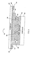
- FIG. 3 shows a second embodiment of the LED 30 constructed in accordance with the present invention, utilizing flip-chip mounting.
- micro-LEDs 32 are formed in an array by etching away semiconductor material of a full LED structure.
- Each micro-LED 32 has an active layer surrounded by two oppositely doped layers.
- the micro-LED arrangement and size is similar to the embodiment described above. However, in this embodiment each of the micro-LEDs has angled side surfaces and their top layer is narrower than its bottom layer.
- the micro-LED array is formed on a first spreader layer 34 that is formed on a substrate 36.
- An insulating layer 38 covers the micro-LEDs and the surface of the first spreader between adjacent micro-LEDS.
- a second spreader layer 42 coats the entire micro-LED array to interconnect the top contacts 40.
- the surface of the second spreader 42 opposite the micro-LEDs is bonded to a reflective metallic layer 48 on a submount 46 by a bonding media.
- a p-contact 44 is included on the metallic layer 48 and current applied to the second contact spreads throughout the second spreader, to the top contacts 40 and to the top layer of the micro-LEDs 32.
- There is a break in the metallic layer 48 and the n-contact 50 is formed on the portion of the metallic layer 48 that is electrically isolated from the portion having the p-contact.
- the finger 49 is bonded between the submount and the first spreader and conducts current from the contact 50 through the metallic layer 48. through the finger and to the first spreader 34. The current then spreads throughout the first spreader and to the bottom layer of the micro-LEDs.
- each micro-LED 32 is AlGaInN based with a p-type top layer.
- Each top contact 40 is preferably Pt, Pt/Au, Pd, Pd/Au, Ni/Au, NiO, or NiO/Au.
- This embodiment provides increased sidewall interaction with the emitted light as a result of the isolated micro-LEDs.
- the portion of the second spreader 42 that is disposed between the micro-LEDs functions as LEEs by reflecting light from the micro-LEDs toward the substrate. This configuration also provides improved heat transfer out of the new LED chip through the submount.
- Figs. 4 and 5 show another embodiment of the new LED 51 that does not have an insulator layer to isolate the first spreader from the second. Instead, micro-LEDs 52 are connected to adjacent micro-LEDs by conductive paths 53 of an interconnected grid 54, wherein the paths have semiconductor material below them. Each opening 55 in the grid 54 is an area where semiconductor material was etched from the LED structure when manufacturing the LED 50. Portions of the structure remain under the grid 54 as micro-LEDs 52 and as semiconductor material under the grid paths 53 between the micro-LEDS.
- the micro-LEDs and the material under the paths comprise an active layer surrounded by two oppositely doped layers, with the entire structure formed on a first spreader layer 56 and a substrate 58.
- a first contact 60 is deposited on the first spreader to apply current to the bottom layer of the micro-LEDs and a second contact 62 is included on the current spreading grid to spread current to the top layer of the micro-LEDs.
- a bias is applied across the contacts 60 and 62, current is applied to the micro-LEDs and the semiconductor material under the conductive paths, all of which emit light. Light escapes from the side surfaces of the micro-LEDs material under the paths, avoiding total internal reflection. This technique is therefore generally applicable to any LED structure on any substrate and is implemented with standard processing techniques.
- the LED 51 is manufactured by first depositing the first spreader layer 56 on the substrate 58, and then forming a continuous LED structure that covers the current spreading layer 56.
- the grid 54 is deposited on the LED structure and portions of the LED structure that are visible in the grid openings are etched away by various methods such as wet chemical etching, Reactive Ion Etching (RIE), Ion Milling, or any other technique used for removing semiconductor material. Portions of the LED structure are also etched to provide an area for contact pads 60, and contact pads 60 and 62 are deposited.
- the grid 54 can be made of any electrically conductive material including but not limited to metals, semi-metals, and semiconductors or combinations thereof.
- the preferred micro-LEDs are GaN-based with each micro-LED's top layer 55 being a p-type AlGaInN or any alloy thereof, and the grid 54 is preferably made of a thin metal such as Ni, Pd, Au, Pt or any combination thereof.
- the dashed line in FIG. 4 illustrates one of the micro-LEDs and the area around the micro-LED where LEEs can be included to further enhance light extraction as more fully described below.
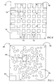
- FIGs. 6 and 7 show two additional embodiments 70 an 80 of the new LED with different micro-LED and grid patterns 72 and 82, although many different patterns can be used.
- Each embodiment has a respective bottom spreading contact 73 and 83.
- the micro-LEDs 74 are interconnected crosses with current spreading to each of the micro-LEDs through the various paths.
- Each path has semiconductor material below it to isolate it from the first spreader layer.
- the grid 72 provides a square array pattern of openings for light interaction.
- the grid 54 has an advantage over grid 72.
- TIR light can reflect down one of the grids numerous conductive paths and reflect within the LED without interacting with a surface of one of the micro-LEDs.
- Optical loss present in the grid or underlying layers will cause some of this TIR light to be absorbed before it can escape out the final edge of the new LED.
- the grid 54 reduces this problem because light emitting from the micro-LEDs will reach a side surface after travelling only a short distance (at most two micro-LED lengths), thereby increasing the light out of the device.
- the micro-LEDs are randomly shaped and have random interconnecting paths. Again, the paths have semiconductor material below them. The random pattern reduces the number of paths for the TIR to travel before it will encounter one of the micro-LEDs in one of the grid openings.
- the dashed lines around the micro-LEOs in FIG. 6 and 7 illustrate the micro-LED 76 anc 36 with LEEs around their perimeters; as more fully described below.
- Opening sizes and distances between openings are preferably between 1 and 30 um, but may be larger or smaller.
- the pattern of the openings may be aperiodic or periodic since the nature of the light interaction with the micro-LED edges does not require either condition.
- the grid openings are between 1 micron and 20 ⁇ m and the micro-LEDs have a width between 1 ⁇ m and 30 ⁇ m .
- All of the previous three embodiments can be integrated with LEEs between micro-LEDs to further increase light emission.
- the LEEs can either be formed on the side surfaces of the micro-LEDs or on the surface of the first spreader layer or the conductive substrate in those embodiments having no first spreader layer.
- FIG. 8 shows several alternative shapes of LEEs that are included as embodiments in this invention, although other shapes can be used and the scope of this invention is not limited to the shapes shown.
- LEEs 82, 84, 86 have curved surfaces while the LEEs 88, 90, 92, 94 have piecewise linear surfaces.
- the LEE may be a randomly roughened layer that acts as a light disperser.
- the LEEs can be formed by standard etching techniques such as wet chemical etching, RIE, or ion milling.
- the LEEs are formed by using a commercially available polymer (such as a UV or e-beam sensitive photoresist) as an ablative etch mask. This polymer is first deposited and patterned with square-like edges. The polymer is heated to a temperature and reflows like glass to give a gradual linear or curved shape to the edges of the polymer. The polymer thickness, pattern shape, heating temperature and heating time will determine the edge shape. The pattern is transferred to the AlGalnN based micro-LEDs with RIE. Linear and curved LEEs are easily fabricated by this method and piecewise linear LEEs can be easily formed by using multiple ablative masks.
- a second technique for forming LEEs is to use a negative polarity UV-exposable photoresist.
- the photoresist is exposed for a particular exposure time and is treated to produce a negative polarity.
- the photoresist is then developed to produce an undercut curved or linear shape in its profile.
- This pattern can then be transferred to the semiconductor material through a dry etching technique.
- the dry etching conditions will also impact the final shape of the lens in the semiconductor material.
- FIGs. 9-15 show embodiments of the new LED with LEEs integrated within the micro-LED array in a variety of ways to enhance light extraction. These embodiments represent a few of the possible ways that the LEEs can be used in accordance with this invention, and the scope of this invention is not limited to the described embodiments.
- FIG. 9 shows a new LED 100 that is similar to the LED 50 in Figs. 4 and 5 , but has LEEs 101, 102, 103 between the micro-LEDs 104.
- the LEEs 101,102,103 allow light that is directed through a micro-LED's side surface to reflect off the LEEs and be re-directed away from the substrate into a package.
- Light rays that reflect off of the interface between the substrate 108 and first spreader layer 106 through TIR can also interact with the LEEs 101,102,103 to escape into the package, providing a higher light output.
- the LEEs depicted in FIG. 8 can be either deposited onto or processed into the new LED. As described above, the depth of the LEEs can also be varied with the preferred depth in the range of 0.5 ⁇ m to 10 ⁇ m
- FIG. 10 shows a new LED 110 similar to the LED 100 in FIG. 9 , but having randomly roughened dispersion LEEs 112 between the micro-LEDs 113.
- the light interaction with the roughened layer allows TIR light to reach the surface within its critical angle and escape before being absorbed.
- the roughened surface is formed by using polystyrene or silica microspheres as an etch mask to transfer micro-scale roughness into the semiconductor.
- the depth and width of the random roughness may be less than 20nm to more that 500nm, with the preferred size being on the order of the wavelength of light generated by the LED.
- FIG 11 shows a new LED 120 that is similar to LED 110 in FIG. 10 , but includes a current- blocking layer within the micro-LED.
- the blocking layer 122 directs current flow underneath the dispersive LEE 124, increasing the chance for light to interact with the LEE and escape.
- the LEEs can be formed directly on the micro-LED side surfaces.
- FIG 12 shows a new LED 130 that is similar to the LEDs ir. FIGs. 9, 10 and 11 , but having various LEEs 131-133 formed directly on each micro-LED's side surfaces.
- the LEEs can be formed using the same methods as described above. Light that travels towards the micro-LED side surfaces is redirected in directions that cause light to escape out one of the surfaces of the substrate 134, through the first spreader layer 135, or through the micro-LEDs 132. Light that is reflected back from the substrate 134 also has an increased chance of escape due to the LEEs on the micro-LED edges.
- FIG 13 shows a new LED 140 where curved LEEs 142 are formed on the side surfaces micro-LEDs 144.
- the curved LEEs 142 provide the additional advantage of focusing the LED light into a more well defined direction.
- the depth and width of the LEEs 142 can be varied with the preferred depth of any one LEE being 0.1 ⁇ m to 50 ⁇ m.
- FIGs. 14 and 15 Two additional embodiments are shown in FIGs. 14 and 15 .
- Figure 14 shows a new LED 150 with a combination of curved LEEs 152 on the side surface if the micro-LEDs 154 and full curved LEEs 156 between the micro-LEDs 154.
- the LEEs work together to enhance light extraction by refracting and reflecting light out of the LED package
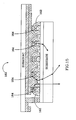
- FIG. 15 shows new LED 160 with curved LEEs 162 on the side surfaces of the micro-LEDs 164, using flip-chip embodiment mounting similar to the embodiment shown in FIG 3 .
- the second spreader 164 is reflective and the substrate 166 is the primary emitting surface.
- the LEEs 162 and the portions of the second spreader 164 work together to enhance light extraction by refracting and reflecting light out of the LED package through the substrate.
- the bottom layers of the micro-LEDs in the array can be in contact.
- the light extraction structures can also be used in many different combinations and can be many different shapes and sizes.
- the LED structure described above can have more than one active layer sandwiched between oppositely doped layers. Therefore, the spirit and scope of the appended claims should not be limited to their preferred embodiments described above.
Landscapes
- Led Devices (AREA)
Applications Claiming Priority (4)
| Application Number | Priority Date | Filing Date | Title |
|---|---|---|---|
| US16881799P | 1999-12-03 | 1999-12-03 | |
| US09/713,576 US6410942B1 (en) | 1999-12-03 | 2000-11-14 | Enhanced light extraction through the use of micro-LED arrays |
| PCT/US2000/032084 WO2001041219A1 (fr) | 1999-12-03 | 2000-11-20 | Reseaux de micro-del a extraction lumineuse accrue |
| EP00980675.3A EP1234334B1 (fr) | 1999-12-03 | 2000-11-20 | Diode électroluminescente à micro-dels pour extraction lumineuse accrue |
Related Parent Applications (5)
| Application Number | Title | Priority Date | Filing Date |
|---|---|---|---|
| WOPCT/US00/32084 Previously-Filed-Application | 2000-11-20 | ||
| PCT/US2000/032084 Previously-Filed-Application WO2001041219A1 (fr) | 1999-12-03 | 2000-11-20 | Reseaux de micro-del a extraction lumineuse accrue |
| EP00980675.3 Division | 2000-11-20 | ||
| EP00980675.3A Division EP1234334B1 (fr) | 1999-12-03 | 2000-11-20 | Diode électroluminescente à micro-dels pour extraction lumineuse accrue |
| EP00980675.3A Division-Into EP1234334B1 (fr) | 1999-12-03 | 2000-11-20 | Diode électroluminescente à micro-dels pour extraction lumineuse accrue |
Publications (3)
| Publication Number | Publication Date |
|---|---|
| EP2325904A2 true EP2325904A2 (fr) | 2011-05-25 |
| EP2325904A3 EP2325904A3 (fr) | 2011-06-01 |
| EP2325904B1 EP2325904B1 (fr) | 2018-08-01 |
Family
ID=26864480
Family Applications (3)
| Application Number | Title | Priority Date | Filing Date |
|---|---|---|---|
| EP10189711.4A Expired - Lifetime EP2325903B1 (fr) | 1999-12-03 | 2000-11-20 | Diode électroluminescente à matrice de micro-DELs pour augmenter l'extraction de lumière |
| EP00980675.3A Expired - Lifetime EP1234334B1 (fr) | 1999-12-03 | 2000-11-20 | Diode électroluminescente à micro-dels pour extraction lumineuse accrue |
| EP10189721.3A Expired - Lifetime EP2325904B1 (fr) | 1999-12-03 | 2000-11-20 | Reseau de micro-diodes electroluminescentes avec extraction de lumiere accrue |
Family Applications Before (2)
| Application Number | Title | Priority Date | Filing Date |
|---|---|---|---|
| EP10189711.4A Expired - Lifetime EP2325903B1 (fr) | 1999-12-03 | 2000-11-20 | Diode électroluminescente à matrice de micro-DELs pour augmenter l'extraction de lumière |
| EP00980675.3A Expired - Lifetime EP1234334B1 (fr) | 1999-12-03 | 2000-11-20 | Diode électroluminescente à micro-dels pour extraction lumineuse accrue |
Country Status (9)
| Country | Link |
|---|---|
| US (1) | US6410942B1 (fr) |
| EP (3) | EP2325903B1 (fr) |
| JP (1) | JP5511114B2 (fr) |
| KR (1) | KR100731673B1 (fr) |
| CN (1) | CN1229871C (fr) |
| AU (1) | AU1790501A (fr) |
| CA (1) | CA2393007C (fr) |
| HK (1) | HK1048707A1 (fr) |
| WO (1) | WO2001041219A1 (fr) |
Families Citing this family (374)
| Publication number | Priority date | Publication date | Assignee | Title |
|---|---|---|---|---|
| HK1048709A1 (zh) * | 1999-12-03 | 2003-04-11 | Cree, Inc. | 透过使用内置及外置光元件提高发光二极管(led)中的抽光效果 |
| US20020017652A1 (en) * | 2000-08-08 | 2002-02-14 | Stefan Illek | Semiconductor chip for optoelectronics |
| US7547921B2 (en) * | 2000-08-08 | 2009-06-16 | Osram Opto Semiconductors Gmbh | Semiconductor chip for optoelectronics |
| JP2002141556A (ja) | 2000-09-12 | 2002-05-17 | Lumileds Lighting Us Llc | 改良された光抽出効果を有する発光ダイオード |
| US7053419B1 (en) | 2000-09-12 | 2006-05-30 | Lumileds Lighting U.S., Llc | Light emitting diodes with improved light extraction efficiency |
| US7064355B2 (en) | 2000-09-12 | 2006-06-20 | Lumileds Lighting U.S., Llc | Light emitting diodes with improved light extraction efficiency |
| JP2002198560A (ja) * | 2000-12-26 | 2002-07-12 | Sharp Corp | 半導体発光素子およびその製造方法 |
| US6791119B2 (en) * | 2001-02-01 | 2004-09-14 | Cree, Inc. | Light emitting diodes including modifications for light extraction |
| JP4724924B2 (ja) * | 2001-02-08 | 2011-07-13 | ソニー株式会社 | 表示装置の製造方法 |
| US6746889B1 (en) * | 2001-03-27 | 2004-06-08 | Emcore Corporation | Optoelectronic device with improved light extraction |
| US6987613B2 (en) | 2001-03-30 | 2006-01-17 | Lumileds Lighting U.S., Llc | Forming an optical element on the surface of a light emitting device for improved light extraction |
| JP2002344011A (ja) * | 2001-05-15 | 2002-11-29 | Sony Corp | 表示素子及びこれを用いた表示装置 |
| US6897704B2 (en) * | 2001-05-25 | 2005-05-24 | Thunder Creative Technologies, Inc. | Electronic isolator |
| TW583348B (en) * | 2001-06-19 | 2004-04-11 | Phoenix Prec Technology Corp | A method for electroplating Ni/Au layer substrate without using electroplating wire |
| JP4055503B2 (ja) | 2001-07-24 | 2008-03-05 | 日亜化学工業株式会社 | 半導体発光素子 |
| US7135711B2 (en) | 2001-08-30 | 2006-11-14 | Osram Opto Semiconductors Gmbh | Electroluminescent body |
| TW523939B (en) * | 2001-11-07 | 2003-03-11 | Nat Univ Chung Hsing | High-efficient light emitting diode and its manufacturing method |
| US6881983B2 (en) * | 2002-02-25 | 2005-04-19 | Kopin Corporation | Efficient light emitting diodes and lasers |
| JP3776824B2 (ja) | 2002-04-05 | 2006-05-17 | 株式会社東芝 | 半導体発光素子およびその製造方法 |
| US20030189215A1 (en) | 2002-04-09 | 2003-10-09 | Jong-Lam Lee | Method of fabricating vertical structure leds |
| JP4585014B2 (ja) * | 2002-04-12 | 2010-11-24 | ソウル セミコンダクター カンパニー リミテッド | 発光装置 |
| EP1536487A4 (fr) * | 2002-05-28 | 2008-02-06 | Matsushita Electric Works Ltd | Element electroluminescent, dispositif electroluminescent et dispositif d'eclairage par emission de surface utilisant ledit element |
| US6841802B2 (en) * | 2002-06-26 | 2005-01-11 | Oriol, Inc. | Thin film light emitting diode |
| US6955985B2 (en) * | 2002-06-28 | 2005-10-18 | Kopin Corporation | Domain epitaxy for thin film growth |
| DE10234977A1 (de) * | 2002-07-31 | 2004-02-12 | Osram Opto Semiconductors Gmbh | Strahlungsemittierendes Dünnschicht-Halbleiterbauelement auf GaN-Basis |
| CN100358163C (zh) * | 2002-08-01 | 2007-12-26 | 日亚化学工业株式会社 | 半导体发光元件及其制造方法、使用此的发光装置 |
| KR20040013998A (ko) * | 2002-08-09 | 2004-02-14 | 엘지전자 주식회사 | 표면 방출형 발광 다이오드의 제조방법 |
| KR100697803B1 (ko) | 2002-08-29 | 2007-03-20 | 시로 사카이 | 복수의 발광 소자를 갖는 발광 장치 |
| JP3956918B2 (ja) | 2002-10-03 | 2007-08-08 | 日亜化学工業株式会社 | 発光ダイオード |
| US7071494B2 (en) * | 2002-12-11 | 2006-07-04 | Lumileds Lighting U.S. Llc | Light emitting device with enhanced optical scattering |
| JP2006512781A (ja) * | 2002-12-30 | 2006-04-13 | オスラム オプト セミコンダクターズ ゲゼルシャフト ミット ベシュレンクテル ハフツング | ボディの表面を粗面化する方法及びオプトエレクトロニクスデバイス |
| US7042020B2 (en) * | 2003-02-14 | 2006-05-09 | Cree, Inc. | Light emitting device incorporating a luminescent material |
| KR100964399B1 (ko) * | 2003-03-08 | 2010-06-17 | 삼성전자주식회사 | 반도체 레이저 다이오드 및 이를 채용한 반도체 레이저다이오드 조립체 |
| US7521854B2 (en) * | 2003-04-15 | 2009-04-21 | Luminus Devices, Inc. | Patterned light emitting devices and extraction efficiencies related to the same |
| US7667238B2 (en) * | 2003-04-15 | 2010-02-23 | Luminus Devices, Inc. | Light emitting devices for liquid crystal displays |
| US7274043B2 (en) * | 2003-04-15 | 2007-09-25 | Luminus Devices, Inc. | Light emitting diode systems |
| US7211831B2 (en) * | 2003-04-15 | 2007-05-01 | Luminus Devices, Inc. | Light emitting device with patterned surfaces |
| US7074631B2 (en) * | 2003-04-15 | 2006-07-11 | Luminus Devices, Inc. | Light emitting device methods |
| US7098589B2 (en) * | 2003-04-15 | 2006-08-29 | Luminus Devices, Inc. | Light emitting devices with high light collimation |
| US7166871B2 (en) * | 2003-04-15 | 2007-01-23 | Luminus Devices, Inc. | Light emitting systems |
| US20040259279A1 (en) * | 2003-04-15 | 2004-12-23 | Erchak Alexei A. | Light emitting device methods |
| US7083993B2 (en) | 2003-04-15 | 2006-08-01 | Luminus Devices, Inc. | Methods of making multi-layer light emitting devices |
| US7084434B2 (en) * | 2003-04-15 | 2006-08-01 | Luminus Devices, Inc. | Uniform color phosphor-coated light-emitting diode |
| US7105861B2 (en) * | 2003-04-15 | 2006-09-12 | Luminus Devices, Inc. | Electronic device contact structures |
| US7262550B2 (en) * | 2003-04-15 | 2007-08-28 | Luminus Devices, Inc. | Light emitting diode utilizing a physical pattern |
| US6831302B2 (en) | 2003-04-15 | 2004-12-14 | Luminus Devices, Inc. | Light emitting devices with improved extraction efficiency |
| EP1620903B1 (fr) * | 2003-04-30 | 2017-08-16 | Cree, Inc. | Blocs de photoemetteurs haute puissance a optiques compactes |
| US7005679B2 (en) | 2003-05-01 | 2006-02-28 | Cree, Inc. | Multiple component solid state white light |
| DE602004028115D1 (de) * | 2003-05-02 | 2010-08-26 | Univ College Cork Nat Univ Ie | Lichtemittierende mesastrukturen mit hohem höhe-zu-breite-verhältnis und quasi-parabolischen seitenwänden und ihre herstellung |
| US6885034B1 (en) | 2003-05-09 | 2005-04-26 | Winston Vaughan Schoenfeld | Light emitting diode having multiple pits |
| US7122841B2 (en) | 2003-06-04 | 2006-10-17 | Kopin Corporation | Bonding pad for gallium nitride-based light-emitting devices |
| US20050000913A1 (en) * | 2003-07-03 | 2005-01-06 | Mark Betterly | Fluid treatment system |
| US7009213B2 (en) | 2003-07-31 | 2006-03-07 | Lumileds Lighting U.S., Llc | Light emitting devices with improved light extraction efficiency |
| EP1652238B1 (fr) * | 2003-08-08 | 2010-10-27 | Kang, Sang-kyu | Micro-diode electroluminescente au nitrure a haute brillance et son procede de fabrication |
| EP1667241B1 (fr) * | 2003-08-19 | 2016-12-07 | Nichia Corporation | Diode électroluminescente semi-conductrice et son procédé de fabrication |
| US7344903B2 (en) * | 2003-09-17 | 2008-03-18 | Luminus Devices, Inc. | Light emitting device processes |
| US7341880B2 (en) * | 2003-09-17 | 2008-03-11 | Luminus Devices, Inc. | Light emitting device processes |
| US7915085B2 (en) * | 2003-09-18 | 2011-03-29 | Cree, Inc. | Molded chip fabrication method |
| US8604497B2 (en) * | 2003-09-26 | 2013-12-10 | Osram Opto Semiconductors Gmbh | Radiation-emitting thin-film semiconductor chip |
| US7704763B2 (en) | 2003-12-09 | 2010-04-27 | The Regents Of The University Of California | Highly efficient group-III nitride based light emitting diodes via fabrication of structures on an N-face surface |
| US7450311B2 (en) * | 2003-12-12 | 2008-11-11 | Luminus Devices, Inc. | Optical display systems and methods |
| JP2005191099A (ja) * | 2003-12-24 | 2005-07-14 | ▲さん▼圓光電股▲ふん▼有限公司 | 発光ダイオード装置 |
| US20050179046A1 (en) * | 2004-02-13 | 2005-08-18 | Kopin Corporation | P-type electrodes in gallium nitride-based light-emitting devices |
| US20050179042A1 (en) * | 2004-02-13 | 2005-08-18 | Kopin Corporation | Monolithic integration and enhanced light extraction in gallium nitride-based light-emitting devices |
| TWM271252U (en) * | 2004-12-14 | 2005-07-21 | Niching Ind Corp | Package structure of light-emitting device |
| JP2005259891A (ja) * | 2004-03-10 | 2005-09-22 | Toyoda Gosei Co Ltd | 発光装置 |
| US7202141B2 (en) * | 2004-03-29 | 2007-04-10 | J.P. Sercel Associates, Inc. | Method of separating layers of material |
| US7419912B2 (en) * | 2004-04-01 | 2008-09-02 | Cree, Inc. | Laser patterning of light emitting devices |
| US7064356B2 (en) * | 2004-04-16 | 2006-06-20 | Gelcore, Llc | Flip chip light emitting diode with micromesas and a conductive mesh |
| US7795623B2 (en) | 2004-06-30 | 2010-09-14 | Cree, Inc. | Light emitting devices having current reducing structures and methods of forming light emitting devices having current reducing structures |
| US7534633B2 (en) * | 2004-07-02 | 2009-05-19 | Cree, Inc. | LED with substrate modifications for enhanced light extraction and method of making same |
| US20090023239A1 (en) * | 2004-07-22 | 2009-01-22 | Luminus Devices, Inc. | Light emitting device processes |
| US20060038188A1 (en) * | 2004-08-20 | 2006-02-23 | Erchak Alexei A | Light emitting diode systems |
| US20060049418A1 (en) * | 2004-09-03 | 2006-03-09 | Tzi-Chi Wen | Epitaxial structure and fabrication method of nitride semiconductor device |
| US8174037B2 (en) * | 2004-09-22 | 2012-05-08 | Cree, Inc. | High efficiency group III nitride LED with lenticular surface |
| US7737459B2 (en) * | 2004-09-22 | 2010-06-15 | Cree, Inc. | High output group III nitride light emitting diodes |
| US8513686B2 (en) * | 2004-09-22 | 2013-08-20 | Cree, Inc. | High output small area group III nitride LEDs |
| US7259402B2 (en) * | 2004-09-22 | 2007-08-21 | Cree, Inc. | High efficiency group III nitride-silicon carbide light emitting diode |
| US7352006B2 (en) * | 2004-09-28 | 2008-04-01 | Goldeneye, Inc. | Light emitting diodes exhibiting both high reflectivity and high light extraction |
| US7329982B2 (en) | 2004-10-29 | 2008-02-12 | 3M Innovative Properties Company | LED package with non-bonded optical element |
| US20060091411A1 (en) | 2004-10-29 | 2006-05-04 | Ouderkirk Andrew J | High brightness LED package |
| US7404756B2 (en) | 2004-10-29 | 2008-07-29 | 3M Innovative Properties Company | Process for manufacturing optical and semiconductor elements |
| US7419839B2 (en) | 2004-11-12 | 2008-09-02 | Philips Lumileds Lighting Company, Llc | Bonding an optical element to a light emitting device |
| US7462502B2 (en) | 2004-11-12 | 2008-12-09 | Philips Lumileds Lighting Company, Llc | Color control by alteration of wavelength converting element |
| JP2006147679A (ja) * | 2004-11-17 | 2006-06-08 | Sony Corp | 集積型発光ダイオード、集積型発光ダイオードの製造方法、発光ダイオードディスプレイおよび発光ダイオード照明装置 |
| US7304363B1 (en) | 2004-11-26 | 2007-12-04 | United States Of America As Represented By The Secretary Of The Army | Interacting current spreader and junction extender to increase the voltage blocked in the off state of a high power semiconductor device |
| US20060124943A1 (en) * | 2004-12-14 | 2006-06-15 | Elite Optoelectronics Inc. | Large-sized light-emitting diodes with improved light extraction efficiency |
| US8288942B2 (en) | 2004-12-28 | 2012-10-16 | Cree, Inc. | High efficacy white LED |
| JP4687109B2 (ja) * | 2005-01-07 | 2011-05-25 | ソニー株式会社 | 集積型発光ダイオードの製造方法 |
| FI118196B (fi) * | 2005-07-01 | 2007-08-15 | Optogan Oy | Puolijohderakenne ja puolijohderakenteen valmistusmenetelmä |
| KR101138974B1 (ko) * | 2005-01-07 | 2012-04-25 | 서울옵토디바이스주식회사 | 발광 소자 및 이의 제조 방법 |
| US20060154393A1 (en) * | 2005-01-11 | 2006-07-13 | Doan Trung T | Systems and methods for removing operating heat from a light emitting diode |
| US20060151801A1 (en) * | 2005-01-11 | 2006-07-13 | Doan Trung T | Light emitting diode with thermo-electric cooler |
| US7524686B2 (en) * | 2005-01-11 | 2009-04-28 | Semileds Corporation | Method of making light emitting diodes (LEDs) with improved light extraction by roughening |
| US7186580B2 (en) * | 2005-01-11 | 2007-03-06 | Semileds Corporation | Light emitting diodes (LEDs) with improved light extraction by roughening |
| US7692207B2 (en) * | 2005-01-21 | 2010-04-06 | Luminus Devices, Inc. | Packaging designs for LEDs |
| US7170100B2 (en) | 2005-01-21 | 2007-01-30 | Luminus Devices, Inc. | Packaging designs for LEDs |
| US7335920B2 (en) * | 2005-01-24 | 2008-02-26 | Cree, Inc. | LED with current confinement structure and surface roughening |
| KR101138944B1 (ko) * | 2005-01-26 | 2012-04-25 | 서울옵토디바이스주식회사 | 직렬 연결된 복수개의 발광셀들을 갖는 발광 소자 및그것을 제조하는 방법 |
| US7535028B2 (en) * | 2005-02-03 | 2009-05-19 | Ac Led Lighting, L.Lc. | Micro-LED based high voltage AC/DC indicator lamp |
| JP2006261659A (ja) * | 2005-02-18 | 2006-09-28 | Sumitomo Chemical Co Ltd | 半導体発光素子の製造方法 |
| US7932111B2 (en) | 2005-02-23 | 2011-04-26 | Cree, Inc. | Substrate removal process for high light extraction LEDs |
| US20060204865A1 (en) * | 2005-03-08 | 2006-09-14 | Luminus Devices, Inc. | Patterned light-emitting devices |
| US20070045640A1 (en) | 2005-08-23 | 2007-03-01 | Erchak Alexei A | Light emitting devices for liquid crystal displays |
| US8163575B2 (en) * | 2005-06-17 | 2012-04-24 | Philips Lumileds Lighting Company Llc | Grown photonic crystals in semiconductor light emitting devices |
| KR100599012B1 (ko) | 2005-06-29 | 2006-07-12 | 서울옵토디바이스주식회사 | 열전도성 기판을 갖는 발광 다이오드 및 그것을 제조하는방법 |
| US20090179211A1 (en) * | 2005-07-14 | 2009-07-16 | Tae-Kyung Yoo | Light emitting device |
| US20070018182A1 (en) * | 2005-07-20 | 2007-01-25 | Goldeneye, Inc. | Light emitting diodes with improved light extraction and reflectivity |
| US8674375B2 (en) * | 2005-07-21 | 2014-03-18 | Cree, Inc. | Roughened high refractive index layer/LED for high light extraction |
| US7348603B2 (en) * | 2005-10-17 | 2008-03-25 | Luminus Devices, Inc. | Anisotropic collimation devices and related methods |
| US7388233B2 (en) * | 2005-10-17 | 2008-06-17 | Luminus Devices, Inc. | Patchwork patterned devices and related methods |
| US7391059B2 (en) | 2005-10-17 | 2008-06-24 | Luminus Devices, Inc. | Isotropic collimation devices and related methods |
| US20070085098A1 (en) * | 2005-10-17 | 2007-04-19 | Luminus Devices, Inc. | Patterned devices and related methods |
| US20080099777A1 (en) * | 2005-10-19 | 2008-05-01 | Luminus Devices, Inc. | Light-emitting devices and related systems |
| KR100779078B1 (ko) * | 2005-12-09 | 2007-11-27 | 한국전자통신연구원 | 빛의 방출 효율을 향상시킬 수 있는 실리콘 발광 소자 및그 제조방법 |
| JP4908837B2 (ja) * | 2005-12-13 | 2012-04-04 | キヤノン株式会社 | 発光素子アレイ及び画像形成装置 |
| EP1969633B1 (fr) | 2005-12-22 | 2018-08-29 | Cree, Inc. | Dispositif d' eclairage |
| WO2007081719A2 (fr) | 2006-01-05 | 2007-07-19 | Illumitex, Inc. | Dispositif optique séparé pour diriger de la lumière depuis une del |
| JP2007214260A (ja) * | 2006-02-08 | 2007-08-23 | Matsushita Electric Ind Co Ltd | 半導体発光素子およびその製造方法 |
| KR20070088145A (ko) * | 2006-02-24 | 2007-08-29 | 엘지전자 주식회사 | 발광 다이오드 및 그 제조방법 |
| US7390117B2 (en) | 2006-05-02 | 2008-06-24 | 3M Innovative Properties Company | LED package with compound converging optical element |
| US7525126B2 (en) | 2006-05-02 | 2009-04-28 | 3M Innovative Properties Company | LED package with converging optical element |
| WO2007139894A2 (fr) | 2006-05-26 | 2007-12-06 | Cree Led Lighting Solutions, Inc. | Dispositif électroluminescent à semi-conducteurs et procédé de fabrication correspondant |
| US8596819B2 (en) | 2006-05-31 | 2013-12-03 | Cree, Inc. | Lighting device and method of lighting |
| KR100759896B1 (ko) * | 2006-06-15 | 2007-09-18 | 삼성전자주식회사 | 적어도 하나의 발광소자가 장착된 백라이트 모듈 및 그제작 방법 |
| US7674639B2 (en) * | 2006-08-14 | 2010-03-09 | Bridgelux, Inc | GaN based LED with etched exposed surface for improved light extraction efficiency and method for making the same |
| WO2008024385A2 (fr) * | 2006-08-23 | 2008-02-28 | Cree Led Lighting Solutions, Inc. | Dispositif d'éclairage et procédé d'éclairage |
| US20100224890A1 (en) * | 2006-09-18 | 2010-09-09 | Cree, Inc. | Light emitting diode chip with electrical insulation element |
| US8087960B2 (en) | 2006-10-02 | 2012-01-03 | Illumitex, Inc. | LED system and method |
| US20090275157A1 (en) * | 2006-10-02 | 2009-11-05 | Illumitex, Inc. | Optical device shaping |
| US20080087875A1 (en) * | 2006-10-11 | 2008-04-17 | Feng-Hsu Fan | Protection for the epitaxial structure of metal devices |
| US9318327B2 (en) | 2006-11-28 | 2016-04-19 | Cree, Inc. | Semiconductor devices having low threading dislocations and improved light extraction and methods of making the same |
| WO2008070604A1 (fr) * | 2006-12-04 | 2008-06-12 | Cree Led Lighting Solutions, Inc. | Dispositif d'éclairage et procédé d'éclairage |
| EP2095011A1 (fr) | 2006-12-04 | 2009-09-02 | Cree Led Lighting Solutions, Inc. | Ensemble éclairage et procédé d'éclairage |
| US8110838B2 (en) * | 2006-12-08 | 2012-02-07 | Luminus Devices, Inc. | Spatial localization of light-generating portions in LEDs |
| CN102683376A (zh) | 2007-01-22 | 2012-09-19 | 科锐公司 | 高压发光体、发光体及照明装置 |
| US9391118B2 (en) * | 2007-01-22 | 2016-07-12 | Cree, Inc. | Fault tolerant light emitters, systems incorporating fault tolerant light emitters and methods of fabricating fault tolerant light emitters |
| US8110425B2 (en) | 2007-03-20 | 2012-02-07 | Luminus Devices, Inc. | Laser liftoff structure and related methods |
| KR100849826B1 (ko) | 2007-03-29 | 2008-07-31 | 삼성전기주식회사 | 발광소자 및 이를 포함하는 패키지 |
| JP5431320B2 (ja) * | 2007-07-17 | 2014-03-05 | クリー インコーポレイテッド | 内部光学機能を備えた光学素子およびその製造方法 |
| US8617997B2 (en) * | 2007-08-21 | 2013-12-31 | Cree, Inc. | Selective wet etching of gold-tin based solder |
| US11114594B2 (en) * | 2007-08-24 | 2021-09-07 | Creeled, Inc. | Light emitting device packages using light scattering particles of different size |
| US8368100B2 (en) * | 2007-11-14 | 2013-02-05 | Cree, Inc. | Semiconductor light emitting diodes having reflective structures and methods of fabricating same |
| US9431589B2 (en) * | 2007-12-14 | 2016-08-30 | Cree, Inc. | Textured encapsulant surface in LED packages |
| DE102008019902A1 (de) * | 2007-12-21 | 2009-06-25 | Osram Opto Semiconductors Gmbh | Optoelektronisches Bauelement und Herstellungsverfahren für ein optoelektronisches Bauelement |
| DE102008003182A1 (de) * | 2008-01-04 | 2009-07-09 | Osram Opto Semiconductors Gmbh | Optoelektronisches Bauelement |
| JP2011512037A (ja) | 2008-02-08 | 2011-04-14 | イルミテックス, インコーポレイテッド | エミッタ層成形のためのシステムおよび方法 |
| JP5094535B2 (ja) * | 2008-05-07 | 2012-12-12 | 富士フイルム株式会社 | 凹部形成方法、凹凸製品の製造方法、発光素子の製造方法および光学素子の製造方法 |
| EP2303039A4 (fr) * | 2008-06-11 | 2011-08-31 | Susanne Gardner | Boissons composées de composants à base de vin |
| US7939839B2 (en) * | 2008-09-11 | 2011-05-10 | Bridgelux, Inc. | Series connected segmented LED |
| US7825427B2 (en) * | 2008-09-12 | 2010-11-02 | Bridgelux, Inc. | Method and apparatus for generating phosphor film with textured surface |
| US9051177B2 (en) * | 2008-10-27 | 2015-06-09 | The United States Of America As Represented By The Secretary Of The Army | Active optical limiting semiconductor device and method with active region transparent to light becoming opaque when not biased |
| TWI375338B (en) * | 2008-11-27 | 2012-10-21 | Epistar Corp | Opto-electronic device |
| TW201034256A (en) | 2008-12-11 | 2010-09-16 | Illumitex Inc | Systems and methods for packaging light-emitting diode devices |
| TWI418060B (zh) * | 2008-12-26 | 2013-12-01 | Lextar Electronics Corp | 發光二極體晶片的製造方法 |
| US7982409B2 (en) * | 2009-02-26 | 2011-07-19 | Bridgelux, Inc. | Light sources utilizing segmented LEDs to compensate for manufacturing variations in the light output of individual segmented LEDs |
| KR101134810B1 (ko) | 2009-03-03 | 2012-04-13 | 엘지이노텍 주식회사 | 발광소자 및 그 제조방법 |
| JP5196403B2 (ja) * | 2009-03-23 | 2013-05-15 | 国立大学法人山口大学 | サファイア基板の製造方法、および半導体装置 |
| US8449128B2 (en) | 2009-08-20 | 2013-05-28 | Illumitex, Inc. | System and method for a lens and phosphor layer |
| US8585253B2 (en) | 2009-08-20 | 2013-11-19 | Illumitex, Inc. | System and method for color mixing lens array |
| KR20110043282A (ko) * | 2009-10-21 | 2011-04-27 | 엘지이노텍 주식회사 | 발광소자 및 그 제조방법 |
| KR101039931B1 (ko) * | 2009-10-21 | 2011-06-09 | 엘지이노텍 주식회사 | 발광 소자 및 그 제조방법 |
| US8783915B2 (en) | 2010-02-11 | 2014-07-22 | Bridgelux, Inc. | Surface-textured encapsulations for use with light emitting diodes |
| US8338317B2 (en) | 2011-04-06 | 2012-12-25 | Infineon Technologies Ag | Method for processing a semiconductor wafer or die, and particle deposition device |
| KR100999733B1 (ko) * | 2010-02-18 | 2010-12-08 | 엘지이노텍 주식회사 | 발광 소자, 발광 소자 제조방법 및 발광 소자 패키지 |
| KR101601624B1 (ko) * | 2010-02-19 | 2016-03-09 | 삼성전자주식회사 | 멀티셀 어레이를 갖는 반도체 발광장치, 발광모듈 및 조명장치 |
| TWI485884B (zh) * | 2010-03-30 | 2015-05-21 | Advanced Optoelectronic Tech | 發光二極體及其製作方法 |
| US8329482B2 (en) | 2010-04-30 | 2012-12-11 | Cree, Inc. | White-emitting LED chips and method for making same |
| KR20110132136A (ko) * | 2010-06-01 | 2011-12-07 | 삼성전자주식회사 | 연결 구조를 이용한 발광소자 및 그 제조 방법 |
| US8193546B2 (en) * | 2010-06-04 | 2012-06-05 | Pinecone Energies, Inc. | Light-emitting-diode array with polymer between light emitting devices |
| KR20180126634A (ko) | 2010-07-26 | 2018-11-27 | 가부시키가이샤 한도오따이 에네루기 켄큐쇼 | 발광 디바이스 및 조명 디바이스 |
| US9070851B2 (en) | 2010-09-24 | 2015-06-30 | Seoul Semiconductor Co., Ltd. | Wafer-level light emitting diode package and method of fabricating the same |
| US9899329B2 (en) | 2010-11-23 | 2018-02-20 | X-Celeprint Limited | Interconnection structures and methods for transfer-printed integrated circuit elements with improved interconnection alignment tolerance |
| JP5589812B2 (ja) | 2010-12-06 | 2014-09-17 | 豊田合成株式会社 | 半導体発光素子 |
| US9166126B2 (en) | 2011-01-31 | 2015-10-20 | Cree, Inc. | Conformally coated light emitting devices and methods for providing the same |
| TWI467805B (zh) * | 2011-03-08 | 2015-01-01 | 光磊科技股份有限公司 | 具寬視角的發光二極體及其製造方法 |
| KR101106139B1 (ko) * | 2011-04-04 | 2012-01-20 | 서울옵토디바이스주식회사 | 확장된 금속 반사층을 갖는 플립 본딩형 발광다이오드 및 그 제조방법 |
| KR101115538B1 (ko) * | 2011-04-04 | 2012-02-28 | 서울옵토디바이스주식회사 | 발광소자와 그 제조방법 |
| US20120261686A1 (en) * | 2011-04-12 | 2012-10-18 | Lu Chi Wei | Light-emitting element and the manufacturing method thereof |
| KR101737981B1 (ko) | 2011-05-17 | 2017-05-22 | 한국전자통신연구원 | 마이크로 어레이 형태의 질화물 발광 소자 및 그 제조 방법 |
| US8934259B2 (en) | 2011-06-08 | 2015-01-13 | Semprius, Inc. | Substrates with transferable chiplets |
| KR101221336B1 (ko) * | 2011-07-12 | 2013-01-21 | 서울옵토디바이스주식회사 | 발광 소자 및 그것을 제조하는 방법 |
| US8957440B2 (en) | 2011-10-04 | 2015-02-17 | Cree, Inc. | Light emitting devices with low packaging factor |
| KR101901589B1 (ko) * | 2011-11-14 | 2018-09-27 | 엘지이노텍 주식회사 | 발광소자 |
| US8426227B1 (en) | 2011-11-18 | 2013-04-23 | LuxVue Technology Corporation | Method of forming a micro light emitting diode array |
| US8573469B2 (en) | 2011-11-18 | 2013-11-05 | LuxVue Technology Corporation | Method of forming a micro LED structure and array of micro LED structures with an electrically insulating layer |
| US8646505B2 (en) | 2011-11-18 | 2014-02-11 | LuxVue Technology Corporation | Micro device transfer head |
| US8349116B1 (en) | 2011-11-18 | 2013-01-08 | LuxVue Technology Corporation | Micro device transfer head heater assembly and method of transferring a micro device |
| KR101337613B1 (ko) * | 2011-12-06 | 2013-12-06 | 서울바이오시스 주식회사 | 발광소자와 그 제조방법 |
| CA2862351A1 (fr) | 2012-02-02 | 2013-08-08 | The Procter & Gamble Company | Stratifie d'emission de lumiere et son procede de fabrication |
| WO2013117760A1 (fr) | 2012-02-10 | 2013-08-15 | University College Cork, National University Of Ireland, Cork | Puce de diode électroluminescente |
| TWI467935B (zh) * | 2012-03-06 | 2015-01-01 | Ind Tech Res Inst | 可見光通訊收發器與系統 |
| GB201215632D0 (en) | 2012-09-03 | 2012-10-17 | Infiniled Ltd | Optical device |
| JP5462333B1 (ja) | 2012-09-21 | 2014-04-02 | 株式会社東芝 | 半導体発光素子及びその製造方法 |
| DE102012109460B4 (de) | 2012-10-04 | 2024-03-07 | OSRAM Opto Semiconductors Gesellschaft mit beschränkter Haftung | Verfahren zur Herstellung eines Leuchtdioden-Displays und Leuchtdioden-Display |
| KR20150084999A (ko) * | 2012-11-15 | 2015-07-22 | 4233999 캐나다 인크. | 마이크로 발광 다이오드를 이용하는 고속 단거리 광 통신을 위한 방법 및 장치 |
| US8558254B1 (en) | 2012-11-29 | 2013-10-15 | Hong Kong Applied Science and Technology Research Institute Company Limited | High reliability high voltage vertical LED arrays |
| US9166114B2 (en) * | 2012-12-11 | 2015-10-20 | LuxVue Technology Corporation | Stabilization structure including sacrificial release layer and staging cavity |
| US9105714B2 (en) * | 2012-12-11 | 2015-08-11 | LuxVue Technology Corporation | Stabilization structure including sacrificial release layer and staging bollards |
| US9306138B2 (en) * | 2013-04-08 | 2016-04-05 | Xiamen Sanan Optoelectronics Technology Co., Ltd. | Light emitting diode packaging structure |
| EP3008553B1 (fr) | 2013-06-12 | 2023-06-07 | Rohinni, Inc. | Rétroéclairage de clavier au moyen de sources de génération de lumière réalisées par dépôt |
| CN104241262B (zh) | 2013-06-14 | 2020-11-06 | 惠州科锐半导体照明有限公司 | 发光装置以及显示装置 |
| DE102013107967B4 (de) * | 2013-07-25 | 2021-05-06 | OSRAM Opto Semiconductors Gesellschaft mit beschränkter Haftung | Optoelektronischer Halbleiterchip, optoelektronisches Bauelement und Verfahren zur Herstellung einer Mehrzahl von optoelektronischen Halbleiterchips |
| JP2014064012A (ja) * | 2013-10-28 | 2014-04-10 | Toshiba Corp | 半導体発光素子及びその製造方法 |
| JP6684541B2 (ja) * | 2014-01-20 | 2020-04-22 | ローム株式会社 | 発光素子 |
| DE102014009677A1 (de) * | 2014-02-19 | 2015-08-20 | Pierre-Alain Cotte | Anzeigevorrichtung mit verbessertem Kontrast |
| US9231153B2 (en) * | 2014-05-30 | 2016-01-05 | Mikro Mesa Technology Co., Ltd. | Micro-light-emitting diode |
| US9105813B1 (en) * | 2014-05-30 | 2015-08-11 | Mikro Mesa Technology Co., Ltd. | Micro-light-emitting diode |
| TWI814461B (zh) | 2014-06-18 | 2023-09-01 | 愛爾蘭商艾克斯展示公司技術有限公司 | 微組裝發光二極體顯示器及照明元件 |
| US9716082B2 (en) | 2014-08-26 | 2017-07-25 | X-Celeprint Limited | Micro assembled hybrid displays and lighting elements |
| US9799261B2 (en) | 2014-09-25 | 2017-10-24 | X-Celeprint Limited | Self-compensating circuit for faulty display pixels |
| US9818725B2 (en) | 2015-06-01 | 2017-11-14 | X-Celeprint Limited | Inorganic-light-emitter display with integrated black matrix |
| US9991163B2 (en) | 2014-09-25 | 2018-06-05 | X-Celeprint Limited | Small-aperture-ratio display with electrical component |
| US9799719B2 (en) | 2014-09-25 | 2017-10-24 | X-Celeprint Limited | Active-matrix touchscreen |
| US9433050B2 (en) * | 2014-10-08 | 2016-08-30 | Mikro Mesa Technology Co., Ltd. | Micro-light-emitting diode |
| US10516084B2 (en) | 2014-10-31 | 2019-12-24 | eLux, Inc. | Encapsulated fluid assembly emissive elements |
| US12119432B2 (en) * | 2014-10-31 | 2024-10-15 | eLux, Inc. | Encapsulated light emitting diodes for selective fluidic assembly |
| GB201420452D0 (en) * | 2014-11-18 | 2014-12-31 | Mled Ltd | Integrated colour led micro-display |
| USD826871S1 (en) | 2014-12-11 | 2018-08-28 | Cree, Inc. | Light emitting diode device |
| KR102347533B1 (ko) * | 2014-12-26 | 2022-01-05 | 삼성디스플레이 주식회사 | 디스플레이 장치 및 그 제조방법 |
| KR102175991B1 (ko) | 2014-12-26 | 2020-11-09 | 삼성디스플레이 주식회사 | 디스플레이 장치 및 그 제조방법 |
| TWI610459B (zh) * | 2015-05-13 | 2018-01-01 | 友達光電股份有限公司 | 微型發光二極體裝置與其製造方法 |
| US9871345B2 (en) | 2015-06-09 | 2018-01-16 | X-Celeprint Limited | Crystalline color-conversion device |
| CN106299095A (zh) * | 2015-06-12 | 2017-01-04 | 映瑞光电科技(上海)有限公司 | 一种高压倒装led芯片及其制作方法 |
| US11061276B2 (en) | 2015-06-18 | 2021-07-13 | X Display Company Technology Limited | Laser array display |
| US10133426B2 (en) | 2015-06-18 | 2018-11-20 | X-Celeprint Limited | Display with micro-LED front light |
| US10255834B2 (en) | 2015-07-23 | 2019-04-09 | X-Celeprint Limited | Parallel redundant chiplet system for controlling display pixels |
| US10380930B2 (en) | 2015-08-24 | 2019-08-13 | X-Celeprint Limited | Heterogeneous light emitter display system |
| KR102393374B1 (ko) | 2015-08-31 | 2022-05-03 | 삼성디스플레이 주식회사 | 표시 장치 및 상기 표시 장치의 제조 방법 |
| KR102424975B1 (ko) * | 2015-08-31 | 2022-07-26 | 삼성디스플레이 주식회사 | 발광 다이오드 구조체 및 디스플레이 장치 |
| USD803472S1 (en) | 2015-09-03 | 2017-11-21 | Svv Technology Innovations, Inc. | Light emitting sheet with surface pattern |
| USD829969S1 (en) | 2015-09-03 | 2018-10-02 | Svv Technology Innovations, Inc. | Light emitting sheet with surface pattern |
| USD799738S1 (en) | 2015-09-03 | 2017-10-10 | Svv Technology Innovations, Inc. | LED lighting sheet with surface pattern |
| USD777972S1 (en) | 2015-09-03 | 2017-01-31 | Svv Technology Innovations, Inc. | Light emitting sheet with surface pattern |
| US10230048B2 (en) | 2015-09-29 | 2019-03-12 | X-Celeprint Limited | OLEDs for micro transfer printing |
| TWI576007B (zh) | 2015-11-23 | 2017-03-21 | 財團法人工業技術研究院 | 發光裝置的驅動方法與發光裝置 |
| US10066819B2 (en) | 2015-12-09 | 2018-09-04 | X-Celeprint Limited | Micro-light-emitting diode backlight system |
| US9742492B2 (en) | 2015-12-30 | 2017-08-22 | Surefire Llc | Systems and methods for ad-hoc networking in an optical narrowcasting system |
| US10629393B2 (en) | 2016-01-15 | 2020-04-21 | Rohinni, LLC | Apparatus and method of backlighting through a cover on the apparatus |
| TWI710061B (zh) | 2016-02-25 | 2020-11-11 | 愛爾蘭商艾克斯展示公司技術有限公司 | 有效率地微轉印微型裝置於大尺寸基板上 |
| US10193025B2 (en) | 2016-02-29 | 2019-01-29 | X-Celeprint Limited | Inorganic LED pixel structure |
| US10153256B2 (en) | 2016-03-03 | 2018-12-11 | X-Celeprint Limited | Micro-transfer printable electronic component |
| US10153257B2 (en) | 2016-03-03 | 2018-12-11 | X-Celeprint Limited | Micro-printed display |
| CN205944139U (zh) | 2016-03-30 | 2017-02-08 | 首尔伟傲世有限公司 | 紫外线发光二极管封装件以及包含此的发光二极管模块 |
| US10199546B2 (en) | 2016-04-05 | 2019-02-05 | X-Celeprint Limited | Color-filter device |
| US10008483B2 (en) | 2016-04-05 | 2018-06-26 | X-Celeprint Limited | Micro-transfer printed LED and color filter structure |
| NL2016716B1 (en) | 2016-05-02 | 2017-11-10 | Nts Systems Dev B V | Exposure system, printing system, method for additive manufacturing, a composition, and the use thereof. |
| US9997501B2 (en) | 2016-06-01 | 2018-06-12 | X-Celeprint Limited | Micro-transfer-printed light-emitting diode device |
| US11137641B2 (en) | 2016-06-10 | 2021-10-05 | X Display Company Technology Limited | LED structure with polarized light emission |
| KR102608419B1 (ko) * | 2016-07-12 | 2023-12-01 | 삼성디스플레이 주식회사 | 표시장치 및 표시장치의 제조방법 |
| DE102016112972A1 (de) * | 2016-07-14 | 2018-01-18 | Osram Opto Semiconductors Gmbh | Optoelektronischer Halbleiterchip |
| US9980341B2 (en) | 2016-09-22 | 2018-05-22 | X-Celeprint Limited | Multi-LED components |
| US10782002B2 (en) | 2016-10-28 | 2020-09-22 | X Display Company Technology Limited | LED optical components |
| US10347168B2 (en) | 2016-11-10 | 2019-07-09 | X-Celeprint Limited | Spatially dithered high-resolution |
| US10395966B2 (en) | 2016-11-15 | 2019-08-27 | X-Celeprint Limited | Micro-transfer-printable flip-chip structures and methods |
| US10600671B2 (en) | 2016-11-15 | 2020-03-24 | X-Celeprint Limited | Micro-transfer-printable flip-chip structures and methods |
| EP3542394B1 (fr) | 2016-11-15 | 2025-09-24 | X Display Company Technology Limited | Structures de puce retournée imprimables par micro-transfert et leurs procédés de fabrication |
| US10193018B2 (en) * | 2016-12-29 | 2019-01-29 | Intel Corporation | Compact low power head-mounted display with light emitting diodes that exhibit a desired beam angle |
| CN109564963B (zh) | 2017-01-26 | 2021-04-16 | 株式会社Lg化学 | 微led和包括其的显示装置 |
| CN106935608B (zh) | 2017-02-27 | 2019-10-25 | 深圳市华星光电技术有限公司 | 微发光二极管阵列基板及显示面板 |
| US11024608B2 (en) | 2017-03-28 | 2021-06-01 | X Display Company Technology Limited | Structures and methods for electrical connection of micro-devices and substrates |
| US9917652B1 (en) | 2017-06-06 | 2018-03-13 | Surefire Llc | Adaptive communications focal plane array |
| DE102017114369A1 (de) * | 2017-06-28 | 2019-01-03 | Osram Opto Semiconductors Gmbh | Optoelektronisches Bauelement |
| KR102418952B1 (ko) | 2017-08-31 | 2022-07-08 | 삼성전자주식회사 | 음성인식 기능을 갖는 가전제품 |
| CN109923683B (zh) * | 2017-09-15 | 2022-04-05 | 厦门市三安光电科技有限公司 | 微型发光二极管及其制作方法 |
| EP3462489B1 (fr) * | 2017-09-29 | 2021-05-26 | Facebook Technologies, LLC | Micro-diode électroluminescente de forme mésa à contact n inférieur |
| US10020422B1 (en) * | 2017-09-29 | 2018-07-10 | Oculus Vr, Llc | Mesa shaped micro light emitting diode with bottom N-contact |
| TWI641778B (zh) | 2017-12-19 | 2018-11-21 | 宏碁股份有限公司 | 微型化發光裝置 |
| US20190198564A1 (en) | 2017-12-20 | 2019-06-27 | Lumileds Llc | Monolithic segmented led array architecture with islanded epitaxial growth |
| US11961875B2 (en) | 2017-12-20 | 2024-04-16 | Lumileds Llc | Monolithic segmented LED array architecture with islanded epitaxial growth |
| KR102428029B1 (ko) | 2017-12-20 | 2022-08-02 | (주)포인트엔지니어링 | 마이크로 led 전사헤드 |
| US11355548B2 (en) | 2017-12-20 | 2022-06-07 | Lumileds Llc | Monolithic segmented LED array architecture |
| US11749790B2 (en) | 2017-12-20 | 2023-09-05 | Lumileds Llc | Segmented LED with embedded transistors |
| US10957820B2 (en) | 2017-12-21 | 2021-03-23 | Lumileds Llc | Monolithic, segmented light emitting diode array |
| US11296262B2 (en) | 2017-12-21 | 2022-04-05 | Lumileds Llc | Monolithic segmented LED array architecture with reduced area phosphor emission surface |
| US20190198720A1 (en) | 2017-12-22 | 2019-06-27 | Lumileds Llc | Particle systems and patterning for monolithic led arrays |
| US10418510B1 (en) | 2017-12-22 | 2019-09-17 | Facebook Technologies, Llc | Mesa shaped micro light emitting diode with electroless plated N-contact |
| US10473439B2 (en) | 2018-01-05 | 2019-11-12 | Aron Surefire, Llc | Gaming systems and methods using optical narrowcasting |
| US10236986B1 (en) | 2018-01-05 | 2019-03-19 | Aron Surefire, Llc | Systems and methods for tiling free space optical transmissions |
| US10250948B1 (en) | 2018-01-05 | 2019-04-02 | Aron Surefire, Llc | Social media with optical narrowcasting |
| KR102536305B1 (ko) | 2018-01-05 | 2023-05-24 | (주)포인트엔지니어링 | 마이크로 led 구조체 및 이의 제조방법 |
| CN110323248B (zh) * | 2018-03-28 | 2021-09-14 | 英属开曼群岛商镎创科技股份有限公司 | 发光二极管显示面板及其制造方法 |
| KR20190114330A (ko) | 2018-03-29 | 2019-10-10 | (주)포인트엔지니어링 | 마이크로 led 전사헤드 |
| KR20190114334A (ko) | 2018-03-29 | 2019-10-10 | (주)포인트엔지니어링 | 마이크로 led 검사 및 리페어 방법 |
| KR20190114333A (ko) | 2018-03-29 | 2019-10-10 | (주)포인트엔지니어링 | 마이크로 led의 검사방법 |
| KR20190114368A (ko) | 2018-03-30 | 2019-10-10 | (주)포인트엔지니어링 | 마이크로 led 반제품 모듈 |
| KR20190114372A (ko) | 2018-03-30 | 2019-10-10 | (주)포인트엔지니어링 | 마이크로 led 전사 시스템 |
| KR102424246B1 (ko) | 2018-03-30 | 2022-07-25 | (주)포인트엔지니어링 | 전사헤드를 구비한 마이크로 led 전사 시스템 |
| KR102481434B1 (ko) | 2018-03-30 | 2022-12-26 | (주)포인트엔지니어링 | 전사헤드 및 이를 이용한 마이크로 led 흡착방법 |
| KR102471585B1 (ko) | 2018-04-06 | 2022-11-28 | (주)포인트엔지니어링 | 마이크로 led 흡착체 및 이를 이용한 마이크로 led 검사시스템 |
| TW201944086A (zh) | 2018-04-06 | 2019-11-16 | 南韓商普因特工程有限公司 | 微發光二極體吸附體 |
| KR102498037B1 (ko) | 2018-04-20 | 2023-02-10 | (주)포인트엔지니어링 | 마이크로 led 흡착체 |
| KR20190117180A (ko) | 2018-04-06 | 2019-10-16 | (주)포인트엔지니어링 | 마이크로 led 흡착체 및 이를 이용한 마이크로 led 검사시스템 |
| KR20190120598A (ko) | 2018-04-16 | 2019-10-24 | (주)포인트엔지니어링 | 마이크로 led 흡착체를 포함하는 마이크로 led 전사 시스템 |
| KR102471583B1 (ko) | 2018-04-16 | 2022-11-28 | (주)포인트엔지니어링 | 마이크로 led 흡착체를 포함하는 마이크로 led 전사 시스템 |
| KR102498109B1 (ko) | 2018-04-20 | 2023-02-09 | (주)포인트엔지니어링 | 마이크로 led 전사 시스템 |
| KR102498112B1 (ko) | 2018-04-27 | 2023-02-09 | (주)포인트엔지니어링 | 마이크로 led 전사 헤드 |
| KR20190124920A (ko) | 2018-04-27 | 2019-11-06 | (주)포인트엔지니어링 | 소자 전사 헤드 |
| KR102527138B1 (ko) | 2018-05-16 | 2023-04-28 | (주)포인트엔지니어링 | 마이크로 led 전사 시스템 |
| KR102517784B1 (ko) | 2018-05-16 | 2023-04-04 | (주)포인트엔지니어링 | 마이크로 led 흡착체 |
| KR102457191B1 (ko) | 2018-05-16 | 2022-10-20 | (주)포인트엔지니어링 | 마이크로 led 전사 시스템 |
| KR20190131311A (ko) | 2018-05-16 | 2019-11-26 | (주)포인트엔지니어링 | 마이크로 led 흡착체 |
| KR102540860B1 (ko) | 2018-05-29 | 2023-06-07 | (주)포인트엔지니어링 | 마이크로 led 전사헤드 및 이를 이용한 마이크로 led 전사 시스템 |
| KR20190135862A (ko) | 2018-05-29 | 2019-12-09 | (주)포인트엔지니어링 | 마이크로 led 전사 시스템 |
| CN110544661A (zh) * | 2018-05-29 | 2019-12-06 | 普因特工程有限公司 | 微led转印头及利用其的微led转印系统 |
| KR102540859B1 (ko) | 2018-05-29 | 2023-06-07 | (주)포인트엔지니어링 | 마이크로 led 전사헤드 및 이를 이용한 마이크로 led 전사 시스템 |
| KR102457193B1 (ko) | 2018-05-29 | 2022-10-20 | (주)포인트엔지니어링 | 마이크로 led 흡착체 |
| KR20190136562A (ko) | 2018-05-31 | 2019-12-10 | (주)포인트엔지니어링 | 마이크로 led 전사헤드 |
| KR102527139B1 (ko) | 2018-06-15 | 2023-04-28 | (주)포인트엔지니어링 | 마이크로 led 전사헤드 및 마이크로 led 전사 스테이지 |
| KR102643764B1 (ko) | 2018-06-27 | 2024-03-06 | (주)포인트엔지니어링 | 마이크로 led 전사헤드 |
| KR102541195B1 (ko) | 2018-06-27 | 2023-06-09 | (주)포인트엔지니어링 | 마이크로 led 전사헤드 |
| CN110648956A (zh) | 2018-06-27 | 2020-01-03 | 普因特工程有限公司 | 微发光二极管转印头 |
| KR20200005234A (ko) | 2018-07-06 | 2020-01-15 | (주)포인트엔지니어링 | 마이크로 led 전사헤드 |
| KR20200005235A (ko) | 2018-07-06 | 2020-01-15 | (주)포인트엔지니어링 | 마이크로 led 전사헤드 |
| KR20200005237A (ko) | 2018-07-06 | 2020-01-15 | (주)포인트엔지니어링 | 마이크로 led 전사 헤드 및 이를 이용한 마이크로 led 전사 시스템 |
| KR20200015082A (ko) | 2018-08-02 | 2020-02-12 | (주)포인트엔지니어링 | 마이크로 led 구조체 및 이의 제조방법 |
| KR20200015071A (ko) | 2018-08-02 | 2020-02-12 | (주)포인트엔지니어링 | 마이크로 led 전사헤드 |
| KR20200015076A (ko) | 2018-08-02 | 2020-02-12 | (주)포인트엔지니어링 | 마이크로 led 전사를 위한 열풍헤드 및 이를 이용한 마이크로led 전사 시스템 |
| KR20200015081A (ko) | 2018-08-02 | 2020-02-12 | (주)포인트엔지니어링 | 마이크로 led 전사헤드 |
| KR20200015073A (ko) | 2018-08-02 | 2020-02-12 | (주)포인트엔지니어링 | 마이크로 led 전사 시스템 |
| EP3836234A4 (fr) | 2018-08-10 | 2022-05-04 | Lin, Hong-Cheng | Dispositif de diode, panneau d'affichage et dispositif d'affichage souple |
| KR20200020208A (ko) | 2018-08-16 | 2020-02-26 | (주)포인트엔지니어링 | 마이크로 led 전사 시스템 |
| KR20200020207A (ko) | 2018-08-16 | 2020-02-26 | (주)포인트엔지니어링 | 마이크로 led 전사헤드 |
| KR20200025079A (ko) | 2018-08-29 | 2020-03-10 | (주)포인트엔지니어링 | 전사헤드 |
| US10811460B2 (en) | 2018-09-27 | 2020-10-20 | Lumileds Holding B.V. | Micrometer scale light emitting diode displays on patterned templates and substrates |
| US11201265B2 (en) | 2018-09-27 | 2021-12-14 | Lumileds Llc | Micro light emitting devices |
| US10923628B2 (en) | 2018-09-27 | 2021-02-16 | Lumileds Llc | Micrometer scale light emitting diode displays on patterned templates and substrates |
| US10964845B2 (en) | 2018-09-27 | 2021-03-30 | Lumileds Llc | Micro light emitting devices |
| KR20200053841A (ko) | 2018-11-09 | 2020-05-19 | (주)포인트엔지니어링 | 마이크로 led 위치 오차 보정 캐리어 및 마이크로 led 전사시스템 |
| KR20200085507A (ko) | 2019-01-07 | 2020-07-15 | (주)포인트엔지니어링 | 마이크로 led 전사헤드 |
| KR20200095909A (ko) | 2019-02-01 | 2020-08-11 | (주)포인트엔지니어링 | 마이크로 led 전사헤드 |
| KR20200099019A (ko) | 2019-02-13 | 2020-08-21 | (주)포인트엔지니어링 | 마이크로 led 흡착체 |
| KR20200129751A (ko) | 2019-05-10 | 2020-11-18 | (주)포인트엔지니어링 | 마이크로 led 흡착체 및 이를 이용한 마이크로 led 디스플레이 제작 방법 및 마이크로 led 디스플레이 |
| KR20200135069A (ko) | 2019-05-24 | 2020-12-02 | (주)포인트엔지니어링 | 마이크로 led 디스플레이 제작 방법 및 이를 이용한 마이크로 led 디스플레이 |
| KR102723703B1 (ko) * | 2019-05-28 | 2024-10-31 | 삼성디스플레이 주식회사 | 표시 장치 및 표시 장치 제조 방법 |
| KR102705311B1 (ko) * | 2019-06-13 | 2024-09-10 | 엘지전자 주식회사 | 마이크로미터 단위 크기의 반도체 발광 소자를 이용하는 발광 장치 및 그 제조 방법 |
| KR102708645B1 (ko) | 2019-07-08 | 2024-09-24 | (주)포인트엔지니어링 | 마이크로 led 그룹 기판 및 이의 제조 방법 및 마이크로 led 디스플레이 패널 및 이의 제조 방법 |
| US11152534B2 (en) | 2019-08-07 | 2021-10-19 | Point Engineering Co., Ltd. | Transfer head and method of manufacturing micro LED display using same |
| KR20210020421A (ko) | 2019-08-14 | 2021-02-24 | (주)포인트엔지니어링 | 마이크로 소자 디스플레이 제조 방법 |
| KR102819268B1 (ko) | 2019-08-14 | 2025-06-11 | (주)포인트엔지니어링 | 마이크로 led 전사헤드 |
| KR20210020433A (ko) | 2019-08-14 | 2021-02-24 | (주)포인트엔지니어링 | 마이크로 led 디스플레이 제작 방법 |
| KR20210025216A (ko) | 2019-08-27 | 2021-03-09 | (주)포인트엔지니어링 | 마이크로 led 리페어 장치 및 이를 이용한 마이크로 led 디스플레이 제조방법 |
| KR20210025217A (ko) | 2019-08-27 | 2021-03-09 | (주)포인트엔지니어링 | 마이크로 led 전사헤드 및 이를 이용한 마이크로 led 디스플레이 제조 방법 |
| CN114902432A (zh) * | 2019-10-28 | 2022-08-12 | 加利福尼亚大学董事会 | 具有原子层沉积钝化侧壁、到顶部电接触体的自对准电介质通孔以及无等离子损坏的顶部接触体的微led台面结构的形成 |
| KR20210063671A (ko) | 2019-11-25 | 2021-06-02 | (주)포인트엔지니어링 | 마이크로 led 디스플레이 제작 방법 |
| TWI895301B (zh) * | 2019-12-03 | 2025-09-01 | 加拿大商弗瑞爾公司 | 高效率微裝置 |
| US11674795B2 (en) | 2019-12-18 | 2023-06-13 | Lumileds Llc | Miniature pattern projector using microLEDs and micro-optics |
| US11404473B2 (en) | 2019-12-23 | 2022-08-02 | Lumileds Llc | III-nitride multi-wavelength LED arrays |
| US11923398B2 (en) | 2019-12-23 | 2024-03-05 | Lumileds Llc | III-nitride multi-wavelength LED arrays |
| KR102168570B1 (ko) | 2020-03-03 | 2020-10-21 | 오재열 | 마이크로 led 전사 기판 |
| US11848402B2 (en) | 2020-03-11 | 2023-12-19 | Lumileds Llc | Light emitting diode devices with multilayer composite film including current spreading layer |
| US11735695B2 (en) | 2020-03-11 | 2023-08-22 | Lumileds Llc | Light emitting diode devices with current spreading layer |
| US11942507B2 (en) | 2020-03-11 | 2024-03-26 | Lumileds Llc | Light emitting diode devices |
| US11569415B2 (en) | 2020-03-11 | 2023-01-31 | Lumileds Llc | Light emitting diode devices with defined hard mask opening |
| KR20220014750A (ko) | 2020-07-29 | 2022-02-07 | (주)포인트엔지니어링 | 미소 소자 이송체 및 이를 이용한 미소 소자 정렬 방법 |
| KR20220021173A (ko) | 2020-08-13 | 2022-02-22 | (주)포인트엔지니어링 | 미소 소자 이송체 및 이를 포함하는 미소 소자 전사 시스템 및 미소 소자가 실장되는 전자 제품의 제조 방법 |
| US11626538B2 (en) | 2020-10-29 | 2023-04-11 | Lumileds Llc | Light emitting diode device with tunable emission |
| US11901491B2 (en) | 2020-10-29 | 2024-02-13 | Lumileds Llc | Light emitting diode devices |
| US12040432B2 (en) | 2020-10-30 | 2024-07-16 | Lumileds Llc | Light emitting diode devices with patterned TCO layer including different thicknesses |
| US11631786B2 (en) | 2020-11-12 | 2023-04-18 | Lumileds Llc | III-nitride multi-wavelength LED arrays with etch stop layer |
| US11705534B2 (en) | 2020-12-01 | 2023-07-18 | Lumileds Llc | Methods of making flip chip micro light emitting diodes |
| US11955583B2 (en) | 2020-12-01 | 2024-04-09 | Lumileds Llc | Flip chip micro light emitting diodes |
| US11600656B2 (en) | 2020-12-14 | 2023-03-07 | Lumileds Llc | Light emitting diode device |
| US12484346B2 (en) | 2021-09-03 | 2025-11-25 | Lumileds Singapore Pte. Ltd. | Light emitting diode devices with bonding and/or ohmic contact-reflective material |
| US12402440B2 (en) | 2021-09-03 | 2025-08-26 | Lumileds Llc | Light emitting diode devices with bonding and/or ohmic contact-reflective material |
| US12419137B2 (en) | 2021-09-10 | 2025-09-16 | Lumileds Llc | Light emitting diodes with segmented anodes by pixel |
| US12433080B2 (en) | 2021-09-29 | 2025-09-30 | Lumileds Singapore Pte. Ltd. | Hybrid CMOS micro-LED display layout |
| US12431478B2 (en) | 2021-09-29 | 2025-09-30 | Lumileds Singapore Pte. Ltd. | Hybrid CMOS micro-LED display layout |
| US12568728B2 (en) | 2021-09-29 | 2026-03-03 | Lumileds Singapore Pte. Ltd. | Hybrid CMOS micro-LED display layout |
| US11935987B2 (en) | 2021-11-03 | 2024-03-19 | Lumileds Llc | Light emitting diode arrays with a light-emitting pixel area |
| US12604572B2 (en) | 2021-11-12 | 2026-04-14 | Lumileds Singapore Pte. Ltd. | Thin-film LED array with low refractive index patterned structures and reflector |
| US12588326B2 (en) | 2021-11-12 | 2026-03-24 | Lumileds Singapore Pte. Ltd. | Composite cathode contact for monolithically integrated micro-LEDs, mini-LEDs and LED arrays |
| US12490570B2 (en) | 2021-11-12 | 2025-12-02 | Lumileds Singapore Pte. Ltd. | Thin-film LED array with low refractive index patterned structures |
| US12300774B2 (en) | 2022-02-25 | 2025-05-13 | Meta Platforms Technologies, Llc | Microdisplay architecture with light extraction efficiency enhancement |
Citations (6)
| Publication number | Priority date | Publication date | Assignee | Title |
|---|---|---|---|---|
| US3954534A (en) | 1974-10-29 | 1976-05-04 | Xerox Corporation | Method of forming light emitting diode array with dome geometry |
| US4946547A (en) | 1989-10-13 | 1990-08-07 | Cree Research, Inc. | Method of preparing silicon carbide surfaces for crystal growth |
| US5200022A (en) | 1990-10-03 | 1993-04-06 | Cree Research, Inc. | Method of improving mechanically prepared substrate surfaces of alpha silicon carbide for deposition of beta silicon carbide thereon and resulting product |
| USRE34861E (en) | 1987-10-26 | 1995-02-14 | North Carolina State University | Sublimation of silicon carbide to produce large, device quality single crystals of silicon carbide |
| US5779924A (en) | 1996-03-22 | 1998-07-14 | Hewlett-Packard Company | Ordered interface texturing for a light emitting device |
| US5793062A (en) | 1995-08-10 | 1998-08-11 | Hewlett-Packard Company | Transparent substrate light emitting diodes with directed light output |
Family Cites Families (29)
| Publication number | Priority date | Publication date | Assignee | Title |
|---|---|---|---|---|
| JPS5310840B2 (fr) * | 1972-05-04 | 1978-04-17 | ||
| JPS50105286A (fr) * | 1974-01-24 | 1975-08-19 | ||
| DE2926803A1 (de) | 1979-07-03 | 1981-02-12 | Licentia Gmbh | Elektrolumineszenz-anordnung |
| FR2531814B1 (fr) * | 1982-08-10 | 1986-04-11 | Thomson Csf | Association monolithique de diodes electroluminescentes et de lentilles |
| JPS62123785A (ja) | 1985-11-22 | 1987-06-05 | Fumio Inaba | 半導体発光装置 |
| JP2579931B2 (ja) | 1987-03-27 | 1997-02-12 | キヤノン株式会社 | 発光表示装置 |
| US5153889A (en) * | 1989-05-31 | 1992-10-06 | Kabushiki Kaisha Toshiba | Semiconductor light emitting device |
| US5309001A (en) | 1991-11-25 | 1994-05-03 | Sharp Kabushiki Kaisha | Light-emitting diode having a surface electrode of a tree-like form |
| JP2786375B2 (ja) * | 1992-06-18 | 1998-08-13 | シャープ株式会社 | 発光ダイオード |
| JP2778405B2 (ja) * | 1993-03-12 | 1998-07-23 | 日亜化学工業株式会社 | 窒化ガリウム系化合物半導体発光素子 |
| JP3312049B2 (ja) * | 1993-03-12 | 2002-08-05 | シャープ株式会社 | 半導体発光装置 |
| JP3452982B2 (ja) * | 1994-08-24 | 2003-10-06 | ローム株式会社 | Ledプリントヘッド、およびledアレイチップ、ならびにそのledアレイチップの製造方法 |
| JPH08139366A (ja) | 1994-11-11 | 1996-05-31 | Ricoh Co Ltd | 発光素子およびアレイ状光源並びにその製造方法および光信号送信装置 |
| US5614734A (en) * | 1995-03-15 | 1997-03-25 | Yale University | High efficency LED structure |
| DE19603444C2 (de) | 1996-01-31 | 2003-04-24 | Siemens Ag | LED-Vorrichtung mit mindestens zwei LEDs |
| US5977566A (en) * | 1996-06-05 | 1999-11-02 | Kabushiki Kaisha Toshiba | Compound semiconductor light emitter |
| EP0856202A2 (fr) | 1996-06-11 | 1998-08-05 | Koninklijke Philips Electronics N.V. | Dispositifs emettant de la lumiere visible, y compris des diodes emettant de la lumiere ultraviolette et des elements fluorescents excitables par les ultraviolets et emettant de la lumiere visible et procede de production de tels dispositifs |
| US5708280A (en) * | 1996-06-21 | 1998-01-13 | Motorola | Integrated electro-optical package and method of fabrication |
| US5955749A (en) * | 1996-12-02 | 1999-09-21 | Massachusetts Institute Of Technology | Light emitting device utilizing a periodic dielectric structure |
| US5898185A (en) | 1997-01-24 | 1999-04-27 | International Business Machines Corporation | Hybrid organic-inorganic semiconductor light emitting diodes |
| JP3752339B2 (ja) * | 1997-02-04 | 2006-03-08 | ローム株式会社 | 半導体発光素子 |
| JP3257455B2 (ja) * | 1997-07-17 | 2002-02-18 | 松下電器産業株式会社 | 発光装置 |
| JP3505374B2 (ja) * | 1997-11-14 | 2004-03-08 | 三洋電機株式会社 | 発光部品 |
| GB2331625B (en) * | 1997-11-19 | 2003-02-26 | Hassan Paddy Abdel Salam | led Lamp |
| WO1999031738A2 (fr) * | 1997-12-16 | 1999-06-24 | Koninklijke Philips Electronics N.V. | Del a canaux, au nitrure a?iii¿ |
| JP3691951B2 (ja) * | 1998-01-14 | 2005-09-07 | 東芝電子エンジニアリング株式会社 | 窒化ガリウム系化合物半導体発光素子 |
| JPH11220168A (ja) * | 1998-02-02 | 1999-08-10 | Toyoda Gosei Co Ltd | 窒化ガリウム系化合物半導体素子及びその製造方法 |
| US6410940B1 (en) * | 2000-06-15 | 2002-06-25 | Kansas State University Research Foundation | Micro-size LED and detector arrays for minidisplay, hyper-bright light emitting diodes, lighting, and UV detector and imaging sensor applications |
| US20020017652A1 (en) * | 2000-08-08 | 2002-02-14 | Stefan Illek | Semiconductor chip for optoelectronics |
-
2000
- 2000-11-14 US US09/713,576 patent/US6410942B1/en not_active Expired - Lifetime
- 2000-11-20 WO PCT/US2000/032084 patent/WO2001041219A1/fr not_active Ceased
- 2000-11-20 KR KR1020027007122A patent/KR100731673B1/ko not_active Expired - Fee Related
- 2000-11-20 HK HK03100708.0A patent/HK1048707A1/zh unknown
- 2000-11-20 EP EP10189711.4A patent/EP2325903B1/fr not_active Expired - Lifetime
- 2000-11-20 JP JP2001542391A patent/JP5511114B2/ja not_active Expired - Lifetime
- 2000-11-20 CA CA2393007A patent/CA2393007C/fr not_active Expired - Lifetime
- 2000-11-20 AU AU17905/01A patent/AU1790501A/en not_active Abandoned
- 2000-11-20 CN CNB008166013A patent/CN1229871C/zh not_active Expired - Lifetime
- 2000-11-20 EP EP00980675.3A patent/EP1234334B1/fr not_active Expired - Lifetime
- 2000-11-20 EP EP10189721.3A patent/EP2325904B1/fr not_active Expired - Lifetime
Patent Citations (6)
| Publication number | Priority date | Publication date | Assignee | Title |
|---|---|---|---|---|
| US3954534A (en) | 1974-10-29 | 1976-05-04 | Xerox Corporation | Method of forming light emitting diode array with dome geometry |
| USRE34861E (en) | 1987-10-26 | 1995-02-14 | North Carolina State University | Sublimation of silicon carbide to produce large, device quality single crystals of silicon carbide |
| US4946547A (en) | 1989-10-13 | 1990-08-07 | Cree Research, Inc. | Method of preparing silicon carbide surfaces for crystal growth |
| US5200022A (en) | 1990-10-03 | 1993-04-06 | Cree Research, Inc. | Method of improving mechanically prepared substrate surfaces of alpha silicon carbide for deposition of beta silicon carbide thereon and resulting product |
| US5793062A (en) | 1995-08-10 | 1998-08-11 | Hewlett-Packard Company | Transparent substrate light emitting diodes with directed light output |
| US5779924A (en) | 1996-03-22 | 1998-07-14 | Hewlett-Packard Company | Ordered interface texturing for a light emitting device |
Non-Patent Citations (4)
| Title |
|---|
| KNOCK ET AL.: "Strongly Directional Emission From AlGaAs/GaAs Light Emitting Diodes", APPLIED PHYSICS LETTER, vol. 57, 1990, pages 2327 - 2329 |
| KRAMES: "High Power Truncated Inverted Pyramid (AlxGa1-x) 0.5In0.5P/GaP Light Emitting Diodes Exhibiting >50% External Qauntum Efficiency", APPLIED PHYSICS LETTERS, 1999, pages 75 |
| SHNITZER ET AL.: "30% External Quantum Efficiency From Surface Textured, Thin Film Light Emitting Diodes", APPLIED PHYSICS LETTERS, vol. 63, 1993, pages 2174 - 2176, XP000404433, DOI: doi:10.1063/1.110575 |
| SHNITZER ET AL.: "Ultrahigh spontaneous emission quantum efficiency, 99.7% internally and 72% externally, from AlGaAs/GaAs/AlGaAs double heterostructures", APPLIED PHYSICS LETTERS, vol. 62, 1993, pages 131 - 133, XP000332227, DOI: doi:10.1063/1.109348 |
Also Published As
| Publication number | Publication date |
|---|---|
| EP1234334A1 (fr) | 2002-08-28 |
| EP2325903B1 (fr) | 2020-01-08 |
| CA2393007A1 (fr) | 2001-06-07 |
| KR20020069357A (ko) | 2002-08-30 |
| CN1402880A (zh) | 2003-03-12 |
| CN1229871C (zh) | 2005-11-30 |
| EP2325903A1 (fr) | 2011-05-25 |
| JP2004505434A (ja) | 2004-02-19 |
| EP2325904B1 (fr) | 2018-08-01 |
| CA2393007C (fr) | 2012-05-29 |
| WO2001041219A1 (fr) | 2001-06-07 |
| EP1234334B1 (fr) | 2019-11-13 |
| JP5511114B2 (ja) | 2014-06-04 |
| EP2325904A3 (fr) | 2011-06-01 |
| HK1048707A1 (zh) | 2003-04-11 |
| KR100731673B1 (ko) | 2007-06-25 |
| AU1790501A (en) | 2001-06-12 |
| US6410942B1 (en) | 2002-06-25 |
Similar Documents
| Publication | Publication Date | Title |
|---|---|---|
| EP2325904B1 (fr) | Reseau de micro-diodes electroluminescentes avec extraction de lumiere accrue | |
| US6657236B1 (en) | Enhanced light extraction in LEDs through the use of internal and external optical elements | |
| US8008678B2 (en) | Light-emitting diode with increased light extraction | |
| US20090050905A1 (en) | Highly Efficient Light-Emitting Diode | |
| WO2007015844A2 (fr) | Diodes électroluminescentes à extraction de lumière et réflectivité améliorées | |
| US7915621B2 (en) | Inverted LED structure with improved light extraction | |
| KR100647814B1 (ko) | 고휘도 발광 다이오드 소자 |
Legal Events
| Date | Code | Title | Description |
|---|---|---|---|
| PUAI | Public reference made under article 153(3) epc to a published international application that has entered the european phase |
Free format text: ORIGINAL CODE: 0009012 |
|
| PUAL | Search report despatched |
Free format text: ORIGINAL CODE: 0009013 |
|
| AC | Divisional application: reference to earlier application |
Ref document number: 1234334 Country of ref document: EP Kind code of ref document: P |
|
| AK | Designated contracting states |
Kind code of ref document: A2 Designated state(s): AT BE CH CY DE DK ES FI FR GB GR IE IT LI LU MC NL PT SE TR |
|
| AK | Designated contracting states |
Kind code of ref document: A3 Designated state(s): AT BE CH CY DE DK ES FI FR GB GR IE IT LI LU MC NL PT SE TR |
|
| 17P | Request for examination filed |
Effective date: 20111201 |
|
| 17Q | First examination report despatched |
Effective date: 20160726 |
|
| STAA | Information on the status of an ep patent application or granted ep patent |
Free format text: STATUS: EXAMINATION IS IN PROGRESS |
|
| GRAP | Despatch of communication of intention to grant a patent |
Free format text: ORIGINAL CODE: EPIDOSNIGR1 |
|
| STAA | Information on the status of an ep patent application or granted ep patent |
Free format text: STATUS: GRANT OF PATENT IS INTENDED |
|
| RIC1 | Information provided on ipc code assigned before grant |
Ipc: H01L 33/38 20100101ALN20180102BHEP Ipc: H01L 33/08 20100101AFI20180102BHEP Ipc: H01L 33/42 20100101ALN20180102BHEP Ipc: H01L 33/22 20100101ALN20180102BHEP Ipc: H01L 33/20 20100101ALN20180102BHEP |
|
| RIC1 | Information provided on ipc code assigned before grant |
Ipc: H01L 33/42 20100101ALN20180111BHEP Ipc: H01L 33/20 20100101ALN20180111BHEP Ipc: H01L 33/38 20100101ALN20180111BHEP Ipc: H01L 33/08 20100101AFI20180111BHEP Ipc: H01L 33/22 20100101ALN20180111BHEP |
|
| RIC1 | Information provided on ipc code assigned before grant |
Ipc: H01L 33/42 20100101ALN20180112BHEP Ipc: H01L 33/08 20100101AFI20180112BHEP Ipc: H01L 33/22 20100101ALN20180112BHEP Ipc: H01L 33/38 20100101ALN20180112BHEP Ipc: H01L 33/20 20100101ALN20180112BHEP |
|
| INTG | Intention to grant announced |
Effective date: 20180129 |
|
| GRAS | Grant fee paid |
Free format text: ORIGINAL CODE: EPIDOSNIGR3 |
|
| GRAJ | Information related to disapproval of communication of intention to grant by the applicant or resumption of examination proceedings by the epo deleted |
Free format text: ORIGINAL CODE: EPIDOSDIGR1 |
|
| GRAL | Information related to payment of fee for publishing/printing deleted |
Free format text: ORIGINAL CODE: EPIDOSDIGR3 |
|
| STAA | Information on the status of an ep patent application or granted ep patent |
Free format text: STATUS: EXAMINATION IS IN PROGRESS |
|
| GRAR | Information related to intention to grant a patent recorded |
Free format text: ORIGINAL CODE: EPIDOSNIGR71 |
|
| STAA | Information on the status of an ep patent application or granted ep patent |
Free format text: STATUS: GRANT OF PATENT IS INTENDED |
|
| GRAA | (expected) grant |
Free format text: ORIGINAL CODE: 0009210 |
|
| STAA | Information on the status of an ep patent application or granted ep patent |
Free format text: STATUS: THE PATENT HAS BEEN GRANTED |
|
| INTC | Intention to grant announced (deleted) | ||
| RIC1 | Information provided on ipc code assigned before grant |
Ipc: H01L 33/08 20100101AFI20180619BHEP Ipc: H01L 33/42 20100101ALN20180619BHEP Ipc: H01L 33/20 20100101ALN20180619BHEP Ipc: H01L 33/22 20100101ALN20180619BHEP Ipc: H01L 33/38 20100101ALN20180619BHEP |
|
| AC | Divisional application: reference to earlier application |
Ref document number: 1234334 Country of ref document: EP Kind code of ref document: P |
|
| AK | Designated contracting states |
Kind code of ref document: B1 Designated state(s): AT BE CH CY DE DK ES FI FR GB GR IE IT LI LU MC NL PT SE TR |
|
| INTG | Intention to grant announced |
Effective date: 20180625 |
|
| REG | Reference to a national code |
Ref country code: GB Ref legal event code: FG4D |
|
| REG | Reference to a national code |
Ref country code: CH Ref legal event code: EP Ref country code: AT Ref legal event code: REF Ref document number: 1025346 Country of ref document: AT Kind code of ref document: T Effective date: 20180815 |
|
| REG | Reference to a national code |
Ref country code: IE Ref legal event code: FG4D |
|
| REG | Reference to a national code |
Ref country code: DE Ref legal event code: R096 Ref document number: 60049843 Country of ref document: DE |
|
| REG | Reference to a national code |
Ref country code: NL Ref legal event code: MP Effective date: 20180801 |
|
| REG | Reference to a national code |
Ref country code: AT Ref legal event code: MK05 Ref document number: 1025346 Country of ref document: AT Kind code of ref document: T Effective date: 20180801 |
|
| PG25 | Lapsed in a contracting state [announced via postgrant information from national office to epo] |
Ref country code: NL Free format text: LAPSE BECAUSE OF FAILURE TO SUBMIT A TRANSLATION OF THE DESCRIPTION OR TO PAY THE FEE WITHIN THE PRESCRIBED TIME-LIMIT Effective date: 20180801 Ref country code: GR Free format text: LAPSE BECAUSE OF FAILURE TO SUBMIT A TRANSLATION OF THE DESCRIPTION OR TO PAY THE FEE WITHIN THE PRESCRIBED TIME-LIMIT Effective date: 20181102 Ref country code: FI Free format text: LAPSE BECAUSE OF FAILURE TO SUBMIT A TRANSLATION OF THE DESCRIPTION OR TO PAY THE FEE WITHIN THE PRESCRIBED TIME-LIMIT Effective date: 20180801 Ref country code: SE Free format text: LAPSE BECAUSE OF FAILURE TO SUBMIT A TRANSLATION OF THE DESCRIPTION OR TO PAY THE FEE WITHIN THE PRESCRIBED TIME-LIMIT Effective date: 20180801 Ref country code: AT Free format text: LAPSE BECAUSE OF FAILURE TO SUBMIT A TRANSLATION OF THE DESCRIPTION OR TO PAY THE FEE WITHIN THE PRESCRIBED TIME-LIMIT Effective date: 20180801 |
|
| PG25 | Lapsed in a contracting state [announced via postgrant information from national office to epo] |
Ref country code: ES Free format text: LAPSE BECAUSE OF FAILURE TO SUBMIT A TRANSLATION OF THE DESCRIPTION OR TO PAY THE FEE WITHIN THE PRESCRIBED TIME-LIMIT Effective date: 20180801 |
|
| PG25 | Lapsed in a contracting state [announced via postgrant information from national office to epo] |
Ref country code: IT Free format text: LAPSE BECAUSE OF FAILURE TO SUBMIT A TRANSLATION OF THE DESCRIPTION OR TO PAY THE FEE WITHIN THE PRESCRIBED TIME-LIMIT Effective date: 20180801 |
|
| REG | Reference to a national code |
Ref country code: DE Ref legal event code: R097 Ref document number: 60049843 Country of ref document: DE |
|
| PG25 | Lapsed in a contracting state [announced via postgrant information from national office to epo] |
Ref country code: DK Free format text: LAPSE BECAUSE OF FAILURE TO SUBMIT A TRANSLATION OF THE DESCRIPTION OR TO PAY THE FEE WITHIN THE PRESCRIBED TIME-LIMIT Effective date: 20180801 |
|
| PLBE | No opposition filed within time limit |
Free format text: ORIGINAL CODE: 0009261 |
|
| STAA | Information on the status of an ep patent application or granted ep patent |
Free format text: STATUS: NO OPPOSITION FILED WITHIN TIME LIMIT |
|
| REG | Reference to a national code |
Ref country code: CH Ref legal event code: PL |
|
| 26N | No opposition filed |
Effective date: 20190503 |
|
| GBPC | Gb: european patent ceased through non-payment of renewal fee |
Effective date: 20181120 |
|
| PG25 | Lapsed in a contracting state [announced via postgrant information from national office to epo] |
Ref country code: MC Free format text: LAPSE BECAUSE OF FAILURE TO SUBMIT A TRANSLATION OF THE DESCRIPTION OR TO PAY THE FEE WITHIN THE PRESCRIBED TIME-LIMIT Effective date: 20180801 Ref country code: LU Free format text: LAPSE BECAUSE OF NON-PAYMENT OF DUE FEES Effective date: 20181120 |
|
| REG | Reference to a national code |
Ref country code: BE Ref legal event code: MM Effective date: 20181130 |
|
| REG | Reference to a national code |
Ref country code: IE Ref legal event code: MM4A |
|
| PG25 | Lapsed in a contracting state [announced via postgrant information from national office to epo] |
Ref country code: CH Free format text: LAPSE BECAUSE OF NON-PAYMENT OF DUE FEES Effective date: 20181130 Ref country code: LI Free format text: LAPSE BECAUSE OF NON-PAYMENT OF DUE FEES Effective date: 20181130 |
|
| PG25 | Lapsed in a contracting state [announced via postgrant information from national office to epo] |
Ref country code: FR Free format text: LAPSE BECAUSE OF NON-PAYMENT OF DUE FEES Effective date: 20181130 Ref country code: IE Free format text: LAPSE BECAUSE OF NON-PAYMENT OF DUE FEES Effective date: 20181120 |
|
| PG25 | Lapsed in a contracting state [announced via postgrant information from national office to epo] |
Ref country code: BE Free format text: LAPSE BECAUSE OF NON-PAYMENT OF DUE FEES Effective date: 20181130 |
|
| PG25 | Lapsed in a contracting state [announced via postgrant information from national office to epo] |
Ref country code: GB Free format text: LAPSE BECAUSE OF NON-PAYMENT OF DUE FEES Effective date: 20181120 |
|
| PGFP | Annual fee paid to national office [announced via postgrant information from national office to epo] |
Ref country code: DE Payment date: 20191127 Year of fee payment: 20 |
|
| PG25 | Lapsed in a contracting state [announced via postgrant information from national office to epo] |
Ref country code: TR Free format text: LAPSE BECAUSE OF FAILURE TO SUBMIT A TRANSLATION OF THE DESCRIPTION OR TO PAY THE FEE WITHIN THE PRESCRIBED TIME-LIMIT Effective date: 20180801 |
|
| PG25 | Lapsed in a contracting state [announced via postgrant information from national office to epo] |
Ref country code: PT Free format text: LAPSE BECAUSE OF FAILURE TO SUBMIT A TRANSLATION OF THE DESCRIPTION OR TO PAY THE FEE WITHIN THE PRESCRIBED TIME-LIMIT Effective date: 20180801 |
|
| PG25 | Lapsed in a contracting state [announced via postgrant information from national office to epo] |
Ref country code: CY Free format text: LAPSE BECAUSE OF FAILURE TO SUBMIT A TRANSLATION OF THE DESCRIPTION OR TO PAY THE FEE WITHIN THE PRESCRIBED TIME-LIMIT Effective date: 20180801 |
|
| REG | Reference to a national code |
Ref country code: DE Ref legal event code: R071 Ref document number: 60049843 Country of ref document: DE |