EP2330738A1 - MEMS-Resonator mit Transistor und einen solchen Resonator umfassender Oszillator - Google Patents
MEMS-Resonator mit Transistor und einen solchen Resonator umfassender Oszillator Download PDFInfo
- Publication number
- EP2330738A1 EP2330738A1 EP09177918A EP09177918A EP2330738A1 EP 2330738 A1 EP2330738 A1 EP 2330738A1 EP 09177918 A EP09177918 A EP 09177918A EP 09177918 A EP09177918 A EP 09177918A EP 2330738 A1 EP2330738 A1 EP 2330738A1
- Authority
- EP
- European Patent Office
- Prior art keywords
- transistor
- piezoelectric material
- resonator
- vibrating structure
- channel
- Prior art date
- Legal status (The legal status is an assumption and is not a legal conclusion. Google has not performed a legal analysis and makes no representation as to the accuracy of the status listed.)
- Withdrawn
Links
- 239000000463 material Substances 0.000 claims abstract description 49
- 230000008878 coupling Effects 0.000 claims abstract description 9
- 238000010168 coupling process Methods 0.000 claims abstract description 9
- 238000005859 coupling reaction Methods 0.000 claims abstract description 9
- 239000000758 substrate Substances 0.000 claims description 17
- 230000005284 excitation Effects 0.000 claims description 9
- 239000004065 semiconductor Substances 0.000 claims description 6
- 230000004044 response Effects 0.000 claims description 3
- XUIMIQQOPSSXEZ-UHFFFAOYSA-N Silicon Chemical compound [Si] XUIMIQQOPSSXEZ-UHFFFAOYSA-N 0.000 description 25
- 229910052710 silicon Inorganic materials 0.000 description 25
- 239000010703 silicon Substances 0.000 description 25
- VYPSYNLAJGMNEJ-UHFFFAOYSA-N Silicium dioxide Chemical compound O=[Si]=O VYPSYNLAJGMNEJ-UHFFFAOYSA-N 0.000 description 21
- 230000000694 effects Effects 0.000 description 9
- 235000012239 silicon dioxide Nutrition 0.000 description 9
- 239000000377 silicon dioxide Substances 0.000 description 9
- 230000010287 polarization Effects 0.000 description 8
- 230000005684 electric field Effects 0.000 description 7
- 238000005530 etching Methods 0.000 description 5
- 230000005669 field effect Effects 0.000 description 4
- 238000004519 manufacturing process Methods 0.000 description 4
- 230000008901 benefit Effects 0.000 description 3
- 239000002800 charge carrier Substances 0.000 description 3
- 125000004122 cyclic group Chemical group 0.000 description 3
- 238000010586 diagram Methods 0.000 description 3
- 239000003989 dielectric material Substances 0.000 description 3
- 229910052814 silicon oxide Inorganic materials 0.000 description 3
- 230000008859 change Effects 0.000 description 2
- 239000012212 insulator Substances 0.000 description 2
- 238000001465 metallisation Methods 0.000 description 2
- 239000011347 resin Substances 0.000 description 2
- 229920005989 resin Polymers 0.000 description 2
- 229910004298 SiO 2 Inorganic materials 0.000 description 1
- 230000009471 action Effects 0.000 description 1
- 238000005452 bending Methods 0.000 description 1
- 230000006835 compression Effects 0.000 description 1
- 238000007906 compression Methods 0.000 description 1
- 239000004020 conductor Substances 0.000 description 1
- 238000010276 construction Methods 0.000 description 1
- 238000001514 detection method Methods 0.000 description 1
- 238000006073 displacement reaction Methods 0.000 description 1
- 230000005484 gravity Effects 0.000 description 1
- 238000000034 method Methods 0.000 description 1
- 230000004048 modification Effects 0.000 description 1
- 238000012986 modification Methods 0.000 description 1
- 230000003647 oxidation Effects 0.000 description 1
- 238000007254 oxidation reaction Methods 0.000 description 1
- 229920002120 photoresistant polymer Polymers 0.000 description 1
Images


Classifications
-
- H—ELECTRICITY
- H03—ELECTRONIC CIRCUITRY
- H03H—IMPEDANCE NETWORKS, e.g. RESONANT CIRCUITS; RESONATORS
- H03H9/00—Networks comprising electromechanical or electro-acoustic elements; Electromechanical resonators
- H03H9/02—Details
- H03H9/02244—Details of microelectro-mechanical resonators
- H03H9/02259—Driving or detection means
-
- H—ELECTRICITY
- H03—ELECTRONIC CIRCUITRY
- H03H—IMPEDANCE NETWORKS, e.g. RESONANT CIRCUITS; RESONATORS
- H03H9/00—Networks comprising electromechanical or electro-acoustic elements; Electromechanical resonators
- H03H9/24—Constructional features of resonators of material which is not piezoelectric, electrostrictive, or magnetostrictive
- H03H9/2405—Constructional features of resonators of material which is not piezoelectric, electrostrictive, or magnetostrictive of microelectro-mechanical resonators
- H03H9/2426—Constructional features of resonators of material which is not piezoelectric, electrostrictive, or magnetostrictive of microelectro-mechanical resonators in combination with other electronic elements
-
- H—ELECTRICITY
- H03—ELECTRONIC CIRCUITRY
- H03H—IMPEDANCE NETWORKS, e.g. RESONANT CIRCUITS; RESONATORS
- H03H9/00—Networks comprising electromechanical or electro-acoustic elements; Electromechanical resonators
- H03H9/24—Constructional features of resonators of material which is not piezoelectric, electrostrictive, or magnetostrictive
- H03H9/2405—Constructional features of resonators of material which is not piezoelectric, electrostrictive, or magnetostrictive of microelectro-mechanical resonators
- H03H9/2447—Beam resonators
-
- H—ELECTRICITY
- H03—ELECTRONIC CIRCUITRY
- H03H—IMPEDANCE NETWORKS, e.g. RESONANT CIRCUITS; RESONATORS
- H03H9/00—Networks comprising electromechanical or electro-acoustic elements; Electromechanical resonators
- H03H9/24—Constructional features of resonators of material which is not piezoelectric, electrostrictive, or magnetostrictive
- H03H9/2405—Constructional features of resonators of material which is not piezoelectric, electrostrictive, or magnetostrictive of microelectro-mechanical resonators
- H03H9/2468—Tuning fork resonators
- H03H9/2473—Double-Ended Tuning Fork [DETF] resonators
-
- H—ELECTRICITY
- H03—ELECTRONIC CIRCUITRY
- H03H—IMPEDANCE NETWORKS, e.g. RESONANT CIRCUITS; RESONATORS
- H03H9/00—Networks comprising electromechanical or electro-acoustic elements; Electromechanical resonators
- H03H9/02—Details
- H03H9/02244—Details of microelectro-mechanical resonators
- H03H2009/02283—Vibrating means
- H03H2009/02291—Beams
- H03H2009/02314—Beams forming part of a transistor structure
Definitions
- the present invention relates to transistor MEMS resonators and MEMS oscillators comprising such transistor MEMS resonators.
- the present invention relates more particularly to oscillators comprising a resonant gate transistor, and in particular such oscillators used as a time base.
- Oscillators that use the resonance of an electromechanical resonator to produce a signal of a determined frequency are most often formed of an integrated oscillating circuit, and a piezoelectric coupling resonator which is not itself integrated with the circuit. It will be understood that this construction undesirably increases the size and cost of such devices. A number of solutions have therefore been proposed to provide resonator oscillators that are fully integrated.
- the free end of the beam moves opposite the FET transistor so as to allow vibrations of the beam to control the transistor.
- the beam is biased with a constant voltage relative to the substrate in which the transistor is formed.
- the bias voltage must be high enough that the electric field emanating from the end of the beam influences the conductivity of the field effect transistor.
- the transistor resonator whose operating principle has just been described, has certain disadvantages.
- the bias voltage of the flexible beam must therefore be relatively high; see even higher than the maximum voltage supported by the usual integrated circuits.
- the electromechanical coupling is not optimal, the dynamic resistance (in English "motional resistance") of the resonator is increased.
- An object of the present invention is therefore to provide a MEMS oscillator comprising a resonant gate transistor which has an electromechanical coupling improved independently of the number of transistors and which also has a reduced power consumption.
- the figure 5 of the patent document US 4,873,871 illustrates an accelerometer operating through a mechanical gate transistor (MFET).
- the figure 1 annexed reproduces the figure 5 of this previous document.
- the MFET (referenced 10 ') comprises a substrate 12' and a gate 52.
- the substrate 12 ' comprises a drain 20', a source 22 ', an oxide layer 24' and a plurality of connectors 46 '.
- the substrate 12 'further comprises a zone 44' located between the source and the drain and in which a concentration or a depletion of charge carriers is likely to occur.
- the gate 52 comprises a piezoelectric material 54 as well as a seismic mass 56.
- the piezoelectric material 54 is compressed and is stretched, which has the effect of polarizing the piezoelectric material 54.
- the electric field associated with this polarization varies the concentration of charge carriers in the zone 44 '.
- the piezoelectric material 54 is compressed, electrons are attracted to the surface of the zone 44 'giving rise to a channel through which an electric current can flow between the drain 20' and the source 22 '. Since the electric field generated by the compression of the piezoelectric material is sufficient to change the concentration of charge carriers in the area 44 ', the gate 52 need not be connected to an external voltage source. It will be understood that the transistor described in this document prior art is designed to perform the function of electromechanical transducer and that it is absolutely not a resonant gate transistor.
- An object of the present invention is to overcome the aforementioned drawbacks of the prior art.
- the present invention achieves this goal by providing a transistor MEMS resonator according to claim 1.
- the box comprising the source region, the drain region and the channel connecting the source region and the drain region is integrated in the fixed structure.
- the microstructure of a piezoelectric material is integral with the vibrating structure and separated from the channel by a space.
- the microstructure of a piezoelectric material is integral with both the vibrating structure and the fixed structure.
- the box is integrated in the vibrating structure.
- the microstructure of a piezoelectric material is integral with both the vibrating structure and the fixed structure.
- the present invention also relates to a MEMS oscillator according to claim 11.
- the MEMS oscillator according to the present invention is made around a transistor resonator according to the present invention.
- An advantage associated with the use of the transistor resonator according to the present invention is that the low dynamic resistance of the resonator makes it possible to produce oscillators having a low power consumption.
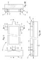
- FIGS. 2, 3A, 3B and 4 illustrate a MEMS oscillator which corresponds to a first embodiment of the present invention. Some components of the oscillator that do not directly relate to the present invention have been omitted so as not to overload the figures.
- the MEMS oscillator of the present example is based on a transistor resonator according to the invention.
- the resonator 100 is entirely produced by etching in a wafer of crystalline or amorphous material, such as silicon.
- a feature of this first embodiment is that the resonator and its transistor are formed in a same plane parallel to the wafer.
- the wafer is of the Silicon On Insulator (SOI) type and comprises a thick silicon substrate 102, an insulating silicon oxide intermediate layer 104, and a silicon top layer 106 in which the resonator is etched.
- SOI Silicon On Insulator
- the resonator of the present example is mainly formed of a resonant frame 110 supported at both ends by supports 112 and 114.
- the support 114 is formed of a silicon dioxide foot surmounted by a silicon arm which comes from the material with the resonant frame 110.
- the support 112 also comprises a foot of silicon dioxide.
- the support 112 is not in direct contact with the frame 110.
- microstructure 126 of a piezoelectric material and an insulating oxide layer 124 are interposed between the support 112 and frame 110 (in this example, microstructure 126 may simply consist of a piezoelectric material thickness).
- the silicon top portion of the support 114 constitutes a p-type semiconductor box for a transistor.
- a conduction element of the transistor consisting of a source region 108, a drain region 109, and an n-doped region (unreferenced) forming a channel for connecting the source region and the drain region is formed in the caisson.
- the insulating oxide layer 124 covers the channel region of the conduction element, and the thickness of piezoelectric material 126 is interposed between the oxide layer 124 and the frame 110.
- the horizontal stack formed by the oxide layer 124 and the piezoelectric material thickness 126 constitutes what is called a "gate stack" (or “gate stack”). According to variants of the invention, the structure of the gate stack may be more complex than that just described.
- the gate stack comprises a gap, that is to say an empty space separating two successive layers of the stack.
- the silicon forming the support 112 has received a p-type doping, and the source 108 and the drain 109 are regions which have subsequently been n-doped.
- the invention is obviously not limited to this variant.
- the resonator substantially in the form of a rectangular frame 110 held in place by its two small sides which are connected to the supports 112 and 114. The long sides of the frame are free to deform. Comparing the figure 2 with the figure 4 which represents the same resonator, one can realize that the frame 110 has a very elongated shape, and that it has been amputated of its central portion on the Figures 2 and 3A . From a functional point of view, the resonator of the figure 2 can be likened to a tuning fork resonator which would be closed at both ends or, better still, a pair of tuning forks placed end to end and whose arms would join.
- the figure 4 illustrates the deformations undergone by the frame 110 in a particular vibration mode. It will be understood that in the vibration mode shown, the two arms of the resonator are always symmetrical, which has the advantage of avoiding any displacement of the center of gravity of the structure transversely to its longitudinal axis. It will be understood, however, that the present invention is not limited to a particular vibration mode. In addition, the present invention is not limited to the particular type of resonator described in this example.
- the resonant frame 110 is also supported on two structures 116, 118.
- the two structures 116, 118 are each formed of a foot silicon dioxide and a silicon arm.
- the arms of the supports 116, 118 are each connected to one of the long sides of the frame 110.
- a thickness of piezoelectric material 122 is interposed between each of the arms and the corresponding side of the frame 110.
- the structures 116, 118 are provided to vibrate the two long sides of the frame 110 through the piezoelectric effect.
- the two structures 116, 118 receive an excitation signal whose function is to alternately expand and contract the material thicknesses 122 by inverse piezoelectric effect. Since the amplitude of the thickness variation of the piezoelectric material is very limited, the structures 116 and 118 are preferably placed at one end of the long sides of the frame 110, close to the support 114. It will be understood that this arrangement makes it possible to profit lever effect.
- the degree of curvature of the long sides varies symmetrically. It will be understood that the resultant of this symmetrical variation is to alternately lengthen and shorten the frame 110.
- one of the ends of the frame 110 is held fixed by the combined action of the support 114 and the two structures 116, 118. In these conditions, all change in the length of the frame 110 will be reflected at the level of the support 112. This is the thickness of piezoelectric material 126 which will absorb the length variations of the frame 110 by deforming. The piezoelectric material 126 will be alternately stretched and compressed, which has the effect of making it cyclically polarize.
- the conductivity of the channel connecting the source region 108 to the drain region 109 will be modulated according to the degree of polarization of the piezoelectric material 126.
- the resonator according to the invention obviously includes pads or connection pads (not shown) for connecting the oscillator with the outside, and tracks for electrically connecting the various components of the oscillator between them.
- the tracks may for example be formed close to the surface of the upper silicon layer 106 by doping the silicon. Alternatively, the tracks may be formed by metallizations deposited on the silicon.
- the MEMS oscillator may further comprise means for imposing an offset voltage making it possible to center, on the point of operation of the channel, the interval within which the voltage varies. bias voltage of the piezoelectric material.
- the frame 110 and the support 114 can be made conductive by appropriate doping. So, by connecting the support 114 to a voltage source, it is possible to adjust the bias voltage of the frame 110.
- the thickness of piezoelectric material being integral with the frame, the bias voltage of the frame constitutes a reference potential around which oscillates the polarization of the piezoelectric material.
- the figure 5 represents a MEMS oscillator 200 according to the invention.
- This oscillator corresponds to a variant of the embodiment described in connection with the Figures 2 to 4 .
- the resonator 200 is entirely made by etching in a silicon wafer, and the resonator and transistor are formed in the same plane parallel to the wafer.
- the resonator comprises a resonant frame 210 supported at both ends by supports 212 and 214. These supports each consist of a silicon dioxide foot surmounted by a silicon arm.
- the supports 212, 214 are not in direct contact with the frame 210.
- the two short sides of the frame 210 each constitute a p-type semiconductor well for a field effect transistor.
- These transistors each comprise a conduction element constituted by a source region (referenced respectively 208, 208 '), a drain region (referenced respectively 209, 209') and an n doped region (not referenced) forming a channel for connecting the source region and the drain region.
- the insulating oxide layers (referenced 224, 224 'respectively) cover the channel region of each transistor.
- the silicon forming the short sides of the frame 210 may for example have received a p-type doping, and the source regions 208, 208 'and drain 209 , 209 'have been doped n.
- two structures 216, 218 are provided to vibrate the two long sides of the frame 210.
- the two structures 216, 218 receive a signal of excitation whose function is to alternately expand and contract the thicknesses of material 222 by inverse piezoelectric effect.
- the vibration of the frame 210 is accompanied by a cyclic variation in its length, the thickness of the dielectric material 226 is therefore alternately stretched and compressed, causing a cyclic polarization of the transistor gate.
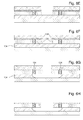
- the resonator 100 can be entirely made by etching in a wafer of the Silicon On Insulator (SOI) type.
- the wafer comprises a thick silicon substrate 102, an insulating silicon oxide intermediate layer 104, and a silicon top layer 106 in which the components of the MEMS oscillator according to the invention are formed, and in particular the resonator 100.
- structure of the resonator can first be etched into the upper silicon layer 106 to arrive at the result illustrated by the Figure 6A .
- the skilled person can achieve the engraving by any means that it seems appropriate.
- Figure 6A do not show them, it is preferably during this first step that the pads or connection pads are made and conductive tracks for connecting the components of the oscillator between them.
- the tracks may for example be formed by surface doping silicon.
- the tracks may for example be formed by metallizations deposited on the silicon.
- a dielectric layer 132 is then formed on the silicon, including on the vertical walls.
- the dielectric 132 is provided in particular to constitute the gate dielectric 124 ( figure 2 ).
- the dielectric layer 132 may be, for example, silicon dioxide formed by thermal oxidation of silicon. This oxide can then be removed locally at locations where it is not useful.
- the silicon dioxide is only one possibility among others for producing the dielectric layer 132.
- the SiO 2 can be replaced or combined with other dielectric material to, on the one hand, improve the dielectric constant, and on the other hand, to improve the selectivity during the engraving.
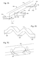
- FIGS. 7A, 7B and 7C are views a perspective of a second embodiment of the transistor resonator 300 according to the invention. Unlike the resonators 100 and 200 of the previous examples, the resonator 300 is designed to extend preferably in a vertical plane (perpendicular to a substrate).
- the resonator 300 is mainly formed of a vibrating beam 310 supported at its two ends by supports 312 and 314.
- the supports 312, 314 each comprise a foot 312a, 314a in doped silicon surmounted by a superstructure 312b , 314b.
- Each of the superstructures 312b, 314b comprises a piezoelectric material thickness 326.
- the two parts 326 of piezoelectric material are provided to vibrate the beam 310 in a particular vibration mode.
- the two parts 326 receive an excitation signal whose function is to alternately expand and contract each of the two thicknesses of piezoelectric material.
- the two parts 326 are preferably placed substantially at the ends of the beam 310.
- the transistor resonator 300 further comprises a piezoelectric sensing element 328 which is arranged in the center of the beam 310.
- the sensing piezoelectric element 328 has a substantially planar shape and is integral with the lower surface of the beam 310. Vibrating beam is intended to be excited at the first harmonic of its fundamental frequency.
- the standing wave produced by the vibration of the beam has two bellows separated by a node in the center of the beam.
- the piezoelectric element 328 integral with the center of the beam is subjected to considerable stretching constraints, while remaining virtually immobile.
- the Figure 7C schematically illustrates the polarization of the piezoelectric sensing element 328 when it is deformed by the vibration of the beam 310.
- the piezoelectric element 328 polarizes and depolarizes alternately. Since the space between the piezoelectric element and the well 330 is very narrow, the conductivity of the channel connecting the source region 308 to the drain region 309 is modulated by the cyclic electric field associated with the polarization of the piezoelectric element 328.
Landscapes
- Physics & Mathematics (AREA)
- Acoustics & Sound (AREA)
- Piezo-Electric Or Mechanical Vibrators, Or Delay Or Filter Circuits (AREA)
- Oscillators With Electromechanical Resonators (AREA)
- Micromachines (AREA)
Priority Applications (3)
| Application Number | Priority Date | Filing Date | Title |
|---|---|---|---|
| EP09177918A EP2330738A1 (de) | 2009-12-03 | 2009-12-03 | MEMS-Resonator mit Transistor und einen solchen Resonator umfassender Oszillator |
| PCT/EP2010/068249 WO2011067165A1 (fr) | 2009-12-03 | 2010-11-25 | Résonateur mems à transistor et oscillateur comportant un tel résonateur |
| TW99141473A TW201203852A (en) | 2009-12-03 | 2010-11-30 | MEMS transistor resonator and oscillator comprising such a resonator |
Applications Claiming Priority (1)
| Application Number | Priority Date | Filing Date | Title |
|---|---|---|---|
| EP09177918A EP2330738A1 (de) | 2009-12-03 | 2009-12-03 | MEMS-Resonator mit Transistor und einen solchen Resonator umfassender Oszillator |
Publications (1)
| Publication Number | Publication Date |
|---|---|
| EP2330738A1 true EP2330738A1 (de) | 2011-06-08 |
Family
ID=41697973
Family Applications (1)
| Application Number | Title | Priority Date | Filing Date |
|---|---|---|---|
| EP09177918A Withdrawn EP2330738A1 (de) | 2009-12-03 | 2009-12-03 | MEMS-Resonator mit Transistor und einen solchen Resonator umfassender Oszillator |
Country Status (3)
| Country | Link |
|---|---|
| EP (1) | EP2330738A1 (de) |
| TW (1) | TW201203852A (de) |
| WO (1) | WO2011067165A1 (de) |
Cited By (1)
| Publication number | Priority date | Publication date | Assignee | Title |
|---|---|---|---|---|
| US10483875B2 (en) | 2013-11-20 | 2019-11-19 | Industrial Technology Research Institute | Surface elastic wave generator, transceiver, and generation method thereof |
Families Citing this family (2)
| Publication number | Priority date | Publication date | Assignee | Title |
|---|---|---|---|---|
| DE112013006687B4 (de) * | 2013-03-28 | 2022-02-17 | Intel Corporation | Resonanzkanaltransistor mit mehreren gates |
| WO2022100828A1 (en) * | 2020-11-12 | 2022-05-19 | Huawei Technologies Co., Ltd. | Micromechanical resonator wafer assembly and method of fabrication thereof |
Family Cites Families (3)
| Publication number | Priority date | Publication date | Assignee | Title |
|---|---|---|---|---|
| US3413573A (en) | 1965-06-18 | 1968-11-26 | Westinghouse Electric Corp | Microelectronic frequency selective apparatus with vibratory member and means responsive thereto |
| MX9703801A (es) * | 1997-05-23 | 1998-11-30 | Ct Investig Y Estudios Del Ipn | Sensor de presion a tmos. |
| FR2901263B1 (fr) | 2006-05-18 | 2008-10-03 | Commissariat Energie Atomique | Dispositif sensible a un mouvement comportant au moins un transistor |
-
2009
- 2009-12-03 EP EP09177918A patent/EP2330738A1/de not_active Withdrawn
-
2010
- 2010-11-25 WO PCT/EP2010/068249 patent/WO2011067165A1/fr not_active Ceased
- 2010-11-30 TW TW99141473A patent/TW201203852A/zh unknown
Non-Patent Citations (3)
| Title |
|---|
| BECK R G ET AL: "GaAs/AlGaAs self-sensing cantilevers for low temperature scanning probe microscopy", APPLIED PHYSICS LETTERS, AIP, AMERICAN INSTITUTE OF PHYSICS, MELVILLE, NY, US LNKD- DOI:10.1063/1.122112, vol. 73, no. 8, 24 August 1998 (1998-08-24), pages 1149 - 1151, XP012022032, ISSN: 0003-6951 * |
| GROGG, D. ET AL: "Double gate movable body Micro-Electro-Mechanical FET as hysteretic switch: Application to data transmission systems", SOLID-STATE DEVICE RESEARCH CONFERENCE, 2008. ESSDERC 2008. 38TH EUROPEAN, 15 September 2008 (2008-09-15), Edinburgh, pages 302 - 305, XP002581913, ISBN: 978-1-4244-2363-7, DOI: 10.1109/ESSDERC.2008.4681758 * |
| LANGE D ET AL: "Electromagnetic actuation and MOS-transistor sensing for CMOS-integrated micromechanical resonators", SENSORS AND ACTUATORS A, ELSEVIER SEQUOIA S.A., LAUSANNE, CH LNKD- DOI:10.1016/S0924-4247(02)00307-2, vol. 103, no. 1-2, 15 January 2003 (2003-01-15), pages 150 - 155, XP004400394, ISSN: 0924-4247 * |
Cited By (1)
| Publication number | Priority date | Publication date | Assignee | Title |
|---|---|---|---|---|
| US10483875B2 (en) | 2013-11-20 | 2019-11-19 | Industrial Technology Research Institute | Surface elastic wave generator, transceiver, and generation method thereof |
Also Published As
| Publication number | Publication date |
|---|---|
| WO2011067165A1 (fr) | 2011-06-09 |
| TW201203852A (en) | 2012-01-16 |
Similar Documents
| Publication | Publication Date | Title |
|---|---|---|
| EP0587032B1 (de) | Intergrierter kapazitiver Wandler | |
| EP2074695B1 (de) | Siliziumresonator des stimmgabeltyps | |
| EP2437323B1 (de) | Vorrichtung zur Rückgewinnung von Druckenergie | |
| EP2112471A1 (de) | Montagevorrichtung für elektronisches Bauteil | |
| FR2898884A1 (fr) | Micro-capteur inertiel resonant a epaisseur variable realise en technologies de surface | |
| FR2864526A1 (fr) | Dispositif d'actionnement electrostatique | |
| WO2009076534A1 (en) | Resonant body transistor and oscillator | |
| FR2964651A1 (fr) | Dispositif a poutre suspendue et moyens de detection piezoresistive du deplacement de celle-ci, et procede de fabrication du dispositif | |
| EP2616386B1 (de) | In der ebene betätigte resonanzvorrichtung und verfahren zur herstellung der vorrichtung | |
| FR2828186A1 (fr) | Composant microelectromecanique | |
| WO2012034990A1 (fr) | Dispositif resonant, a detection piezoresistive et a resonateur relie de facon elastique au support du dispositif, et procede de fabrication de celui-ci | |
| FR3052765A1 (fr) | Dispositif microelectromecanique et/ou nanoelectromecanique a deplacement hors-plan comportant des moyens capacitifs a variation de surface | |
| FR2826645A1 (fr) | Composant microelectromecanique | |
| EP2330738A1 (de) | MEMS-Resonator mit Transistor und einen solchen Resonator umfassender Oszillator | |
| EP1637498B1 (de) | MOS Transistor mit verformbaren Gate | |
| FR3021309A1 (fr) | Dispositif microelectronique et/ou nanoelectronique capacitif a compacite augmentee | |
| EP3071932B1 (de) | Trägheitssensor mit verschachtelten seismischen massen und verfahren zur herstellung eines derartigen sensors | |
| CH702402A2 (fr) | Résonateur MEMS à transistor et oscillateur comportant un tel résonateur. | |
| FR2864951A1 (fr) | Dispositif de type microsysteme electromecanique a film mince piezoelectrique | |
| EP2201681B1 (de) | Auf nanometrischem oder mikrometrischem massstab vibrierende elektromechanische komponente mit verbessertem detektionsniveau | |
| WO2013007652A1 (fr) | Résonateur à ondes de volume exploitant l'excitation/détection de la vibration | |
| FR2857952A1 (fr) | Resonateur electromecanique et procede de fabrication d'un tel resonateur | |
| EP2600429B1 (de) | Schwingungsenergiesammler mit einem piezoelektrischen Keramikelement | |
| EP3459101A1 (de) | Mikroelektromechanischer schalter mit variabler funkfrequenz | |
| FR3122023A1 (fr) | Haut-parleur micrométrique |
Legal Events
| Date | Code | Title | Description |
|---|---|---|---|
| PUAI | Public reference made under article 153(3) epc to a published international application that has entered the european phase |
Free format text: ORIGINAL CODE: 0009012 |
|
| AK | Designated contracting states |
Kind code of ref document: A1 Designated state(s): AT BE BG CH CY CZ DE DK EE ES FI FR GB GR HR HU IE IS IT LI LT LU LV MC MK MT NL NO PL PT RO SE SI SK SM TR |
|
| AX | Request for extension of the european patent |
Extension state: AL BA RS |
|
| STAA | Information on the status of an ep patent application or granted ep patent |
Free format text: STATUS: THE APPLICATION IS DEEMED TO BE WITHDRAWN |
|
| 18D | Application deemed to be withdrawn |
Effective date: 20111209 |