EP2330865B1 - Dispositif de chauffage électrique - Google Patents
Dispositif de chauffage électrique Download PDFInfo
- Publication number
- EP2330865B1 EP2330865B1 EP09015002.0A EP09015002A EP2330865B1 EP 2330865 B1 EP2330865 B1 EP 2330865B1 EP 09015002 A EP09015002 A EP 09015002A EP 2330865 B1 EP2330865 B1 EP 2330865B1
- Authority
- EP
- European Patent Office
- Prior art keywords
- circuit board
- busbar
- printed circuit
- contact
- heating device
- Prior art date
- Legal status (The legal status is an assumption and is not a legal conclusion. Google has not performed a legal analysis and makes no representation as to the accuracy of the status listed.)
- Not-in-force
Links
Images



Classifications
-
- H—ELECTRICITY
- H05—ELECTRIC TECHNIQUES NOT OTHERWISE PROVIDED FOR
- H05B—ELECTRIC HEATING; ELECTRIC LIGHT SOURCES NOT OTHERWISE PROVIDED FOR; CIRCUIT ARRANGEMENTS FOR ELECTRIC LIGHT SOURCES, IN GENERAL
- H05B3/00—Ohmic-resistance heating
- H05B3/40—Heating elements having the shape of rods or tubes
- H05B3/42—Heating elements having the shape of rods or tubes non-flexible
- H05B3/48—Heating elements having the shape of rods or tubes non-flexible heating conductor embedded in insulating material
- H05B3/50—Heating elements having the shape of rods or tubes non-flexible heating conductor embedded in insulating material heating conductor arranged in metal tubes, the radiating surface having heat-conducting fins
-
- H—ELECTRICITY
- H05—ELECTRIC TECHNIQUES NOT OTHERWISE PROVIDED FOR
- H05K—PRINTED CIRCUITS; CASINGS OR CONSTRUCTIONAL DETAILS OF ELECTRIC APPARATUS; MANUFACTURE OF ASSEMBLAGES OF ELECTRICAL COMPONENTS
- H05K1/00—Printed circuits
- H05K1/02—Details
- H05K1/0213—Electrical arrangements not otherwise provided for
- H05K1/0263—High current adaptations, e.g. printed high current conductors or using auxiliary non-printed means; Fine and coarse circuit patterns on one circuit board
-
- H—ELECTRICITY
- H05—ELECTRIC TECHNIQUES NOT OTHERWISE PROVIDED FOR
- H05K—PRINTED CIRCUITS; CASINGS OR CONSTRUCTIONAL DETAILS OF ELECTRIC APPARATUS; MANUFACTURE OF ASSEMBLAGES OF ELECTRICAL COMPONENTS
- H05K3/00—Apparatus or processes for manufacturing printed circuits
- H05K3/30—Assembling printed circuits with electric components, e.g. with resistors
-
- H—ELECTRICITY
- H05—ELECTRIC TECHNIQUES NOT OTHERWISE PROVIDED FOR
- H05B—ELECTRIC HEATING; ELECTRIC LIGHT SOURCES NOT OTHERWISE PROVIDED FOR; CIRCUIT ARRANGEMENTS FOR ELECTRIC LIGHT SOURCES, IN GENERAL
- H05B2203/00—Aspects relating to Ohmic resistive heating covered by group H05B3/00
- H05B2203/02—Heaters using heating elements having a positive temperature coefficient
-
- H—ELECTRICITY
- H05—ELECTRIC TECHNIQUES NOT OTHERWISE PROVIDED FOR
- H05K—PRINTED CIRCUITS; CASINGS OR CONSTRUCTIONAL DETAILS OF ELECTRIC APPARATUS; MANUFACTURE OF ASSEMBLAGES OF ELECTRICAL COMPONENTS
- H05K1/00—Printed circuits
- H05K1/02—Details
- H05K1/0271—Arrangements for reducing stress or warp in rigid printed circuit boards, e.g. caused by loads, vibrations or differences in thermal expansion
-
- H—ELECTRICITY
- H05—ELECTRIC TECHNIQUES NOT OTHERWISE PROVIDED FOR
- H05K—PRINTED CIRCUITS; CASINGS OR CONSTRUCTIONAL DETAILS OF ELECTRIC APPARATUS; MANUFACTURE OF ASSEMBLAGES OF ELECTRICAL COMPONENTS
- H05K2201/00—Indexing scheme relating to printed circuits covered by H05K1/00
- H05K2201/09—Shape and layout
- H05K2201/09009—Substrate related
- H05K2201/09063—Holes or slots in insulating substrate not used for electrical connections
-
- H—ELECTRICITY
- H05—ELECTRIC TECHNIQUES NOT OTHERWISE PROVIDED FOR
- H05K—PRINTED CIRCUITS; CASINGS OR CONSTRUCTIONAL DETAILS OF ELECTRIC APPARATUS; MANUFACTURE OF ASSEMBLAGES OF ELECTRICAL COMPONENTS
- H05K2201/00—Indexing scheme relating to printed circuits covered by H05K1/00
- H05K2201/10—Details of components or other objects attached to or integrated in a printed circuit board
- H05K2201/10007—Types of components
- H05K2201/10166—Transistor
-
- H—ELECTRICITY
- H05—ELECTRIC TECHNIQUES NOT OTHERWISE PROVIDED FOR
- H05K—PRINTED CIRCUITS; CASINGS OR CONSTRUCTIONAL DETAILS OF ELECTRIC APPARATUS; MANUFACTURE OF ASSEMBLAGES OF ELECTRICAL COMPONENTS
- H05K2201/00—Indexing scheme relating to printed circuits covered by H05K1/00
- H05K2201/10—Details of components or other objects attached to or integrated in a printed circuit board
- H05K2201/10227—Other objects, e.g. metallic pieces
- H05K2201/10272—Busbars, i.e. thick metal bars mounted on the printed circuit board [PCB] as high-current conductors
-
- H—ELECTRICITY
- H05—ELECTRIC TECHNIQUES NOT OTHERWISE PROVIDED FOR
- H05K—PRINTED CIRCUITS; CASINGS OR CONSTRUCTIONAL DETAILS OF ELECTRIC APPARATUS; MANUFACTURE OF ASSEMBLAGES OF ELECTRICAL COMPONENTS
- H05K2201/00—Indexing scheme relating to printed circuits covered by H05K1/00
- H05K2201/10—Details of components or other objects attached to or integrated in a printed circuit board
- H05K2201/10227—Other objects, e.g. metallic pieces
- H05K2201/10386—Clip leads; Terminals gripping the edge of a substrate
Definitions
- the present invention relates to an electrical heating device, in particular a heating device for a motor vehicle, comprising a heating block comprising at least one heat-emitting element, which is thermally conductively connected to a heat-generating element comprising at least one PTC element.
- the electric heater further includes a housing for housing the heater block and a controller provided in a structural unit with the heater block.
- a circuit board is provided which is equipped with components and contacted with at least one busbar.
- Such an electric heater is, for example, from the date of the present applicant EP 1 253 808 A2 known.
- the structural unit is regularly ensured by a housing formed of plastic, which accommodates both the heating block and the control device in itself.
- the housing may be formed in several parts.
- the busbars are manufactured as part of the structure of the circuit board by the electronics manufacturer and provided on the circuit board.
- the attachment of the busbar is accordingly with connection and fastening techniques that are familiar to the electronics manufacturer.
- a relatively high cost is usually necessary to connect the busbar to the circuit board.
- the busbar must not only be electrically connected to selected areas of the circuit board. Rather, it is also necessary, provided on the busbar connection contacts for the power or load current with the necessary strength on the circuit board directly or indirectly to be fastened via the busbar.
- the high vibration load which has to endure a generic electric heater when used in a motor vehicle, here makes special demands on the connection technology. Inadequate connection can lead to contact resistance between the
- the present invention has for its object to provide a generic electric heater that can be easier and more economical, but without affecting the requirements to be made of the electrical contact between the circuit board and the busbar can be produced.
- the present invention further intends to specify a printed circuit board which can be used in particular in a generic electric heating device and which is contacted with the busbar in a simple and reliable manner.
- the present invention provides a heater having the features of claim 1.
- the busbar first and second pads forms, the first pads with a first surface of the circuit board and the second pads interact with a second surface of the circuit board.
- the busbar is provided according to the invention on both sides of the circuit board. In other words, the bus bar has areas located on the first surface of the circuit board, whereas other areas are on the second surface of the circuit board.
- the invention is based in particular on the fact that the busbar is supported on the printed circuit board via at least two supporting points. These support points are formed by supports which are formed by predetermined portions of the busbar. If this predetermined portion is applied over a large area to the printed circuit board, this large-area section forms two editions in the context of the present invention. Usually, however, at least two separate and in relation to the total surface area of the busbar relatively small first and two second pads are formed by the busbar, with the opposite to the realization of the present invention Interact surfaces of the circuit board. This takes into account the circumstance that the busbar can sometimes be deformed by thermal and / or mechanical influences relative to the printed circuit board.
- the attachment of the at least one busbar to the circuit board via at least two support points on each of the two surfaces of the circuit board is to create a certain compensation possibility, without putting the circuit board itself under tension.
- the pads can interact at very different locations with the circuit board.
- recesses may be provided in the printed circuit board, through which the busbar is passed from one to the other surface of the circuit board.
- the first and the second edition of the bus bar may be formed as a claw which engages around the circuit board.
- a contacted with claws on the circuit board conductor rail may have only two spaced apart provided claws for their attachment and are fixed by lateral pushing against the circuit board with this and contacted.
- the claw usually comprises two spaced-apart first pads and a second pad provided therebetween.
- the lateral distance of the first pads is preferably chosen so that the second edition is justified with a certain small material loss, which is due to the punching of the pads from a sheet metal forming the busbar and bending the pads to form a the thickness of the circuit board corresponding claw spacing however, is provided substantially immediately adjacent to the first jaw.
- the cooperating with the circuit board surfaces of the pads can be additionally formed so that the pads have at least at the point where the pads also serve the electrical contact between the busbar and the circuit board, formed by forming projection, the punctual and accordingly in predetermined manner abuts against the surface of the circuit board to a conductor provided there.
- Such a trained by forming survey also causes the claw is slightly elastically applied when pushed onto the circuit board against the opposite surfaces of the circuit board. As a result, a force or frictional retention of the busbar is achieved on the circuit board, which may be sufficient for itself to secure the busbar to the circuit board.
- the present invention teaches, in particular, only attachment of the one or all bus bars to the printed circuit board, which is initially implemented for assembly purposes.
- the preassembled circuit board can then be equipped, for example, with electrical and electronic components. Thereafter, for example, by vapor phase soldering a permanent and cohesive connection of the components and the one or all busbars on the circuit board done.
- the completed electric heating device then has one or more bus bars, which are initially connected by interaction of first and second supports with the first and second surfaces of the circuit board with this frictional, force and / or positive fit, by connecting elements alone are formed by the circuit board and the busbar, and in addition, a regularly effected by soldering cohesive connection at least in the areas in which the busbar is also electrically contacted with the conductor track, ie soldered to the circuit board.
- first and second pads, which are provided on the bus bar serve only for mechanical locking, i. are not electrically contacted with a conductor of the circuit board and there are not soldered to the circuit board.
- At least one recess in which a power transistor is accommodated is provided on the circuit board.
- the at least one contact rail forms in the recess an exposed there contact surface on which the power transistor is mounted.
- this attachment is carried out in an electrically conductive manner, so that an electrical contact is effected between the busbar and the power transistor via the contact surface.
- the recess provided in the printed circuit board is used in this preferred development to guide the busbar from one to the other surface through the printed circuit board.
- the busbar preferably has first and second pads adjacent to the contact surface.
- the circuit board therefore acts on one side usually close to the edge of the recess with a first support and a second support together.
- the recess may be an edge-open U-shaped recess. In this preferred development claws are usually provided to connect the busbar to the circuit board in the region of the recess.
- the recess may, however, be a recess circumferentially surrounded by the material of the circuit board, in which the power transistor is received
- the bus bar has a projecting from the circuit board cooling vane, which is dimensioned such that it fits through the recess.
- the vote of the dimension of the cooling vane on the dimension of the recess takes place with the aim of providing the cooling lance through the recess laterally projecting the circuit board.
- the cooling lug can protrude from the latter in a direction transverse to the direction of extension of the printed circuit board.
- the cooling lug is provided so that it also projects beyond the circuit board laterally, so that a cooling air flow flowing against the cooling lug can laterally pass through the circuit board.
- cooling lugs With regard to a compact design of the circuit board, however, a preference is given to a solution in which the cooling vanes are wholly or partially outside the envelope, which surrounds the circuit board. With the present invention, an alignment of the cooling lugs provided as sheet metal strip parallel to the plane of the circuit board is considered to be preferred.
- a good support of the printed circuit board in the area of the contact surface is created in accordance with a preferred development of the present invention in that the busbar between the cooling lug and the contact surface forms a first contact and adjacent to the contact surface on the opposite side of the cooling lug a contact surface near second support.
- first and second supports or first and second surfaces it is merely intended to express that they are different sides of the conductor track or of the sections of the conductor rail cooperating with these different sides is.
- the refinement yields the advantage that the busbar usually interacts with the printed circuit board immediately adjacent to the cutout, so that the busbar is fixed in the area forming the contact surface for the power transistor in a predetermined manner relative to the printed circuit board.
- a plurality of recesses are preferably provided side by side and the contact rail forms a plurality of contact surfaces, each exposed in one of the recesses.
- adjacent contact surfaces are connected to one another via a connecting web forming a second support.
- the cooling lug usually goes from the first surface and is supported on this.
- the attachment of the busbar takes place in any case via locking elements.
- a certain form-fitting positioning of the busbar is usually first achieved.
- the busbar is additionally locked by one or more locking connections relative to the printed circuit board, a sufficient positioning and fastening of the busbar is provided on the circuit board, which later only needs to be secured by a few solder joints.
- the aforementioned latching connection is preferably realized by a latching leg which comprises a latching leg base extending parallel to and spaced from the second surface and a latching leg flap extending substantially at right angles to this latching leg base and passing through a latching opening of the circuit board.
- This locking leg lug has a latching against the first surface locking cams.
- About the locking leg base a certain distance from the surface of the circuit board is provided to provide in particular the locking leg lug with an extension substantially perpendicular to the surface extension of the circuit board and at a distance to other parts of the busbar.
- a very good definition of the busbar by the locking leg is achieved according to a preferred embodiment, in which the locking leg forms a support leg which is arcuate in the direction of the circuit board and adjacent to the locking hole abuts against the circuit board.
- the plant leg usually forms with its formed by cutting back against the locking leg flap frontal end of a first edition, which cooperates with the second surface of the circuit board, whereas the locking cam locked against the first surface, so that the busbar in the region of the locking leg between the plant leg and the locking cam by the locking leg is encompassed.
- the locking opening and the locking leg luff are matched to one another such that the locking leg lug is only slightly movable within the locking opening, so that the busbar is fixed via the locking leg with high accuracy relative to the circuit board.
- the locking leg of a provided at a distance from the circuit board busbar base portion which forms the contact surface on the contact surface near the second edition.
- This busbar is therefore preferably designed so that only the at least one contact surface is at the level of the printed circuit board, whereas the remaining provided within the envelope surface of the printed circuit board region of the busbar is provided almost exclusively at a distance from the circuit board.
- the area of the busbar provided outside the envelope surface forms the at least one cooling lug.
- the corresponding busbar is thereafter optimally thermally isolated from the circuit board and can deliver heat to surrounding air over almost its entire area except the contact surface (s).
- the preferred development has in particular an elongated busbar base portion from which comb-like usually depart a plurality of transverse webs, which initially form the contact surfaces for the power transistors and in the further course in each case the cooling vanes.
- this preferably has contact points formed by forming the metal strip forming the busbar.
- the support points are usually located in the middle of the regularly elongate busbar base portion and contact only slightly, preferably selectively the circuit board. By these support points, the busbar is supported at a distance from the circuit board at this.
- the support points are preferably at the height of the transverse webs.
- All previously described functional surfaces of a busbar are usually formed by punching, bending or stamping a metal strip.
- the circuit board has a plurality of side by side provided receiving slots for tabs, which electrically connect the heating block with the circuit board.
- the circuit board of the busbar base portion covers these receiving slots completely or partially. This means that the receiving slots in an orthogonal plan view of the circuit board from the side on which the busbar is, the receiving slots are not fully visible anyway.
- the bus bar base portion extends perpendicular to the longitudinal extent of the receiving slots and leaves no more than 30% of the length of the receiving slots.
- the electrical heating device preferably has at least two busbars which form connecting lugs arranged adjacent to one another and aligned at right angles to the printed circuit board.
- Each of the two busbars regularly forms a single connection lug.
- the development differs in that a contact tongue piece is attached to at least one of the terminal lugs.
- each busbar is formed at least two pieces.
- the busbar on the one hand and the contact piece on the other hand can be made of different materials and / or provided with special coatings.
- the contact tongue piece preferably has a coating of tin, silver or nickel.
- the busbar and / or the contact tongue piece can be formed from copper, a copper alloy or even a brass alloy. It is also conceivable embodiment of the busbar and / or the contact tongue piece of aluminum or an aluminum alloy with a solderable surface, for. B. nickel plated.
- the housing With a view to a reliable positioning of the control device in the housing, it is proposed according to a preferred embodiment of the present invention to form the housing with a housing base in which the heating block and the contact lugs are received and which with the tabs and slightly surmounted by the contact lugs contact tab recordings connected is. On these contact flags shots is the circuit board on.
- the housing base is usually made by means of plastic injection molding, wherein the contact lugs recordings are preferably provided integrally by means of injection molding on the housing base.
- the housing base is usually closed by a unitary housing cover, which leaves open in the region of the heating block one or more passage openings for the air flowing through the heating block, further separate separateméfahneningö réelleen extending between the heating block and a housing portion which receives the control device, and a further portion which closes a control housing integrally formed on the housing base.
- the contact tab receptacles are preferably open to a dividing plane of the housing, so that the heating block can be inserted together with the contact lugs in the housing base. Transverse to the plane of the heating block, the tabs are slightly surmounted by the tabs. Since in this area, the circuit board rests, the penetration of the circuit board by the contact lug is exactly predetermined.
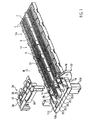
- FIG. 1 shows a perspective side view of an embodiment of an electric heater with a heating block 2, which comprises a layered structure consisting of several heat-emitting elements 4 provided between the heat-emitting elements 4 heat-generating elements 6.
- parts of the heating block 2 have been omitted in the central region of the embodiment, so that several in a plane of the layer structure provided in succession PTC elements 8 can be seen and a metal strip 10 to which these PTC elements heat-conducting and electrically conductive abut.
- a further sheet-metal strip is provided on the other side of the sheet-metal strip 10, so that the PTC elements 8 are contacted via the two sheet-metal strips 10.
- the heating block 2 is clamped in the embodiment shown under spring tension in a housing base part 12, so that all layers of the heating block 2 are applied by the force of the spring device against each other.
- the lower housing part 12 comprises a Bankblockgepurteil 12 a and a control housing part 12 b, which are integrally provided with each other and between which cooling lance receiving openings 14 between the two housing parts 12 a, 12 b connecting webs 16 are formed.
- the webs 16 are aligned with contact tab receptacles 18 which are provided in the control housing part 12b. There, the tab receptacles 18 are only upper side, i. in the direction of the air flow, marked with the arrow "L", are open.
- Selected metal strips 10 of the heating block 2 are passed through the webs 16 into the contact lugs 18 record and form there marked with reference numerals 20.1 - 20.3 and 20.4 and 20.5 contact lugs.
- the tabs 20 slightly project beyond the tab receptacles 18, i. are exposed above the predetermined by the lower housing part 12 dividing plane.
- this dividing plane is also surmounted by parts of a fastening flange 22 for the electrical heating device, which is provided approximately at the level of the control housing part 12b.
- housing base 12 is closed after mounting all components of the electric heater with a housing cover, which also completes the then surrounding the housing circumferentially mounting flange 22.
- the housing cover forms both a cover for the heating block 2 as well as a designated by reference numeral 24 control device and closes this tight.
- the control housing 12b is sealed by a molded-on to the housing base 12 seal 26 in the region of the openings for the contact lugs 10 to a ventilation duct, which leads to the air flow L to be heated.
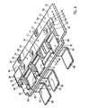
- control device 24 will be described with particular reference to FIGS FIGS. 2 to 5 explained in more detail.
- the control device 24 has two bus bars 28, 30 which are mounted on a printed circuit board 32.
- the printed circuit board 32 carries components, for example in the form of power transistors 34 (see. FIG. 5 ), which are contacted via conductor tracks formed by the printed circuit board 32.
- a plurality of receiving slots 36 are recessed parallel to each other and at the same height.
- contact elements 40 are mounted on the printed circuit board 32 with spring webs projecting into the receiving slots 36.
- the contact elements 40 have a flange which rests on a surface of the printed circuit board 32 referred to below as the first surface 42 (cf. FIG. 5 ).
- the contact elements 40 form electrical connection elements 44.1-44-6 for printed conductors of the printed circuit board 32.
- FIG. 5 the printed circuit board 32 after soldering all the functional elements 28, 30, 34, 44 by means of vapor phase soldering reveal the Figures 2-4 an intermediate step in the production of the circuit board 32 and illustrate the proposed with the invention, basically positive connection of the bus bars 28, 30 to the circuit board 32 to solder the bus bars 28, 30 with the circuit board 32nd
- the busbar referred to below as the first busbar 30 extends essentially at right angles to the printed circuit board 32 and is provided at the edge for this purpose.
- the first busbar 30 projects beyond the first surface 42 of the printed circuit board 32.
- two jaws 46 are formed on the first busbar 30 and embrace the printed circuit board 32.
- Each claw 46 comprises webs cut free first by cutting, of which the two exteriors are formed by bending over as first jaw pads 48, whereas the middle, longer web is deformed by bending over to a second jaw pad 50.
- the first and second jaw pads 48, 50 extend parallel to each other and parallel to the first surface 42 and a second surface, respectively 52 of the printed circuit board 32.
- the circuit board 32 is provided with two claw recesses 54. Each of the claw recesses 54 receives the web forming the second jaw pads 50. As a result, the first busbar 30 is positioned in its longitudinal direction and held in a form-fitting manner relative to the printed circuit board 32.
- the printed circuit board 32 facing away from the back of the second jaw support 50 is provided by forming a recess 56 which forms on the circuit board 32 side facing a contact curvature over which the first bus bar 30 provided on the second surface 52 of the circuit board 32 Tracks is contacted.
- the printed circuit board 32 slides on the edge side against inclined surfaces which are formed by these contact curvatures, so that the claws 46 are resiliently biased against the printed circuit board 32.
- connection tab 58 This in FIG. 2 rear end of the first bus bar 30 is bent at right angles and forms a connection tab 58, which projects beyond the circuit board 32.
- This busbar 28 is formed from a first comb-like cut sheet metal strip and has a parallel to the longitudinal extent of the circuit board 32 extending busbar base 60, from the three webs 62 exit at right angles.
- the webs 62 form three parallel to the circuit board 32 extending portions which are formed by bending the metal strip.
- a first relatively short region lies at the same height as the plane of the busbar base 60 and, by double bending, transitions into a contact surface 64, which slightly projects beyond the first surface of the printed circuit board 32 and extends parallel to it (cf. FIG. 2 ).
- each web forms inner second pads 68 which cooperate with, ie, support, the second surface 52.
- an outer first support 70 is formed by bending the webs 62, which are supported near the circuit board edge on the first surface 42 of the circuit board 32 (see, in particular FIG. 2 ).
- the contact surfaces 64 are located in a formed on the circuit board 32 recesses 72. Between the recesses 72, the sheet material of the second bus bar 28 forms connecting webs 74 which extend transversely to the webs 62 and connect the contact surfaces 64 together. These connecting webs 74 form transversely extending second pads 76, which cooperate with the second surface 52 of the printed circuit board 32. In the extension of these connecting webs 74, the contact surfaces 64 on the outside projecting support webs 78 are formed by the sheet material, forming the near-recess second pads 80, which cooperate with the second surface 52. For receiving the connecting webs 74 and the support webs 78, the recesses 72 are provided for the contact surfaces 64 at their opposite longitudinal edges with web recesses 82.
- busbar base 60 At the level of the webs 62 support points 84 are formed on the busbar base 60 by local forming, which are supported on the second surface 52 of the circuit board 32. As a result, the busbar base 60 is spaced apart from the second surface 52 of the printed circuit board 32. In the longitudinal direction of the busbar base 60, the sheet material of the second busbar 28 forms latching legs 86, 88.
- Front locking leg 86 shown has a extending in the plane of the busbar base 60 locking leg base 90, depart from the two right angles arcuate segments.
- a longer segment forms a locking leg lug 92, which is bent around 90 ° relative to the locking leg base and a locking opening 94 passes through, which is recessed in the circuit board 32.
- the free end of the locking leg lug is provided with a locking cam 94 which is formed by punching and bending the sheet material and protrudes from the locking leg tab 92 and the first surface 42 engages over, so that the locking leg 86 is secured captive against the circuit board 32.
- the locking leg base has a shorter length than the locking leg lug 92 and is also at 90 ° to form a plant leg 98 whose front end extends parallel to the second surface 52 of the circuit board 32 and there forms a latching pad 100, so that the Printed circuit board 32 between the latching pad 100 and / or the locking cam 94 comes to rest.
- the locking leg 88 is formed, only with the difference that the locking leg base 90 is not formed at the free end of the busbar base 60, but first by free cutting a parallel to this locking leg base 90 extending Sheet metal strip inward, ie cut out to the center of the busbar base 60 and then folded around and punched.
- the free end of the busbar base 60 is at right angles arc around the formation of a positive terminal tab 102 (see. Figures 2 and 3 ).
- the two bus bars 28, 30 are first prepared by punching and bending in the manner described.
- the second busbar 30 is pushed laterally onto the printed circuit board 32. It then surrounds the printed circuit board 32 non-positively and is held in a form-fitting manner within the claw recesses 54.
- the elastic bias within the jaws 46 secures the bus bar 30 opposite the circuit board 32.
- the other bus bar 28 is first passed through the respective recesses 72 with their cooling vanes 66 forming free ends.
- the second busbar 28 is guided obliquely positioned relative to the printed circuit board 32.
- the second bus bar 28 is then held positively against the circuit board 32 in the insertion direction.
- the bus bar 28 is pivoted in the direction of the circuit board 32.
- the locking leg flaps 92 engage in the locking openings 94 until the circuit board is locked to the locking legs 86, 88.
- both bus bars 28, 30 are held by the interaction of the first and second pads positively on the circuit board 32.
- the preassembled printed circuit board 32 in this way is then usually forwarded to the so-called electronics manufacturing, where by means of vapor phase soldering, the components 34 are applied to the contact surfaces 64 to connect the power transistors 34 with good heat conduction with the cooling vanes 66.
- Contact feet 104 of the power transistors 34 are soldered to printed conductors of the printed circuit board 32.
- the busbars 28, 30 are soldered in any case at their contact points to conductor tracks of the printed circuit board 32 with this.
- contact tongue pieces 106, 108 are soldered to the terminal lugs 58, 102. These contact lugs 106, 108 are adapted to a female connector for electrical connection of the embodiment of the 12-volt electrical system accordingly.
- a control connector housing 110 is mounted on the circuit board 32 in electronics manufacturing and plug contact elements within the control connector housing 110 provided for the connection of a control cable to the circuit board 32 electrically conductive to the circuit board 32.
- control device 24 is inserted into the control housing part 12a.
- the individual contact lugs 20.1 to 20.6 are introduced into the associated electrical connection elements 44.1 to 44.6.
- the flanges of the associated contact elements 40 then rest on the edge of the contact tab receptacles 18.
- a lower support with the bottom of the control housing part 12 b is formed by the free end face of the first bus bar 30.
- the control device 24 is positioned in the control housing part 12b.
- the cooling vanes 66 project beyond the control housing part 12b and are exposed in the cooling airfoil receiving openings.
- the contact lugs 106, 108 are located in a recessed on the housing base 12 power connector housing 12c.
- the control connector housing 110 extends through an opening 112 recessed in the bottom of the control housing 12b.
- the control device 24 is designed to save space in its surface projecting over the surface of the lower housing part 12, since the second bus bar 28 projects slightly beyond the printed circuit board 32, but at least partially covers the receiving slots 36 in the longitudinal direction of the layers of the heating block 2, then the control device 24 Also formed in the longitudinal direction of the layers of the heating block 2 is compact.
- the first bus bar 28 forms the positive pole of the current supply for the electric heater; the first busbar 30 from the ground pole.
- the power transistors 34 switch on the ground side, to which the electrical connection elements 44.1, 44.4 and 44.5 are connected.
- the other electrical connection elements 44.2, 44.3 and 44.6 are assigned to the positive busbar electrically.
Landscapes
- Engineering & Computer Science (AREA)
- Microelectronics & Electronic Packaging (AREA)
- Manufacturing & Machinery (AREA)
- Coupling Device And Connection With Printed Circuit (AREA)
Claims (13)
- Dispositif de chauffage électrique, notamment dispositif de chauffage électrique pour un véhicule automobile, comprenant un bloc chauffant (2) comportant au moins un élément (4) émettant de la chaleur, qui est relié de façon à transmettre la chaleur avec un élément de production de chaleur (6) comportant au moins un élément PTC (à coefficient de température positif) (8), le dispositif comprenant également un boitier (12) destiné à accueillir le bloc chauffant (2) et un dispositif de commande (24) prévu de manière à former une unité de construction avec le bloc chauffant (2), le dispositif de commande comportant une plaque de circuit imprimé (32), qui est équipée de composants (34) et est en contact avec au moins une barrette de courant ou de connexion (28, 30),
caractérisé
en ce que la barrette de connexion (28, 30) forme des premiers appuis (48, 70) et des deuxièmes appuis (50, 68, 76, 80, 82, 100), les premiers appuis (48, 70) coopérant avec une première surface (42) de la plaque de circuit imprimé (32), et les deuxièmes appuis (50, 68, 76, 80, 82, 100) avec une deuxième surface (52) de la plaque de circuit imprimé (32), et
en ce que la plaque de circuit imprimé (32) présente au moins un évidement (72),
en ce que la barrette de connexion (28) forme une surface de contact (64) librement dégagée dans l'évidement (72) et sur laquelle est fixée un transistor de puissance (34), et
en ce que la barrette de connexion présente les premiers et deuxièmes appuis (70; 68, 76, 80) au voisinage de ladite surface de contact (64). - Dispositif de chauffage électrique selon la revendication 1, caractérisé en ce que les premiers et deuxièmes appuis (48; 50) de la barrette de connexion (30) forment une griffe (46) qui enserre la plaque de circuit imprimé (32).
- Dispositif de chauffage électrique selon la revendication 2, caractérisé en ce que la griffe (46) comprend deux premiers appuis (48) prévus à distance l'un de l'autre et un deuxième appui (50) prévu entre les deux précédents.
- Dispositif de chauffage électrique selon l'une des revendications précédentes, caractérisé par une ailette de refroidissement (66), qui fait saillie de la plaque de circuit imprimé (32) et est formée par la barrette de connexion (28), et qui est conçue pour pouvoir passer à travers l'évidement (72).
- Dispositif de chauffage électrique selon la revendication 4, caractérisé en ce que la barrette de connexion (28) forme entre l'ailette de refroidissement (66) et la surface de contact (64), un premier appui (70), et au voisinage de la surface de contact (64), sur le côté opposé à celui où se trouve l'ailette de refroidissement (66), un deuxième appui (68) proche de la surface de contact.
- Dispositif de chauffage électrique selon l'une des revendications précédentes, caractérisé en ce que sont prévus plusieurs évidements (72), et en ce que la barrette de connexion (28) forme plusieurs surfaces de contact (64), qui sont chacune librement dégagées dans l'un des évidements (72), et en ce que des surfaces de contact (64) voisines sont reliées mutuellement par l'intermédiaire d'une nervure de liaison (74) formant un deuxième appui (76).
- Dispositif de chauffage électrique selon l'une des revendications précédentes, caractérisé en ce que la barrette de connexion (28) présente une branche d'encliquetage (86, 88), qui comprend une base de branche d'encliquetage (90) s'étendant parallèlement et à distance de la deuxième surface (52), et une languette de branche d'encliquetage (92) s'étendant sensiblement de manière perpendiculaire à la base de branche d'encliquetage (90), traversant une ouverture de verrouillage (94) de la plaque de circuit imprimé (32), et comportant un cran d'encliquetage (96) verrouillant contre la première surface (42).
- Dispositif de chauffage électrique selon la revendication 7, caractérisé en ce que la branche d'encliquetage (86) présente une branche d'appui (98), qui est repliée en direction de la plaque de circuit imprimé (32) et s'appuie contre la plaque de circuit imprimé (32) au voisinage de l'ouverture de verrouillage (94).
- Dispositif de chauffage électrique selon la revendication 7 ou la revendication 8, caractérisé en ce que la branche d'encliquetage (86) est issue d'un tronçon de base de barrette de connexion (60) prévu à distance de la plaque de circuit imprimé (32), et qui forme la surface de contact (64) par l'intermédiaire du deuxième appui (68) proche de la surface de contact.
- Dispositif de chauffage électrique selon la revendication 9, caractérisé en ce que la base de barrette de connexion (60) s'appuie sur la plaque de circuit imprimé (32) à distance de celle-ci, par des points d'appui (84) réalisés par déformation d'une bande de tôle formant la barrette de connexion (28).
- Dispositif de chauffage électrique selon la revendication 9 ou la revendication 10, caractérisé en ce que la plaque de circuit imprimé (32) présente plusieurs fentes d'accueil (36) prévues côte à côte et destinées à des pattes de contact (20), qui raccordent électriquement le bloc chauffant (2) à la plaque de circuit imprimé (32) et sont recouvertes, au moins partiellement, par la base de barrette de connexion (60).
- Dispositif de chauffage électrique selon l'une des revendications précédentes, caractérisé en ce que sont prévues au moins deux barrettes de connexion (28, 30), qui forment des pattes de raccordement (58, 102) agencées au voisinage les unes des autres et orientées perpendiculairement à la plaque de circuit imprimé (32), et en ce que sur l'une au moins des pattes de raccordement (58, 102) est fixée une pièce de languette de contact (106, 108).
- Dispositif de chauffage électrique selon l'une des revendications précédentes, caractérisé en ce que le boitier comprend une base de boitier (12) dans laquelle sont logés le bloc chauffant (2) et les pattes de contact (20), et qui est reliée à des logements de pattes de contact (18) accueillant les pattes de contact (20) et dont dépassent légèrement les pattes de contact (20), et sur lesquels repose la plaque de circuit imprimé (32).
Priority Applications (1)
| Application Number | Priority Date | Filing Date | Title |
|---|---|---|---|
| EP09015002.0A EP2330865B1 (fr) | 2009-12-03 | 2009-12-03 | Dispositif de chauffage électrique |
Applications Claiming Priority (1)
| Application Number | Priority Date | Filing Date | Title |
|---|---|---|---|
| EP09015002.0A EP2330865B1 (fr) | 2009-12-03 | 2009-12-03 | Dispositif de chauffage électrique |
Publications (2)
| Publication Number | Publication Date |
|---|---|
| EP2330865A1 EP2330865A1 (fr) | 2011-06-08 |
| EP2330865B1 true EP2330865B1 (fr) | 2015-10-21 |
Family
ID=41720562
Family Applications (1)
| Application Number | Title | Priority Date | Filing Date |
|---|---|---|---|
| EP09015002.0A Not-in-force EP2330865B1 (fr) | 2009-12-03 | 2009-12-03 | Dispositif de chauffage électrique |
Country Status (1)
| Country | Link |
|---|---|
| EP (1) | EP2330865B1 (fr) |
Cited By (5)
| Publication number | Priority date | Publication date | Assignee | Title |
|---|---|---|---|---|
| WO2020239045A1 (fr) * | 2019-05-31 | 2020-12-03 | Valeo Automotive Air Conditioning Hubei Co., Ltd. | Dispositif de chauffage |
| US20220361295A1 (en) * | 2019-09-30 | 2022-11-10 | Valeo Automotive Air Conditioning Hubei Co. Ltd. | A heating device |
| EP3977021A4 (fr) * | 2019-05-31 | 2023-06-28 | Valeo Automotive Air Conditioning Hubei Co., Ltd. | Dispositif de chauffage |
| EP3702691B1 (fr) * | 2019-02-28 | 2023-11-15 | Gerdes Holding GmbH & Co. KG | Chauffe-eau instantané pour réchauffer un liquide |
| FR3149144A1 (fr) * | 2023-05-26 | 2024-11-29 | Valeo Systemes Thermiques | Dispositif de chauffage électrique relié à la masse par un élément de connexion d’un dispositif électronique de commande. |
Families Citing this family (14)
| Publication number | Priority date | Publication date | Assignee | Title |
|---|---|---|---|---|
| DE102011089539B3 (de) * | 2011-12-22 | 2013-04-25 | Behr-Hella Thermocontrol Gmbh | Vorrichtung zur Ansteuerung einer elektrischen Heizung für Fahrzeuge und elektrische Heizung mit einer derartigen Vorrichtung |
| FR3004058B1 (fr) * | 2013-03-26 | 2016-12-16 | Valeo Systemes Thermiques | Module de commande d'un appareil electrique |
| FR3004056B1 (fr) * | 2013-03-26 | 2016-10-21 | Valeo Systemes Thermiques | Module de commande d'un appareil electrique |
| FR3004057B1 (fr) * | 2013-03-26 | 2017-02-17 | Valeo Systemes Thermiques | Module de commande d'un appareil electrique |
| EP2881678A1 (fr) * | 2013-12-03 | 2015-06-10 | Mahle Behr France Rouffach S.A.S | Chauffage électrique |
| EP2933577B1 (fr) | 2014-04-14 | 2017-12-06 | Mahle Behr France Rouffach S.A.S | Dispositif de chauffage électrique |
| DE202014011300U1 (de) * | 2014-04-30 | 2019-02-28 | Ellenberger & Poensgen Gmbh | Elektrische Schaltung |
| FR3082693A1 (fr) * | 2018-06-13 | 2019-12-20 | Valeo Systemes Thermiques | Dispositif d'alimentation pour radiateur electrique et radiateur comprenant un tel dispositif |
| CN109640403B (zh) * | 2018-12-14 | 2022-05-27 | 博耐尔汽车电气系统有限公司 | 一种ptc加热器电源装置及其装配工艺 |
| DE102019200021B4 (de) * | 2019-01-03 | 2023-10-12 | Zf Friedrichshafen Ag | Kontaktierungsvorrichtung |
| CN114269077B (zh) * | 2021-12-27 | 2024-03-12 | 欣强电子(清远)有限公司 | 一种pcb硬板弯折方法及其使用的弯折设备 |
| DE102022123568A1 (de) | 2022-09-15 | 2024-03-21 | Eberspächer Catem Gmbh & Co. Kg | Steuervorrichtung und Verfahren zur Herstellung einer Steuervorrichtung |
| DE102022005120A1 (de) | 2022-09-15 | 2024-03-21 | Eberspächer Catem Gmbh & Co. Kg | Steuervorrichtung |
| DE102024108924B4 (de) * | 2024-03-28 | 2026-02-05 | Borgwarner Inc. | Durchlauferhitzer und Heizplatte für einen Durchlauferhitzer |
Family Cites Families (5)
| Publication number | Priority date | Publication date | Assignee | Title |
|---|---|---|---|---|
| US4536826A (en) * | 1984-09-10 | 1985-08-20 | At&T Bell Laboratories | Snap-in bus bar |
| JPH09307202A (ja) * | 1996-05-20 | 1997-11-28 | Mitsubishi Electric Corp | 混成集積回路 |
| JP3457239B2 (ja) * | 1999-11-24 | 2003-10-14 | 株式会社オートネットワーク技術研究所 | 電気接続箱における回路形成方法および回路の接続構造 |
| ES2254568T3 (es) * | 2000-05-23 | 2006-06-16 | CATEM GMBH & CO.KG | Dispositivo calefactor electrico, especialmente para la aplicacion de automoviles. |
| JP4131724B2 (ja) * | 2004-10-18 | 2008-08-13 | Tdk株式会社 | 回路基板への端子の取付構造 |
-
2009
- 2009-12-03 EP EP09015002.0A patent/EP2330865B1/fr not_active Not-in-force
Cited By (6)
| Publication number | Priority date | Publication date | Assignee | Title |
|---|---|---|---|---|
| EP3702691B1 (fr) * | 2019-02-28 | 2023-11-15 | Gerdes Holding GmbH & Co. KG | Chauffe-eau instantané pour réchauffer un liquide |
| WO2020239045A1 (fr) * | 2019-05-31 | 2020-12-03 | Valeo Automotive Air Conditioning Hubei Co., Ltd. | Dispositif de chauffage |
| EP3977021A4 (fr) * | 2019-05-31 | 2023-06-28 | Valeo Automotive Air Conditioning Hubei Co., Ltd. | Dispositif de chauffage |
| US12528338B2 (en) | 2019-05-31 | 2026-01-20 | Valeo Automotive Air Conditioning Hubei Co., Ltd. | Heating device |
| US20220361295A1 (en) * | 2019-09-30 | 2022-11-10 | Valeo Automotive Air Conditioning Hubei Co. Ltd. | A heating device |
| FR3149144A1 (fr) * | 2023-05-26 | 2024-11-29 | Valeo Systemes Thermiques | Dispositif de chauffage électrique relié à la masse par un élément de connexion d’un dispositif électronique de commande. |
Also Published As
| Publication number | Publication date |
|---|---|
| EP2330865A1 (fr) | 2011-06-08 |
Similar Documents
| Publication | Publication Date | Title |
|---|---|---|
| EP2330865A1 (fr) | Dispositif de chauffage électrique | |
| EP2337425B1 (fr) | Dispositif de chauffage électrique et élément produisant de la chaleur d'un dispositif de chauffage électrique | |
| EP1777720B1 (fr) | Élément électrique, notamment support de relais, avec borne élastique et procédé de fabrication | |
| DE19938068C2 (de) | Leistungsverteilungszentrum | |
| EP2019268B1 (fr) | Chauffage électrique | |
| EP2236330B1 (fr) | Dispositif de chauffage électrique pour véhicule automobile | |
| DE102010010262B4 (de) | Steckverbinder | |
| EP2637475B1 (fr) | Elément chauffant | |
| EP3493650A1 (fr) | Dispositif de chauffage électrique | |
| DE102015104297B4 (de) | Fixierelement zum Anbinden einer Platine, Stromschiene und damit ausgestatteter Stromverteiler eines Fahrzeugs | |
| EP1429423B1 (fr) | Connecteur électrique à fiche ayant un boîtier et un contact à courant fort | |
| EP3384561B1 (fr) | Connecteur de fils et agencement de carte de circuit | |
| EP2966934B1 (fr) | Dispositif de commande pour un dispositif de chauffage électrique et son procédé de fabrication | |
| EP2242327B1 (fr) | Dispositif de chauffage électrique | |
| EP2608323B1 (fr) | Liaison pour passage de boîtier | |
| DE102014006360A1 (de) | Elektrische Schaltung | |
| DE102013216472A1 (de) | Elektrische Kontaktanordnung für einen Elektromotor und Verfahren zur Herstellung | |
| EP1434307A1 (fr) | Borne de connexion pour des conducteurs électriques | |
| DE19731411A1 (de) | Haltevorrichtung für elektrische Lüfter, insbesondere Kleinstlüfter | |
| DE102017108444B4 (de) | Elektrisches Kontaktelement für eine Leiterplatte und damit ausgestattete Stromschnittstelle | |
| DE102010008354A1 (de) | Elektrische Anschlussklemme | |
| DE102016107898B4 (de) | Laterale Leiterplattenverbindung | |
| DE102015113512B3 (de) | Klemmanordnung und Federkraftklemme | |
| DE102010043495B4 (de) | Elektrisches Bauteil zur Oberflächenmontage | |
| WO2010028931A1 (fr) | Contact enfichable de puissance et agencement de carte de circuits |
Legal Events
| Date | Code | Title | Description |
|---|---|---|---|
| PUAI | Public reference made under article 153(3) epc to a published international application that has entered the european phase |
Free format text: ORIGINAL CODE: 0009012 |
|
| 17P | Request for examination filed |
Effective date: 20100811 |
|
| AK | Designated contracting states |
Kind code of ref document: A1 Designated state(s): AT BE BG CH CY CZ DE DK EE ES FI FR GB GR HR HU IE IS IT LI LT LU LV MC MK MT NL NO PL PT RO SE SI SK SM TR |
|
| AX | Request for extension of the european patent |
Extension state: AL BA RS |
|
| GRAP | Despatch of communication of intention to grant a patent |
Free format text: ORIGINAL CODE: EPIDOSNIGR1 |
|
| INTG | Intention to grant announced |
Effective date: 20150521 |
|
| GRAS | Grant fee paid |
Free format text: ORIGINAL CODE: EPIDOSNIGR3 |
|
| GRAA | (expected) grant |
Free format text: ORIGINAL CODE: 0009210 |
|
| AK | Designated contracting states |
Kind code of ref document: B1 Designated state(s): AT BE BG CH CY CZ DE DK EE ES FI FR GB GR HR HU IE IS IT LI LT LU LV MC MK MT NL NO PL PT RO SE SI SK SM TR |
|
| REG | Reference to a national code |
Ref country code: GB Ref legal event code: FG4D Free format text: NOT ENGLISH Ref country code: NL Ref legal event code: MP Effective date: 20151021 |
|
| REG | Reference to a national code |
Ref country code: CH Ref legal event code: EP |
|
| REG | Reference to a national code |
Ref country code: AT Ref legal event code: REF Ref document number: 757380 Country of ref document: AT Kind code of ref document: T Effective date: 20151115 |
|
| REG | Reference to a national code |
Ref country code: IE Ref legal event code: FG4D Free format text: LANGUAGE OF EP DOCUMENT: GERMAN |
|
| REG | Reference to a national code |
Ref country code: DE Ref legal event code: R096 Ref document number: 502009011738 Country of ref document: DE |
|
| REG | Reference to a national code |
Ref country code: FR Ref legal event code: PLFP Year of fee payment: 7 |
|
| REG | Reference to a national code |
Ref country code: LT Ref legal event code: MG4D |
|
| PG25 | Lapsed in a contracting state [announced via postgrant information from national office to epo] |
Ref country code: LT Free format text: LAPSE BECAUSE OF FAILURE TO SUBMIT A TRANSLATION OF THE DESCRIPTION OR TO PAY THE FEE WITHIN THE PRESCRIBED TIME-LIMIT Effective date: 20151021 Ref country code: IS Free format text: LAPSE BECAUSE OF FAILURE TO SUBMIT A TRANSLATION OF THE DESCRIPTION OR TO PAY THE FEE WITHIN THE PRESCRIBED TIME-LIMIT Effective date: 20160221 Ref country code: NO Free format text: LAPSE BECAUSE OF FAILURE TO SUBMIT A TRANSLATION OF THE DESCRIPTION OR TO PAY THE FEE WITHIN THE PRESCRIBED TIME-LIMIT Effective date: 20160121 Ref country code: HR Free format text: LAPSE BECAUSE OF FAILURE TO SUBMIT A TRANSLATION OF THE DESCRIPTION OR TO PAY THE FEE WITHIN THE PRESCRIBED TIME-LIMIT Effective date: 20151021 Ref country code: NL Free format text: LAPSE BECAUSE OF FAILURE TO SUBMIT A TRANSLATION OF THE DESCRIPTION OR TO PAY THE FEE WITHIN THE PRESCRIBED TIME-LIMIT Effective date: 20151021 Ref country code: ES Free format text: LAPSE BECAUSE OF FAILURE TO SUBMIT A TRANSLATION OF THE DESCRIPTION OR TO PAY THE FEE WITHIN THE PRESCRIBED TIME-LIMIT Effective date: 20151021 |
|
| PG25 | Lapsed in a contracting state [announced via postgrant information from national office to epo] |
Ref country code: FI Free format text: LAPSE BECAUSE OF FAILURE TO SUBMIT A TRANSLATION OF THE DESCRIPTION OR TO PAY THE FEE WITHIN THE PRESCRIBED TIME-LIMIT Effective date: 20151021 Ref country code: GR Free format text: LAPSE BECAUSE OF FAILURE TO SUBMIT A TRANSLATION OF THE DESCRIPTION OR TO PAY THE FEE WITHIN THE PRESCRIBED TIME-LIMIT Effective date: 20160122 Ref country code: LV Free format text: LAPSE BECAUSE OF FAILURE TO SUBMIT A TRANSLATION OF THE DESCRIPTION OR TO PAY THE FEE WITHIN THE PRESCRIBED TIME-LIMIT Effective date: 20151021 Ref country code: PL Free format text: LAPSE BECAUSE OF FAILURE TO SUBMIT A TRANSLATION OF THE DESCRIPTION OR TO PAY THE FEE WITHIN THE PRESCRIBED TIME-LIMIT Effective date: 20151021 Ref country code: PT Free format text: LAPSE BECAUSE OF FAILURE TO SUBMIT A TRANSLATION OF THE DESCRIPTION OR TO PAY THE FEE WITHIN THE PRESCRIBED TIME-LIMIT Effective date: 20160222 Ref country code: SE Free format text: LAPSE BECAUSE OF FAILURE TO SUBMIT A TRANSLATION OF THE DESCRIPTION OR TO PAY THE FEE WITHIN THE PRESCRIBED TIME-LIMIT Effective date: 20151021 Ref country code: BE Free format text: LAPSE BECAUSE OF NON-PAYMENT OF DUE FEES Effective date: 20151231 |
|
| REG | Reference to a national code |
Ref country code: DE Ref legal event code: R097 Ref document number: 502009011738 Country of ref document: DE |
|
| PG25 | Lapsed in a contracting state [announced via postgrant information from national office to epo] |
Ref country code: MC Free format text: LAPSE BECAUSE OF FAILURE TO SUBMIT A TRANSLATION OF THE DESCRIPTION OR TO PAY THE FEE WITHIN THE PRESCRIBED TIME-LIMIT Effective date: 20151021 Ref country code: LU Free format text: LAPSE BECAUSE OF FAILURE TO SUBMIT A TRANSLATION OF THE DESCRIPTION OR TO PAY THE FEE WITHIN THE PRESCRIBED TIME-LIMIT Effective date: 20151203 Ref country code: CZ Free format text: LAPSE BECAUSE OF FAILURE TO SUBMIT A TRANSLATION OF THE DESCRIPTION OR TO PAY THE FEE WITHIN THE PRESCRIBED TIME-LIMIT Effective date: 20151021 |
|
| REG | Reference to a national code |
Ref country code: CH Ref legal event code: PL |
|
| PLBE | No opposition filed within time limit |
Free format text: ORIGINAL CODE: 0009261 |
|
| STAA | Information on the status of an ep patent application or granted ep patent |
Free format text: STATUS: NO OPPOSITION FILED WITHIN TIME LIMIT |
|
| PG25 | Lapsed in a contracting state [announced via postgrant information from national office to epo] |
Ref country code: EE Free format text: LAPSE BECAUSE OF FAILURE TO SUBMIT A TRANSLATION OF THE DESCRIPTION OR TO PAY THE FEE WITHIN THE PRESCRIBED TIME-LIMIT Effective date: 20151021 Ref country code: SM Free format text: LAPSE BECAUSE OF FAILURE TO SUBMIT A TRANSLATION OF THE DESCRIPTION OR TO PAY THE FEE WITHIN THE PRESCRIBED TIME-LIMIT Effective date: 20151021 Ref country code: DK Free format text: LAPSE BECAUSE OF FAILURE TO SUBMIT A TRANSLATION OF THE DESCRIPTION OR TO PAY THE FEE WITHIN THE PRESCRIBED TIME-LIMIT Effective date: 20151021 Ref country code: SK Free format text: LAPSE BECAUSE OF FAILURE TO SUBMIT A TRANSLATION OF THE DESCRIPTION OR TO PAY THE FEE WITHIN THE PRESCRIBED TIME-LIMIT Effective date: 20151021 Ref country code: RO Free format text: LAPSE BECAUSE OF FAILURE TO SUBMIT A TRANSLATION OF THE DESCRIPTION OR TO PAY THE FEE WITHIN THE PRESCRIBED TIME-LIMIT Effective date: 20151021 |
|
| REG | Reference to a national code |
Ref country code: IE Ref legal event code: MM4A |
|
| 26N | No opposition filed |
Effective date: 20160722 |
|
| GBPC | Gb: european patent ceased through non-payment of renewal fee |
Effective date: 20160121 |
|
| PG25 | Lapsed in a contracting state [announced via postgrant information from national office to epo] |
Ref country code: CH Free format text: LAPSE BECAUSE OF NON-PAYMENT OF DUE FEES Effective date: 20151231 Ref country code: IE Free format text: LAPSE BECAUSE OF NON-PAYMENT OF DUE FEES Effective date: 20151203 Ref country code: GB Free format text: LAPSE BECAUSE OF NON-PAYMENT OF DUE FEES Effective date: 20160121 Ref country code: LI Free format text: LAPSE BECAUSE OF NON-PAYMENT OF DUE FEES Effective date: 20151231 |
|
| PG25 | Lapsed in a contracting state [announced via postgrant information from national office to epo] |
Ref country code: SI Free format text: LAPSE BECAUSE OF FAILURE TO SUBMIT A TRANSLATION OF THE DESCRIPTION OR TO PAY THE FEE WITHIN THE PRESCRIBED TIME-LIMIT Effective date: 20151021 |
|
| REG | Reference to a national code |
Ref country code: FR Ref legal event code: PLFP Year of fee payment: 8 |
|
| REG | Reference to a national code |
Ref country code: AT Ref legal event code: MM01 Ref document number: 757380 Country of ref document: AT Kind code of ref document: T Effective date: 20151203 |
|
| PG25 | Lapsed in a contracting state [announced via postgrant information from national office to epo] |
Ref country code: IT Free format text: LAPSE BECAUSE OF NON-PAYMENT OF DUE FEES Effective date: 20151203 |
|
| PG25 | Lapsed in a contracting state [announced via postgrant information from national office to epo] |
Ref country code: AT Free format text: LAPSE BECAUSE OF NON-PAYMENT OF DUE FEES Effective date: 20151203 Ref country code: HU Free format text: LAPSE BECAUSE OF FAILURE TO SUBMIT A TRANSLATION OF THE DESCRIPTION OR TO PAY THE FEE WITHIN THE PRESCRIBED TIME-LIMIT; INVALID AB INITIO Effective date: 20091203 Ref country code: BG Free format text: LAPSE BECAUSE OF FAILURE TO SUBMIT A TRANSLATION OF THE DESCRIPTION OR TO PAY THE FEE WITHIN THE PRESCRIBED TIME-LIMIT Effective date: 20151021 |
|
| PG25 | Lapsed in a contracting state [announced via postgrant information from national office to epo] |
Ref country code: CY Free format text: LAPSE BECAUSE OF FAILURE TO SUBMIT A TRANSLATION OF THE DESCRIPTION OR TO PAY THE FEE WITHIN THE PRESCRIBED TIME-LIMIT Effective date: 20151021 |
|
| PG25 | Lapsed in a contracting state [announced via postgrant information from national office to epo] |
Ref country code: MT Free format text: LAPSE BECAUSE OF FAILURE TO SUBMIT A TRANSLATION OF THE DESCRIPTION OR TO PAY THE FEE WITHIN THE PRESCRIBED TIME-LIMIT Effective date: 20151021 Ref country code: TR Free format text: LAPSE BECAUSE OF FAILURE TO SUBMIT A TRANSLATION OF THE DESCRIPTION OR TO PAY THE FEE WITHIN THE PRESCRIBED TIME-LIMIT Effective date: 20151021 Ref country code: IT Free format text: LAPSE BECAUSE OF NON-PAYMENT OF DUE FEES Effective date: 20151203 |
|
| PGRI | Patent reinstated in contracting state [announced from national office to epo] |
Ref country code: IT Effective date: 20170616 |
|
| REG | Reference to a national code |
Ref country code: FR Ref legal event code: PLFP Year of fee payment: 9 |
|
| PGFP | Annual fee paid to national office [announced via postgrant information from national office to epo] |
Ref country code: FR Payment date: 20171219 Year of fee payment: 9 |
|
| PGFP | Annual fee paid to national office [announced via postgrant information from national office to epo] |
Ref country code: IT Payment date: 20171218 Year of fee payment: 9 |
|
| PGFP | Annual fee paid to national office [announced via postgrant information from national office to epo] |
Ref country code: DE Payment date: 20171219 Year of fee payment: 9 |
|
| PG25 | Lapsed in a contracting state [announced via postgrant information from national office to epo] |
Ref country code: MK Free format text: LAPSE BECAUSE OF FAILURE TO SUBMIT A TRANSLATION OF THE DESCRIPTION OR TO PAY THE FEE WITHIN THE PRESCRIBED TIME-LIMIT Effective date: 20151021 |
|
| REG | Reference to a national code |
Ref country code: DE Ref legal event code: R119 Ref document number: 502009011738 Country of ref document: DE |
|
| PG25 | Lapsed in a contracting state [announced via postgrant information from national office to epo] |
Ref country code: DE Free format text: LAPSE BECAUSE OF NON-PAYMENT OF DUE FEES Effective date: 20190702 Ref country code: IT Free format text: LAPSE BECAUSE OF NON-PAYMENT OF DUE FEES Effective date: 20181203 Ref country code: FR Free format text: LAPSE BECAUSE OF NON-PAYMENT OF DUE FEES Effective date: 20181231 |