EP2332491B1 - Appareil de durcissement à la lumière à des fins dentaires - Google Patents
Appareil de durcissement à la lumière à des fins dentaires Download PDFInfo
- Publication number
- EP2332491B1 EP2332491B1 EP10194590.5A EP10194590A EP2332491B1 EP 2332491 B1 EP2332491 B1 EP 2332491B1 EP 10194590 A EP10194590 A EP 10194590A EP 2332491 B1 EP2332491 B1 EP 2332491B1
- Authority
- EP
- European Patent Office
- Prior art keywords
- reflector
- substrate
- light
- hardening device
- bodies
- Prior art date
- Legal status (The legal status is an assumption and is not a legal conclusion. Google has not performed a legal analysis and makes no representation as to the accuracy of the status listed.)
- Active
Links
Images



Classifications
-
- A—HUMAN NECESSITIES
- A61—MEDICAL OR VETERINARY SCIENCE; HYGIENE
- A61C—DENTISTRY; APPARATUS OR METHODS FOR ORAL OR DENTAL HYGIENE
- A61C19/00—Dental auxiliary appliances
- A61C19/003—Apparatus for curing resins by radiation
- A61C19/004—Hand-held apparatus, e.g. guns
-
- F—MECHANICAL ENGINEERING; LIGHTING; HEATING; WEAPONS; BLASTING
- F21—LIGHTING
- F21V—FUNCTIONAL FEATURES OR DETAILS OF LIGHTING DEVICES OR SYSTEMS THEREOF; STRUCTURAL COMBINATIONS OF LIGHTING DEVICES WITH OTHER ARTICLES, NOT OTHERWISE PROVIDED FOR
- F21V13/00—Producing particular characteristics or distribution of the light emitted by means of a combination of elements specified in two or more of main groups F21V1/00 - F21V11/00
- F21V13/02—Combinations of only two kinds of elements
- F21V13/04—Combinations of only two kinds of elements the elements being reflectors and refractors
-
- H—ELECTRICITY
- H10—SEMICONDUCTOR DEVICES; ELECTRIC SOLID-STATE DEVICES NOT OTHERWISE PROVIDED FOR
- H10H—INORGANIC LIGHT-EMITTING SEMICONDUCTOR DEVICES HAVING POTENTIAL BARRIERS
- H10H20/00—Individual inorganic light-emitting semiconductor devices having potential barriers, e.g. light-emitting diodes [LED]
- H10H20/80—Constructional details
- H10H20/85—Packages
- H10H20/855—Optical field-shaping means, e.g. lenses
- H10H20/856—Reflecting means
-
- H—ELECTRICITY
- H10—SEMICONDUCTOR DEVICES; ELECTRIC SOLID-STATE DEVICES NOT OTHERWISE PROVIDED FOR
- H10W—GENERIC PACKAGES, INTERCONNECTIONS, CONNECTORS OR OTHER CONSTRUCTIONAL DETAILS OF DEVICES COVERED BY CLASS H10
- H10W90/00—Package configurations
Definitions
- the invention relates to a light curing device for dental purposes, according to the preamble of claim 1.
- Such a light curing device is for example from the DE 101 04 579 A1 known.
- depressions are made on a common copper substrate into which chips are inserted which are to serve for light emission.
- This solution has the advantage that, due to the solid copper substrate, all chips are essentially at the same temperature and good heat dissipation is also ensured.
- the light emission is in need of improvement with this solution, which is due in particular to the rather small reflectors.
- the reflectors are at least partially applied as raised bodies that closely surround the LED chips.
- LED lamps with parabolic reflectors for which example on the DE 10 2004 007 812 A1 to be referenced.
- the invention is based on the object of creating a light curing device for dental purposes according to the preamble of claim 1, which has a plurality of chips which can be controlled separately or together, the light output being improved compared to the previously known multiple arrangements of LED chips .
- the light emission of the light curing device according to the invention is improved, especially at high power.
- high-quality optics that are common to all chips can be used, and their light emission is surprising. close to the theoretical maximum.
- advantageous individual lens elements as will be described further below, can be used.
- the thermal and mechanical decoupling of the individual reflector bodies achieved according to the invention has the effect that - regardless of their operating temperature - they do not change their predetermined optical axes.
- This makes it possible to use highly reflective metal or plastic bodies as reflector bodies, the coefficient of thermal expansion of which is comparatively large per se, but nevertheless allows the reflector to be true to the axis.
- the inner parabolic reflector bodies then deform symmetrically without the LED chips leaving the focal point, and there is also no axis error as in the previously known solutions, in which the reflectors are affected by the thermal load, i.e. the expansion, as it were, wander outwards and therefore change their angular position to each other.
- a reflector body can be made of metal, in which case it also has a certain cooling function for the heat given off, or can also consist of plastic with a corresponding interior mirroring.
- connection between the reflector body and the substrate can preferably be established by means of a direct contact, in particular by means of a press contact, between the reflector body and the substrate in order to achieve a good mechanical and thermal coupling between these two components, for which purpose, for example, fastening screws, but also a large number of others mechanical or chemical connection methods can be used.
- a mechanically stable heat-conducting element that is to say indirectly, which at the same time can, but does not have to, also serve to fasten the reflector body to the substrate.
- a heat-conducting element could additionally, for example, also ensure efficient cooling of reflector bodies and / or substrate and / or light-emitting chips, for example by means of flood cooling and / or heat plpes.
- the reflector bodies are at least mechanically and preferably also thermally decoupled from one another, in such a way that even with a corresponding expansion, no contact of the individual reflector bodies with one another arises, and at most indirectly connected to one another via the common substrate are.
- the adjacent reflector bodies are each separated from one another by a gap, the gap extending in the same width over the entire joint between the adjacent reflector bodies.
- the width of the gap is advantageously dimensioned such that the desired mechanical and thermal decoupling of the reflector bodies from one another is ensured under all operating conditions that occur.
- the gap between the reflector bodies preferably in the cold state, has a width which is calculated such that the reflector body extends into the gap at most by half the width of the gap during the transition from the cold to the hot state. This can ensure that none of the reflector bodies comes into contact with one of the other reflector bodies during thermal expansion during operation.
- the reflector bodies can advantageously be decoupled from one another, at least mechanically and preferably at the same time, also thermally, so that none of the reflector bodies expand thermally during operation with one of the other reflector bodies through a gap that preferably has an essentially equal width over its entire surface Touch comes.
- the gaps between the reflector bodies preferably run straight, at least insofar as neighboring reflectors are affected, and tangential to the respectively associated one
- the gaps between the reflector bodies preferably run straight, at least insofar as neighboring reflectors are concerned, and tangential to the associated reflector cone of the reflector body.
- reflector cone should be understood to mean any body which is suitably shaped and optimized for light emission, even if it is only essentially conical, for example parabolic.
- each light-emitting chip pointing in the direction of radiation is covered by a lens made of transparent, light-refractive material, preferably plastic, in particular silicone.
- the direction of radiation is understood here to mean the direction in which the maximum of the bundled light beam is emitted by the reflector and possibly lens elements and which essentially coincides with the axis of symmetry of the reflector.
- the light radiation emerging from the LED chips can be better, i.e. With a higher degree of efficiency and at an optically more favorable angle, the reflector of the reflector cone is fed in and thereby the luminous efficacy is increased, as well as the portion of the radiation emerging from the surface of the LED chip pointing in the direction of radiation, which is within the opening cone of the reflector and thus without Reflection would emerge at the reflector, also be brought into focus.
- Optical plastics such as polycarbonate, polymethyl methacrylate, cyclo-olefin (co) polymers or in particular silicone, can preferably be used as materials for this lens element.
- a lens element can either be prefabricated and applied to the LED chip and / or substrate, for example by gluing, can already be an integral part of the LED chip, or can be poured or sprayed onto the LED chip on the spot.
- the surface of the lens (60) pointing in the direction of radiation is essentially dome-shaped or hemispherical and preferably also covers the side walls of the respective light-emitting chip.
- liquid or plastic plastic compositions of an optical plastic such as polycarbonate, polymethyl methacrylate, cyclo-olefin (co) polymers or in particular silicone, which are in liquid or plastic state on the substrate and above the LED arranged on the substrate. Chip can be applied, are used.
- an optical plastic such as polycarbonate, polymethyl methacrylate, cyclo-olefin (co) polymers or in particular silicone
- Such a plastic compound surrounds the LED chip on its surface pointing in the direction of radiation, as well as on its side faces, and spreads out to a ring which is applied to the substrate and whose surface properties differ from those of the substrate and which prevents the plastic compound from flowing further , so that the plastic mass can form a hemisphere or spherical cap shape.
- the plastic mass applied can also bond to the substrate on the one hand, which at the same time ensures a particularly good mechanical and thermal connection of the LED chip to the substrate, and on the other hand also to the chip surface, so that there - in particular with identical or similar refractive indices respective plastics from LED chip and plastic mass for the lens element - optical interface phenomena can be avoided or greatly reduced.
- the light-emitting chip bears on the reflector body with at least two of its corners and thus defines a relative position between the chip and the reflector body. This configuration enables the reflector body to be positively positioned and thus simplifies assembly.
- the lens extends as far as a ring applied to the substrate, which is preferably integrally connected to the substrate, or up to an inner contour of the reflector body.
- the inner contour is understood to mean the circumference or edge of the opening at the lower or substrate-side end of the reflector body, which preferably makes it possible to place the reflector body via an LED chip connected to the substrate and to bring it into contact with the substrate.
- Such a ring can be produced in particular by a specific surface coating of the substrate, similar to a solder mask, or by a plastic or metal ring that can be glued to the substrate surface, for example, or by a chemical or physical surface treatment of the substrate surface in ring form.
- the corresponding geometric shape and / or surface properties can limit the spread of the plastic mass and the formation of a hemisphere or spherical cap shape.
- the nature of the ring can be selected so that the spreading plastic mass only covers part of the ring width.
- Such a ring can precisely stop the spreading of the liquid or plastic plastic mass and prevent it from flowing away.
- the plastic mass forms a convex structure over the substrate and LED chip, the surface of which is essentially hemispherical or spherical. This advantageously enables cost-effective production of precise optical lens structures.
- the ring is spaced in the radial direction from the light-emitting chip and in particular from the inner contour of the reflector body.
- Such an embodiment can promote the production of more precise lens elements (due to the greater distance from geometric and physico-chemical structure boundaries, for example in the area of the LED chip and substrate, influences and irregularities on the lens surface can be minimized).
- the lens at least partially covers the surface of the ring pointing in the direction of radiation.
- Such an embodiment can be advantageous from a geometrical and constructive point of view and enable an improvement of the lens surface.
- the ring is designed as an integral part of the reflector body or as a supplementary part of an at least two-part reflector body, the parts of the reflector body consisting at least of ring and reflector attachment being mechanically and / or integrally connected to one another.
- the preliminary production of the ring can advantageously be saved and existing structures of the reflector body can be used, as a result of which production costs can be saved.
- the ring is designed as a guide element for the light-emitting chip and / or as a guide element for the reflector body.
- the ring can simultaneously provide a guiding function by means of which a more precise positioning of the components and an improvement in the optical alignment can be achieved and at the same time the assembly can be simplified and made cheaper.
- the LED chip could, for example, be lifted off the substrate surface and sit on a solder base, a heat conduction base or another type of connection base, as a result of which the geometric and optical arrangement of the LED chip within the reflector cone and the mechanical anchoring of the LED chip on the Substrate improved and heat dissipation could be increased.
- the ring could then be arranged as a guide element, which can be positively positioned and centered by the base element.
- an LED chip directly connected to the substrate can also be used, for example, by means of which an exact positioning of the guide element can also be achieved.
- the ring can also be provided as guide elements for the exact forced positioning of the reflector body.
- the ring can engage in the substrate-side opening of the reflector body, which has structures specially designed for this purpose, such as a groove in the bearing surface of the ring on the substrate that corresponds to the outer contour of the ring.
- a guide function can simultaneously be provided by means of the ring, by means of which a more precise positioning of the components and an improvement in the optical alignment can be achieved and at the same time the assembly can be simplified and made cheaper.
- the means already mentioned above and the measures discussed in connection with the exemplary embodiment come as additional cooling measures to improve the heat dissipation of the substrate.
- each reflector body is in particular metallic and in particular has a substantially uniform wall thickness, which enables the reflector bodies to be manufactured particularly easily and inexpensively.
- This represents a cost-effective technical design that, among other things. Can advantageously use thermal conductivity, temperature resistance and expansion coefficients of metals (especially aluminum and copper).
- a large-area support of the reflector body is preferred, which can preferably have a considerable wall thickness of, for example, 1/4 of the diameter of the light exit surface of each reflector body.
- the wall thickness of the individual reflector bodies can be adapted to the requirements in a wide range. For example, a wall thickness of 1/3 or 1/5 or 1/6 of the light emission surface of the individual reflector body can also be selected.
- the reflector bodies have a greater wall thickness in a lower region and therefore closer to the substrate than in an upper region and thus the region closer to the upper end surface. This design allows the heat dissipation via the substrate to be further optimized, while advantageously reducing the overall size of the entire light source for the light curing device and bringing the optical axes of the reflector bodies closer together.
- the individual reflector bodies can also be provided with heat dissipation means on their exposed outer circumference, for example with cooling fins or by contact with a large-area heat dissipation body, in order to thereby additionally reduce the temperature rise of the reflector bodies and the associated impairment of the optical properties.
- each reflector body has a reflector cone which is essentially obtuse-parabolic, in particular on the inside, and that the openings on the light outlet side of the reflector bodies lie in one plane and in particular the LED chips are each arranged at the focal point of the parabolas.
- there is a simple and inexpensive optical arrangement which can be easily combined with a lens arrangement shown later.
- the light-emitting chips are thermally coupled to the substrate and this thermal coupling is preferably stronger than the thermal coupling of the light-emitting chips to the reflector body.
- the reflector bodies also have an opening at the end on the substrate side which is suitable for introducing a light-emitting chip connected to the substrate, the The thickness or wall thickness of the reflector body at the edge of this opening runs out towards zero or is at least reduced to less than 1/4, in particular to less than 1/10, in relation to the wall thickness of the reflector body in other areas.
- the heat transfer resistance between the reflector body and the substrate on the one hand and the light-emitting chip and the substrate on the other hand can be minimized, while the thermal conductivity between the reflector body and the light-emitting chip can be increased, the optimal cooling of the heat-stressed components being achieved while minimizing the heat transfer from light-emitting chip on the reflector body.
- the reflector bodies (22, 24 and 26) are in heat-conducting connection with the substrate (20), the individual reflector bodies (22, 24 and 26) preferably being formed by a gap-free and tight support on the substrate (20) with the substrate, and also thermally connected to one another via the substrate (20) are. This enables particularly favorable heat dissipation and heat distribution to be achieved.
- each reflector body is connected to the substrate in a form-fitting manner and, in particular, has at least one projection at an end region opposite the light exit direction, which protrudes into a recess or opening in the substrate.
- the cooling of the reflector bodies can be improved in a cost-effective and simple manner.
- the individual reflectors are thermally connected to one another by means of a gap-free and narrow support on the substrate via the substrate. This allows, among other things, significantly improve the heat transfer from the reflector bodies to the substrate.
- the use of thermal paste or appropriate adhesives can also be useful.
- a collecting lens or transparent cover plate covering the reflector body is arranged on the light exit side opening area of at least one reflector body or preferably on the light exit side opening area of several reflector bodies.
- cover disk not only includes mechanical cover disks, but also optical filters, such as blocking filters for infrared and / or UV radiation and / or for other wavelength ranges which are emitted by light-emitting chips.
- optical filters such as blocking filters for infrared and / or UV radiation and / or for other wavelength ranges which are emitted by light-emitting chips.
- the semiconductor light sources are arranged at the front end of a hand-held light curing device.
- This embodiment is particularly inexpensive to implement thanks to the particularly compact design of the "light source” of the dental device and thereby opens up the possibility of arranging the semiconductor light sources at the front end of a hand-held light curing device.
- the relatively heavy, rigid light guide which is particularly absorbent in the UV range, can be dispensed with, thus creating, for example, a particularly light, compact and highly flexible oral probe, with which even difficult-to-reach positions in a patient's mouth can be better reached.
- a light guide element in particular in the form of a light guide rod, is arranged in the light exit direction after the semiconductor light sources.
- This embodiment is particularly preferred when a particularly powerful light source is required for the light curing device, which can then advantageously be accommodated in the handle of the light curing device and can also be cooled more easily there, while the oral probe can be kept slimmer at the same time.
- the semiconductor light sources emit light with a wavelength of 350 to 480 nm, and in particular that at least two adjacent light sources emit light of different wavelengths.
- each of the reflector bodies has a uniform wall thickness over at least half of its circumference, which is in particular at least 1/8, preferably approximately 1/4 of the light exit diameter of the reflector body.
- At least two and at most five, in particular at most four, reflector bodies are arranged adjacent to one another on a common substrate, in particular three reflector bodies.
- the light curing device according to one of the preceding claims, characterized in that the outer circumferential surfaces intersect at least two reflector bodies in the region of the upper end surfaces.
- the wall thickness of the reflector bodies is at least half, in particular less than, at least on the connecting line between two adjacent reflector bodies in the region of their upper end faces compared to the wall thickness of the reflector bodies in other regions Is reduced to 1/10.
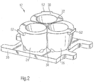
- a light curing device 10 has a light source 12 which, in the exemplary embodiment shown, comprises a plurality of semiconductor light sources. These include the three light-emitting chips 14, 16 and 18, which are mounted on a common substrate and the chip-cooling substrate 20.
- Each chip 14, 16 and 18 is surrounded by a reflector body, the chip 14 by the reflector body 22, the chip 16 by the reflector body 24 and the chip 18 by that Reflector body 26.
- the individual reflector bodies 22 to 26 are each carried by the substrate 20 and also fastened there.
- a gap is provided between the individual reflector bodies 22 to 26, namely the gap 30 between the reflector bodies 22 and 26, the gap 32 between the reflector bodies 22 and 24 and the gap 34 between the reflector bodies 24 and 26.
- This gap has a width according to the invention, which is selected such that even when the individual reflector bodies 22 to 26 are expanded, the relevant gaps 30 to 34 are not bridged, so that the reflector bodies 22 to 26 are always mechanically separated, without interfering in one system.
- the fastening of the individual reflector bodies 22 to 26 on the substrate 20 is chosen to be sufficiently dimensionally stable and firm that a system which would bridge the gaps does not arise due to vibrations or the like.
- each gap 30 to 34 in the cold state can have a size of, for example, 0.5 mm, it being understood that the required gap width is either calculated or can be determined by experiments.
- the reflector bodies 22 to 26 are made quite thick.
- the wall thickness of the reflector bodies can each be approximately 4 mm, with an adaptation to the requirements being possible over a wide range.
- the wall thickness of the reflector bodies for providing the gaps 30 to 34 in the adjacent regions of the reflector bodies 22 to 26 to each other is significantly reduced, especially in the upper region, that is to say in the region of the light exit surface 40 of the individual reflector bodies 22 to 26.
- the wall thickness can be, for example be reduced to the gap width or even to half the gap width, it being preferred according to the invention that the individual inner reflector surfaces are not intersected with one another.
- each reflector body 22 to 26 preferably has an inner surface 42 in the shape of a truncated parabola with a second opening also at the base, that is to say at the end of the reflector body 22, 24 and 26 on the substrate side, the thickness of the reflector body at the edge of this opening running out towards zero in the exemplary embodiment shown and the LED chips 14, 16 and 18 are each arranged in the focal point of the parabola inner surface 42.
- Assembly and repair can also be carried out in the case of an LED chip 14, 16 and 18 already connected to the substrate 20 through the opening in the base region of the reflector body 22, 24 and 26, the LED chip 14, 16 and 18 already before assembly of the reflector body 22, 24 and 26 brought into optimal thermal connection with the substrate 20 and this can be checked.
- the thermal resistance of the substrate 20 perpendicular to its surface is as low as possible; the substrate body can preferably consist essentially of a highly thermally conductive metal, such as copper or aluminum.
- the substrate body can preferably consist essentially of a highly thermally conductive metal, such as copper or aluminum.
- fluids in particular liquids, such as water or other cooling liquids or also gaseous air
- the light exit surfaces 40 or openings on the light exit side of the reflector bodies are preferred 22, 24 and 26 in one plane, as it is particularly characterized Fig. 2 is clearly visible.
- This plane can form a support surface 50 either for single converging lenses or for a common converging lens for the light source 12 or for a sophisticated optics which bundles the light emissions and focuses them as it is for the given application, namely the light curing of dental materials is cheap.
- a transparent cover plate and / or - depending on the application and field of application of the light curing device - a blocking filter for infrared and / or UV radiation and / or for other wavelength ranges can also be provided.
- a blocking filter for infrared and / or UV radiation and / or for other wavelength ranges can also be provided.
- the thermal separation between the converging lens and reflectors is also used and the deformation of the optics is prevented by heating the reflector bodies 22, 24 and 26.
- the light source 12 can be arranged both at the front end of a hand-held light curing device and in the base thereof, in the second case a light guide rod preferably extending in front of the light source 12.
- projections 52, 54 and 56 can preferably be provided, which can be formed on the outside / front of each individual reflector 22 to 26 and point outwards and in particular do not exceed the above-mentioned level.
- the reflector body 22, 24 and 26 is each comparatively cool after the heat is introduced primarily at the base of the reflector body 22, 24 and 26. The inclusion there is also possible without constructively demanding thermal insulation measures.
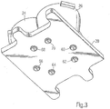
- the reflector bodies 22, 24 and 26 have depending downward projections 60, 62, 64, 66, 68 and 70, that is, each reflector body 22, 24, and 26 two each, which break through the substrate 20 and for a positive fit Ensure anchoring.
- the connecting line between two projections of a reflector body 22, 24 and 26, that is to say, for example, the projections 60 and 70 of the reflector body 26, is located below the relevant LED chip 14, 16 and 18 of the reflector, so that a symmetrical guidance is ensured in the event of thermal expansion of the substrate 20.
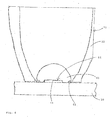
- Fig. 4 shows a sectional view through a reflector body 22 according to the exemplary embodiment described above, which additionally has a lens element 60 which is arranged directly above the LED chip 14.
- LED chips 14 emerging light radiation better, ie with a higher efficiency to the reflector of the reflector cone 22 and thereby increase the luminous efficiency, and on the other hand that portion of the radiation emerging from the surface 64 of the LED chip 14 pointing in the direction of radiation, which within the opening cone of the Reflector and thus would emerge without reflection at the reflector, are also fed to a focusing.
- Lens element 60 shown is preferably a liquid or plastic plastic mass of an optical plastic, such as polycarbonate, polymethyl methacrylate, cyclo-olefin (co) polymers or in particular silicone, applied in a viscous or plastic state to the substrate and above the LED chip 14 arranged on the substrate .
- This plastic compound surrounds the LED chip on its surface 64 pointing in the direction of radiation, as well as on the side surfaces, and spreads out to a ring 62 which is applied to the substrate and which differs in terms of its surface properties from that of the substrate 20 and which flows further the plastic mass stops, so that the plastic mass can form a hemisphere or spherical cap shape.
- the ring 62 in this exemplary embodiment is spaced on all sides both from the outer contours of the LED chip 14 and from the inner contour of the opening of the reflector cone 22.
- the ring 62 is produced here by a specific surface coating of the substrate, similar to a solder mask.
- a plastic or metal ring can be glued to the substrate surface, for example, the shape and / or surface properties of which limit the spread of the plastic compound.
- Chemical or physical surface treatment of the substrate surface is also possible, either in the form of a ring or in the form of a circular surface (in this case the circular surface would essentially have the size of the diameter of the plastic lens to be formed), which can likewise limit the spread of the applied plastic compound.
- this ring 62 it is possible to stop the spreading of the plastic compound on the inner circumference of the ring 62, or only on the outer circumference of the ring 62.
- the nature of the ring 62 can be chosen so that the spreading plastic mass only covers part of the ring width.
- the plastic mass applied connects on the one hand to the substrate 20, which simultaneously ensures a particularly good mechanical and thermal connection of the LED chip 14 to the substrate 20, and on the other hand to the chip surface, so that there - In particular with identical or similar refractive indices of the respective plastic of LED chip 14 and plastic mass - optical interface phenomena can be avoided or greatly reduced.
- this can be Fig. 4 also easily recognize the one-sided flattening 70 of the outer wall of the reflector cone 22, which would be located between two adjoining reflector cones 22 and which together forms the gap which enables the thermal expansion of the reflector cones 22 with the opposite flattened reflector wall 70 of the adjacent reflector cone 22.
- Fig. 5 shows an alternative embodiment of a reflector body 22 with a lens element 60 mounted on the LED chip 14.
- This embodiment does not require a ring 62 applied to the substrate 20, and instead uses the inner contour of the opening on the underside in the reflector cone 22 to limit the spread of the liquid or plastic plastic mass.
- Fig. 6 shows a third exemplary embodiment of a reflector body 22, which here is formed in two parts, consisting of ring or guide element 62 and reflector attachment 68, with a lens element 60 placed on the LED chip 14.
- the LED chip 14 is over a base element 66 connected to the substrate surface, for example a solder base, a heat-conducting base or another type of connection base, whereby the geometric and optical arrangement of the LED chip 14 within the reflector cone 22 and the mechanical anchoring of the LED chip 14 on the substrate 20 is improved and Heat dissipation is improved.
- a preferably metallic ring 62 is arranged around this base element 66, and at least partially in contact therewith, which can be positively positioned and centered by the base element 66.
- the ring 62 is provided here for the exact positioning of the reflector body 22, for which purpose the reflector body 22 has a groove in the bearing surface of the ring 62 on the substrate 20 which corresponds to the outer contour of the ring.
- this ring 62 simultaneously ensures a guiding function, by means of which a more precise positioning of the components and an improvement in the optical alignment can be achieved and at the same time the assembly can be simplified and made cheaper.
- the plastic drop extends up to the inner contour of the opening of the reflector body 22 on the substrate side.
Landscapes
- Health & Medical Sciences (AREA)
- Life Sciences & Earth Sciences (AREA)
- General Health & Medical Sciences (AREA)
- Oral & Maxillofacial Surgery (AREA)
- Dentistry (AREA)
- Epidemiology (AREA)
- Veterinary Medicine (AREA)
- Animal Behavior & Ethology (AREA)
- Public Health (AREA)
- General Engineering & Computer Science (AREA)
- Engineering & Computer Science (AREA)
- Led Device Packages (AREA)
- Non-Portable Lighting Devices Or Systems Thereof (AREA)
- Dental Tools And Instruments Or Auxiliary Dental Instruments (AREA)
- Arrangement Of Elements, Cooling, Sealing, Or The Like Of Lighting Devices (AREA)
Claims (15)
- Dispositif de photopolymérisation pour des applications dentaires, avec une pluralité de sources de lumière à semi-conducteurs, qui présentent chacune une puce émettrice de lumière (14 ; 16 et 18), où lesdites puces sont montées sur un substrat commun (20), où chaque puce (14, 16 et 18) est entourée par un seul corps réflecteur (22, 24 et 26) qui est relié au substrat (20), caractérisé en ce qu'au moins deux corps réflecteurs (22, 24 et 26) sont disposés côte à côte et séparés les uns des autres par une fente (30, 32 et 34) qui s'étend sur la même largeur par une ligne de séparation entre les corps réflecteurs adjacents (22, 24 et 26) de telle manière qu'ils sont découplés thermiquement et mécaniquement.
- Dispositif de photopolymérisation selon l'une des revendications précédentes, caractérisé en ce qu'au moins la surface de chaque puce émettrice de lumière (14, 16 et 18) orientée dans la direction d'émission est recouverte par une lentille respective (60) en matériau transparent et réfringent.
- Dispositif de photopolymérisation selon l'une des revendications précédentes, caractérisé en ce que la surface de la lentille (60) orientée dans la direction du rayonnement est essentiellement sphérique semi-sphérique.
- Dispositif de photopolymérisation selon l'une des revendications précédentes, caractérisé en ce que la puce émettrice de lumière (14, 16 et 18) repose par au moins deux de ses coins contre le corps réflecteur (22, 24 et 26) et détermine une position relative entre la puce et le corps réflecteur (22, 24 et 26).
- Dispositif de photopolymérisation selon l'une des revendications précédentes, caractérisé en ce que la lentille (60) s'étend jusqu'à une bague (62) appliqué sur le substrat (20), qui s'étend jusqu'à un contour intérieur du corps réflecteur (22, 24 et 26).
- Dispositif de photopolymérisation selon l'une des revendications précédentes, caractérisé en ce que la bague (62) est espacée de la puce émettrice de lumière (14, 16 et 18) en direction radiale.
- Dispositif de photopolymérisation selon l'une des revendications précédentes, caractérisé en ce que la lentille (60) recouvre au moins partiellement la surface de l'anneau (62) orientée dans la direction du rayonnement.
- Dispositif de photopolymérisation selon l'une des revendications précédentes, caractérisé en ce que la bague (62) est réalisé en tant que composant intégral du corps réflecteur (22, 24 et 26) ou en tant que composant supplémentaire d'un corps réflecteur (22, 24 et 26) au moins en deux parties, où les parties du corps de réflecteur (22, 24 et 26) constituées au moins de l'anneau (62) et de la fixation du réflecteur sont reliées entre elles mécaniquement et/ou matériellement.
- Dispositif de photopolymérisation selon l'une des revendications précédentes, caractérisé en ce que la bague (62) est conçue comme élément de guidage pour la puce émettrice de lumière (14, 16 et 18) et/ou comme élément de guidage pour le corps réflecteur (22, 24 et 26).
- Dispositif de photopolymérisation selon l'une des revendications précédentes, caractérisé en ce que les corps réflecteurs (22, 24 et 26) sont découplés au moins mécaniquement les uns des autres.
- un dispositif de photopolymérisation selon l'une des revendications précédentes, caractérisé en ce que les corps réflecteurs (22, 24 et 26) sont en liaison thermiquement conductrice avec le substrat (20), où les différents corps réflecteurs (22, 24 et 26) sont en contact étroit avec le substrat (20).
- dispositif de photopolymérisation selon l'une des revendications précédentes, caractérisé en ce que les puces émettrices de lumière (14, 16 et 18) sont couplées thermiquement au substrat (20).
- Dispositif de photopolymérisation selon l'une des revendications précédentes, caractérisé en ce que les corps réflecteurs (22, 24 et 26) présentent également une ouverture à l'extrémité située côté substrat qui est appropriée pour l'insertion d'une puce émettrice de lumière (14, 16 et 18) reliée au substrat (20).
- Dispositif de photopolymérisation selon l'une des revendications précédentes, caractérisé en ce que les surfaces périphériques extérieures se croisent dans la zone des faces frontales supérieures d'au moins deux corps réflecteurs (22, 24 et 26), où la fente formée entre deux corps réflecteurs définit une surface.
- Dispositif de photopolymérisation selon l'une des revendications précédentes, caractérisé en ce que les surfaces intérieures des réflecteurs adjacentes ne sont pas croisées entre elles.
Priority Applications (1)
| Application Number | Priority Date | Filing Date | Title |
|---|---|---|---|
| EP10194590.5A EP2332491B1 (fr) | 2009-12-10 | 2010-12-10 | Appareil de durcissement à la lumière à des fins dentaires |
Applications Claiming Priority (2)
| Application Number | Priority Date | Filing Date | Title |
|---|---|---|---|
| EP09178725.9A EP2332490B1 (fr) | 2009-12-10 | 2009-12-10 | Appareil de durcissement à la lumière à des fins dentaires |
| EP10194590.5A EP2332491B1 (fr) | 2009-12-10 | 2010-12-10 | Appareil de durcissement à la lumière à des fins dentaires |
Publications (2)
| Publication Number | Publication Date |
|---|---|
| EP2332491A1 EP2332491A1 (fr) | 2011-06-15 |
| EP2332491B1 true EP2332491B1 (fr) | 2020-05-27 |
Family
ID=42111725
Family Applications (2)
| Application Number | Title | Priority Date | Filing Date |
|---|---|---|---|
| EP09178725.9A Active EP2332490B1 (fr) | 2009-12-10 | 2009-12-10 | Appareil de durcissement à la lumière à des fins dentaires |
| EP10194590.5A Active EP2332491B1 (fr) | 2009-12-10 | 2010-12-10 | Appareil de durcissement à la lumière à des fins dentaires |
Family Applications Before (1)
| Application Number | Title | Priority Date | Filing Date |
|---|---|---|---|
| EP09178725.9A Active EP2332490B1 (fr) | 2009-12-10 | 2009-12-10 | Appareil de durcissement à la lumière à des fins dentaires |
Country Status (4)
| Country | Link |
|---|---|
| US (2) | US8632235B2 (fr) |
| EP (2) | EP2332490B1 (fr) |
| JP (1) | JP5480794B2 (fr) |
| ES (1) | ES2648041T3 (fr) |
Families Citing this family (10)
| Publication number | Priority date | Publication date | Assignee | Title |
|---|---|---|---|---|
| ES2648041T3 (es) * | 2009-12-10 | 2017-12-28 | Ivoclar Vivadent Ag | Dispositivo de fotopolimerización para finalidades dentales |
| KR101867284B1 (ko) * | 2011-07-01 | 2018-06-15 | 삼성전자주식회사 | 카메라 플래시 모듈 |
| PL395849A1 (pl) * | 2011-08-02 | 2013-02-04 | Automation 21 Llc. Christopher Slowinski | Zestaw oswietleniowy do mebli |
| AT513444B1 (de) * | 2012-10-09 | 2014-07-15 | Zizala Lichtsysteme Gmbh | Lichtmodul mit zwei oder mehr Reflektoren für ein Kraftfahrzeug sowie Kraftfahrzeugscheinwerfer |
| US10159548B2 (en) | 2014-09-17 | 2018-12-25 | Garrison Dental Solutions, L.L.C. | Dental curing light |
| EP3123976B1 (fr) * | 2015-07-31 | 2020-01-08 | Ivoclar Vivadent AG | Appareil de durcissement à la lumiere |
| TWM535782U (zh) * | 2016-09-22 | 2017-01-21 | 聯嘉光電股份有限公司 | 一種具有焦點定位之發光二極體陣列光杯結構 |
| USD810293S1 (en) | 2017-01-20 | 2018-02-13 | Garrison Dental Solutions, Llc | Dental instrument |
| DE202020100899U1 (de) * | 2020-02-19 | 2021-05-26 | Zumtobel Lighting Gmbh | Längliche Leuchte |
| US20240261075A1 (en) * | 2023-02-06 | 2024-08-08 | Prospedent LLC | Curing system and method |
Citations (2)
| Publication number | Priority date | Publication date | Assignee | Title |
|---|---|---|---|---|
| US7300175B2 (en) * | 2001-12-31 | 2007-11-27 | Innovations In Optics, Inc. | LED illuminator with retro reflector |
| EP2332490A1 (fr) * | 2009-12-10 | 2011-06-15 | Ivoclar Vivadent AG | Appareil de durcissement à la lumière à des fins dentaires |
Family Cites Families (25)
| Publication number | Priority date | Publication date | Assignee | Title |
|---|---|---|---|---|
| US1480904A (en) * | 1921-11-19 | 1924-01-15 | Gen Electric | Highway illuminator |
| US6200134B1 (en) | 1998-01-20 | 2001-03-13 | Kerr Corporation | Apparatus and method for curing materials with radiation |
| EP1031326A1 (fr) * | 1999-02-05 | 2000-08-30 | Jean-Michel Decaudin | Dispositif permettant la photo-activation de matériaux composites photosensibles utilisés notamment dans le domaine dentaire |
| US7320593B2 (en) * | 2000-03-08 | 2008-01-22 | Tir Systems Ltd. | Light emitting diode light source for curing dental composites |
| US6695614B2 (en) | 2001-02-01 | 2004-02-24 | Ivoclar Vivadent Ag | Light beam hardening apparatus for curing material |
| DE10104579B4 (de) | 2001-02-01 | 2004-02-19 | Ivoclar Vivadent Ag | Lichthärtgerät |
| US20020151941A1 (en) | 2001-04-16 | 2002-10-17 | Shinichi Okawa | Medical illuminator, and medical apparatus having the medical illuminator |
| JP2003190184A (ja) * | 2001-12-28 | 2003-07-08 | Morita Mfg Co Ltd | 医療用光重合器 |
| US6511317B2 (en) * | 2001-04-26 | 2003-01-28 | New Photonic, Llc | Device for curing photosensitive dental compositions with off-axis lens and method of curing |
| DE10125341B4 (de) | 2001-05-23 | 2006-11-23 | Ivoclar Vivadent Ag | Bestrahlungsvorrichtung und Lichthärtgerät |
| US7001057B2 (en) | 2001-05-23 | 2006-02-21 | Ivoclar Vivadent A.G. | Lighting apparatus for guiding light onto a light polymerizable piece to effect hardening thereof |
| DE10127416B4 (de) | 2001-06-06 | 2008-01-03 | Ivoclar Vivadent Ag | Lichthärtgerät sowie Lichtquelle mit einer Mehrzahl von LED's und einem Kühlkörper |
| US6767109B2 (en) | 2001-06-06 | 2004-07-27 | Ivoclar Vivadent Ag | Light hardening device and a light source suitable for use in a light hardening device |
| EP2009676B8 (fr) * | 2002-05-08 | 2012-11-21 | Phoseon Technology, Inc. | Systèmes d'inspection de matériaux à semi-conducteur |
| MXPA05001029A (es) * | 2002-07-25 | 2005-09-12 | Jonathan S Dahm | Metodo y aparato para utilizar diodos emisores de luz para curacion. |
| US7182597B2 (en) * | 2002-08-08 | 2007-02-27 | Kerr Corporation | Curing light instrument |
| AU2003298561A1 (en) * | 2002-08-23 | 2004-05-13 | Jonathan S. Dahm | Method and apparatus for using light emitting diodes |
| KR20050072152A (ko) * | 2002-12-02 | 2005-07-08 | 쓰리엠 이노베이티브 프로퍼티즈 컴파니 | 복수의 광원을 사용한 조사 시스템 |
| KR100643516B1 (ko) | 2003-05-06 | 2006-11-10 | 가부시키가이샤 모리타 세이사쿠쇼 | 의료용 광조사장치 |
| JP4056930B2 (ja) * | 2003-05-27 | 2008-03-05 | 株式会社モリタ製作所 | 医療用光照射装置 |
| DE102004007812A1 (de) | 2004-02-18 | 2005-09-22 | Adam Opel Ag | Scheinwerfer mit einem ellipsoidförmigen Reflektor |
| US7207694B1 (en) * | 2004-08-20 | 2007-04-24 | Boyd Industries, Inc. | Light emitting diode operating and examination light system |
| JP4744178B2 (ja) * | 2005-04-08 | 2011-08-10 | シャープ株式会社 | 発光ダイオード |
| US7906794B2 (en) | 2006-07-05 | 2011-03-15 | Koninklijke Philips Electronics N.V. | Light emitting device package with frame and optically transmissive element |
| US9086213B2 (en) * | 2007-10-17 | 2015-07-21 | Xicato, Inc. | Illumination device with light emitting diodes |
-
2009
- 2009-12-10 ES ES09178725.9T patent/ES2648041T3/es active Active
- 2009-12-10 EP EP09178725.9A patent/EP2332490B1/fr active Active
-
2010
- 2010-11-09 US US12/942,293 patent/US8632235B2/en active Active
- 2010-12-10 EP EP10194590.5A patent/EP2332491B1/fr active Active
- 2010-12-10 JP JP2010276451A patent/JP5480794B2/ja active Active
-
2013
- 2013-12-10 US US14/101,471 patent/US20140099596A1/en not_active Abandoned
Patent Citations (2)
| Publication number | Priority date | Publication date | Assignee | Title |
|---|---|---|---|---|
| US7300175B2 (en) * | 2001-12-31 | 2007-11-27 | Innovations In Optics, Inc. | LED illuminator with retro reflector |
| EP2332490A1 (fr) * | 2009-12-10 | 2011-06-15 | Ivoclar Vivadent AG | Appareil de durcissement à la lumière à des fins dentaires |
Also Published As
| Publication number | Publication date |
|---|---|
| US20110141733A1 (en) | 2011-06-16 |
| JP5480794B2 (ja) | 2014-04-23 |
| EP2332490B1 (fr) | 2017-10-11 |
| JP2011120914A (ja) | 2011-06-23 |
| US20140099596A1 (en) | 2014-04-10 |
| EP2332491A1 (fr) | 2011-06-15 |
| ES2648041T3 (es) | 2017-12-28 |
| EP2332490A1 (fr) | 2011-06-15 |
| US8632235B2 (en) | 2014-01-21 |
Similar Documents
| Publication | Publication Date | Title |
|---|---|---|
| EP2332491A1 (fr) | Appareil de durcissement à la lumière à des fins dentaires | |
| AT505107B1 (de) | Mikrolinsenarray, optisches modul und scheinwerfer | |
| DE102005030128B4 (de) | Lichtemittierende Vorrichtung und Beleuchtungsvorrichtung | |
| EP2614694B1 (fr) | Procédé pour recouvrir un module puce-sur-plaque optoélectronique d'un revêtement | |
| DE602004011186T2 (de) | Einheit zur Projektion eines Lichtbündels, eine optische Vorrichtung für die Einheit, und Fahrzeug Frontlichteinrichtung | |
| EP1467144B1 (fr) | Dispositif générateur de lumière avec réflecteur | |
| EP2459924B1 (fr) | Dispositif d'eclairage avec del | |
| EP2467635A1 (fr) | Lampe à led, en particulier phare à led | |
| WO2013056928A1 (fr) | Dispositif luminescent à semi-conducteur doté d'une lentille à structure photodéflectrice | |
| WO2006005393A2 (fr) | Spot a del pourvu d'une lentille en forme d'entonnoir | |
| DE102012223854A1 (de) | Remote-Phosphor-Konvertereinrichtung | |
| EP3321571B1 (fr) | Dispositif d'éclairage de salle d'opération mono-réflecteur | |
| WO2017102933A2 (fr) | Homogénéisateur à source de lumière | |
| DE102010046255A1 (de) | Beleuchtungsvorrichtung | |
| EP2494271B1 (fr) | Appareil d'éclairage destiné à éclairer une zone cible au moyen d'une réflexion arrière de lumière d'un module de diode électroluminescente sur un réflecteur | |
| DE202009014103U1 (de) | Leuchteinheit für eine Straßenlaterne | |
| DE112011101305B4 (de) | Lichtleitsystem, Verfahren zur Herstellung eines Lichtleitsystems und Anwendung eines Lichtleitsystems | |
| WO2004097293A1 (fr) | Support destine a une lampe et tete de lampe comportant un support et un reflecteur | |
| WO2008049381A1 (fr) | Dispositif d'éclairage | |
| DE102018109408A1 (de) | Led-modul mit silikonlinse in 3d druck | |
| WO2013117178A1 (fr) | Projecteur à réflecteur | |
| DE102016218139A1 (de) | Beleuchtungsvorrichtung | |
| EP2348250A1 (fr) | Lampe à DEL linéaire, notamment lampe annulaire à DEL | |
| DE19542985C2 (de) | Lichthärtgerät | |
| EP4015900B1 (fr) | Émetteur zoom |
Legal Events
| Date | Code | Title | Description |
|---|---|---|---|
| PUAI | Public reference made under article 153(3) epc to a published international application that has entered the european phase |
Free format text: ORIGINAL CODE: 0009012 |
|
| AK | Designated contracting states |
Kind code of ref document: A1 Designated state(s): AL AT BE BG CH CY CZ DE DK EE ES FI FR GB GR HR HU IE IS IT LI LT LU LV MC MK MT NL NO PL PT RO RS SE SI SK SM TR |
|
| AX | Request for extension of the european patent |
Extension state: BA ME |
|
| 17P | Request for examination filed |
Effective date: 20111028 |
|
| 17Q | First examination report despatched |
Effective date: 20140526 |
|
| STAA | Information on the status of an ep patent application or granted ep patent |
Free format text: STATUS: EXAMINATION IS IN PROGRESS |
|
| GRAP | Despatch of communication of intention to grant a patent |
Free format text: ORIGINAL CODE: EPIDOSNIGR1 |
|
| STAA | Information on the status of an ep patent application or granted ep patent |
Free format text: STATUS: GRANT OF PATENT IS INTENDED |
|
| INTG | Intention to grant announced |
Effective date: 20191216 |
|
| GRAS | Grant fee paid |
Free format text: ORIGINAL CODE: EPIDOSNIGR3 |
|
| GRAA | (expected) grant |
Free format text: ORIGINAL CODE: 0009210 |
|
| STAA | Information on the status of an ep patent application or granted ep patent |
Free format text: STATUS: THE PATENT HAS BEEN GRANTED |
|
| AK | Designated contracting states |
Kind code of ref document: B1 Designated state(s): AL AT BE BG CH CY CZ DE DK EE ES FI FR GB GR HR HU IE IS IT LI LT LU LV MC MK MT NL NO PL PT RO RS SE SI SK SM TR |
|
| REG | Reference to a national code |
Ref country code: GB Ref legal event code: FG4D Free format text: NOT ENGLISH |
|
| REG | Reference to a national code |
Ref country code: CH Ref legal event code: EP |
|
| REG | Reference to a national code |
Ref country code: DE Ref legal event code: R096 Ref document number: 502010016645 Country of ref document: DE |
|
| REG | Reference to a national code |
Ref country code: AT Ref legal event code: REF Ref document number: 1273731 Country of ref document: AT Kind code of ref document: T Effective date: 20200615 |
|
| REG | Reference to a national code |
Ref country code: CH Ref legal event code: NV Representative=s name: KELLER AND PARTNER PATENTANWAELTE AG, CH |
|
| REG | Reference to a national code |
Ref country code: CH Ref legal event code: PFA Owner name: IVOCLAR VIVADENT AG, LI Free format text: FORMER OWNER: IVOCLAR VIVADENT AG, LI |
|
| REG | Reference to a national code |
Ref country code: LT Ref legal event code: MG4D |
|
| PG25 | Lapsed in a contracting state [announced via postgrant information from national office to epo] |
Ref country code: PT Free format text: LAPSE BECAUSE OF FAILURE TO SUBMIT A TRANSLATION OF THE DESCRIPTION OR TO PAY THE FEE WITHIN THE PRESCRIBED TIME-LIMIT Effective date: 20200928 Ref country code: IS Free format text: LAPSE BECAUSE OF FAILURE TO SUBMIT A TRANSLATION OF THE DESCRIPTION OR TO PAY THE FEE WITHIN THE PRESCRIBED TIME-LIMIT Effective date: 20200927 Ref country code: SE Free format text: LAPSE BECAUSE OF FAILURE TO SUBMIT A TRANSLATION OF THE DESCRIPTION OR TO PAY THE FEE WITHIN THE PRESCRIBED TIME-LIMIT Effective date: 20200527 Ref country code: LT Free format text: LAPSE BECAUSE OF FAILURE TO SUBMIT A TRANSLATION OF THE DESCRIPTION OR TO PAY THE FEE WITHIN THE PRESCRIBED TIME-LIMIT Effective date: 20200527 Ref country code: GR Free format text: LAPSE BECAUSE OF FAILURE TO SUBMIT A TRANSLATION OF THE DESCRIPTION OR TO PAY THE FEE WITHIN THE PRESCRIBED TIME-LIMIT Effective date: 20200828 Ref country code: NO Free format text: LAPSE BECAUSE OF FAILURE TO SUBMIT A TRANSLATION OF THE DESCRIPTION OR TO PAY THE FEE WITHIN THE PRESCRIBED TIME-LIMIT Effective date: 20200827 Ref country code: FI Free format text: LAPSE BECAUSE OF FAILURE TO SUBMIT A TRANSLATION OF THE DESCRIPTION OR TO PAY THE FEE WITHIN THE PRESCRIBED TIME-LIMIT Effective date: 20200527 |
|
| REG | Reference to a national code |
Ref country code: NL Ref legal event code: MP Effective date: 20200527 |
|
| PG25 | Lapsed in a contracting state [announced via postgrant information from national office to epo] |
Ref country code: RS Free format text: LAPSE BECAUSE OF FAILURE TO SUBMIT A TRANSLATION OF THE DESCRIPTION OR TO PAY THE FEE WITHIN THE PRESCRIBED TIME-LIMIT Effective date: 20200527 Ref country code: BG Free format text: LAPSE BECAUSE OF FAILURE TO SUBMIT A TRANSLATION OF THE DESCRIPTION OR TO PAY THE FEE WITHIN THE PRESCRIBED TIME-LIMIT Effective date: 20200827 Ref country code: LV Free format text: LAPSE BECAUSE OF FAILURE TO SUBMIT A TRANSLATION OF THE DESCRIPTION OR TO PAY THE FEE WITHIN THE PRESCRIBED TIME-LIMIT Effective date: 20200527 Ref country code: HR Free format text: LAPSE BECAUSE OF FAILURE TO SUBMIT A TRANSLATION OF THE DESCRIPTION OR TO PAY THE FEE WITHIN THE PRESCRIBED TIME-LIMIT Effective date: 20200527 |
|
| PG25 | Lapsed in a contracting state [announced via postgrant information from national office to epo] |
Ref country code: NL Free format text: LAPSE BECAUSE OF FAILURE TO SUBMIT A TRANSLATION OF THE DESCRIPTION OR TO PAY THE FEE WITHIN THE PRESCRIBED TIME-LIMIT Effective date: 20200527 Ref country code: AL Free format text: LAPSE BECAUSE OF FAILURE TO SUBMIT A TRANSLATION OF THE DESCRIPTION OR TO PAY THE FEE WITHIN THE PRESCRIBED TIME-LIMIT Effective date: 20200527 |
|
| PG25 | Lapsed in a contracting state [announced via postgrant information from national office to epo] |
Ref country code: DK Free format text: LAPSE BECAUSE OF FAILURE TO SUBMIT A TRANSLATION OF THE DESCRIPTION OR TO PAY THE FEE WITHIN THE PRESCRIBED TIME-LIMIT Effective date: 20200527 Ref country code: SM Free format text: LAPSE BECAUSE OF FAILURE TO SUBMIT A TRANSLATION OF THE DESCRIPTION OR TO PAY THE FEE WITHIN THE PRESCRIBED TIME-LIMIT Effective date: 20200527 Ref country code: EE Free format text: LAPSE BECAUSE OF FAILURE TO SUBMIT A TRANSLATION OF THE DESCRIPTION OR TO PAY THE FEE WITHIN THE PRESCRIBED TIME-LIMIT Effective date: 20200527 Ref country code: RO Free format text: LAPSE BECAUSE OF FAILURE TO SUBMIT A TRANSLATION OF THE DESCRIPTION OR TO PAY THE FEE WITHIN THE PRESCRIBED TIME-LIMIT Effective date: 20200527 Ref country code: CZ Free format text: LAPSE BECAUSE OF FAILURE TO SUBMIT A TRANSLATION OF THE DESCRIPTION OR TO PAY THE FEE WITHIN THE PRESCRIBED TIME-LIMIT Effective date: 20200527 Ref country code: ES Free format text: LAPSE BECAUSE OF FAILURE TO SUBMIT A TRANSLATION OF THE DESCRIPTION OR TO PAY THE FEE WITHIN THE PRESCRIBED TIME-LIMIT Effective date: 20200527 |
|
| PG25 | Lapsed in a contracting state [announced via postgrant information from national office to epo] |
Ref country code: PL Free format text: LAPSE BECAUSE OF FAILURE TO SUBMIT A TRANSLATION OF THE DESCRIPTION OR TO PAY THE FEE WITHIN THE PRESCRIBED TIME-LIMIT Effective date: 20200527 Ref country code: SK Free format text: LAPSE BECAUSE OF FAILURE TO SUBMIT A TRANSLATION OF THE DESCRIPTION OR TO PAY THE FEE WITHIN THE PRESCRIBED TIME-LIMIT Effective date: 20200527 |
|
| REG | Reference to a national code |
Ref country code: DE Ref legal event code: R097 Ref document number: 502010016645 Country of ref document: DE |
|
| PLBE | No opposition filed within time limit |
Free format text: ORIGINAL CODE: 0009261 |
|
| STAA | Information on the status of an ep patent application or granted ep patent |
Free format text: STATUS: NO OPPOSITION FILED WITHIN TIME LIMIT |
|
| 26N | No opposition filed |
Effective date: 20210302 |
|
| PG25 | Lapsed in a contracting state [announced via postgrant information from national office to epo] |
Ref country code: SI Free format text: LAPSE BECAUSE OF FAILURE TO SUBMIT A TRANSLATION OF THE DESCRIPTION OR TO PAY THE FEE WITHIN THE PRESCRIBED TIME-LIMIT Effective date: 20200527 |
|
| PG25 | Lapsed in a contracting state [announced via postgrant information from national office to epo] |
Ref country code: MC Free format text: LAPSE BECAUSE OF FAILURE TO SUBMIT A TRANSLATION OF THE DESCRIPTION OR TO PAY THE FEE WITHIN THE PRESCRIBED TIME-LIMIT Effective date: 20200527 |
|
| REG | Reference to a national code |
Ref country code: BE Ref legal event code: MM Effective date: 20201231 |
|
| PG25 | Lapsed in a contracting state [announced via postgrant information from national office to epo] |
Ref country code: IE Free format text: LAPSE BECAUSE OF NON-PAYMENT OF DUE FEES Effective date: 20201210 Ref country code: LU Free format text: LAPSE BECAUSE OF NON-PAYMENT OF DUE FEES Effective date: 20201210 |
|
| PG25 | Lapsed in a contracting state [announced via postgrant information from national office to epo] |
Ref country code: TR Free format text: LAPSE BECAUSE OF FAILURE TO SUBMIT A TRANSLATION OF THE DESCRIPTION OR TO PAY THE FEE WITHIN THE PRESCRIBED TIME-LIMIT Effective date: 20200527 Ref country code: MT Free format text: LAPSE BECAUSE OF FAILURE TO SUBMIT A TRANSLATION OF THE DESCRIPTION OR TO PAY THE FEE WITHIN THE PRESCRIBED TIME-LIMIT Effective date: 20200527 Ref country code: CY Free format text: LAPSE BECAUSE OF FAILURE TO SUBMIT A TRANSLATION OF THE DESCRIPTION OR TO PAY THE FEE WITHIN THE PRESCRIBED TIME-LIMIT Effective date: 20200527 |
|
| PG25 | Lapsed in a contracting state [announced via postgrant information from national office to epo] |
Ref country code: MK Free format text: LAPSE BECAUSE OF FAILURE TO SUBMIT A TRANSLATION OF THE DESCRIPTION OR TO PAY THE FEE WITHIN THE PRESCRIBED TIME-LIMIT Effective date: 20200527 |
|
| PG25 | Lapsed in a contracting state [announced via postgrant information from national office to epo] |
Ref country code: BE Free format text: LAPSE BECAUSE OF NON-PAYMENT OF DUE FEES Effective date: 20201231 |
|
| P01 | Opt-out of the competence of the unified patent court (upc) registered |
Effective date: 20230607 |
|
| PGFP | Annual fee paid to national office [announced via postgrant information from national office to epo] |
Ref country code: GB Payment date: 20231107 Year of fee payment: 14 |
|
| PGFP | Annual fee paid to national office [announced via postgrant information from national office to epo] |
Ref country code: IT Payment date: 20231218 Year of fee payment: 14 Ref country code: FR Payment date: 20231107 Year of fee payment: 14 Ref country code: DE Payment date: 20231107 Year of fee payment: 14 Ref country code: AT Payment date: 20231114 Year of fee payment: 14 |
|
| PGFP | Annual fee paid to national office [announced via postgrant information from national office to epo] |
Ref country code: CH Payment date: 20240101 Year of fee payment: 14 |
|
| REG | Reference to a national code |
Ref country code: DE Ref legal event code: R119 Ref document number: 502010016645 Country of ref document: DE |
|
| REG | Reference to a national code |
Ref country code: CH Ref legal event code: PL |
|
| REG | Reference to a national code |
Ref country code: AT Ref legal event code: MM01 Ref document number: 1273731 Country of ref document: AT Kind code of ref document: T Effective date: 20241210 |
|
| GBPC | Gb: european patent ceased through non-payment of renewal fee |
Effective date: 20241210 |
|
| PG25 | Lapsed in a contracting state [announced via postgrant information from national office to epo] |
Ref country code: DE Free format text: LAPSE BECAUSE OF NON-PAYMENT OF DUE FEES Effective date: 20250701 |
|
| PG25 | Lapsed in a contracting state [announced via postgrant information from national office to epo] |
Ref country code: IT Free format text: LAPSE BECAUSE OF NON-PAYMENT OF DUE FEES Effective date: 20241210 |
|
| PG25 | Lapsed in a contracting state [announced via postgrant information from national office to epo] |
Ref country code: GB Free format text: LAPSE BECAUSE OF NON-PAYMENT OF DUE FEES Effective date: 20241210 |
|
| PG25 | Lapsed in a contracting state [announced via postgrant information from national office to epo] |
Ref country code: AT Free format text: LAPSE BECAUSE OF NON-PAYMENT OF DUE FEES Effective date: 20241210 Ref country code: FR Free format text: LAPSE BECAUSE OF NON-PAYMENT OF DUE FEES Effective date: 20241231 |
|
| PG25 | Lapsed in a contracting state [announced via postgrant information from national office to epo] |
Ref country code: CH Free format text: LAPSE BECAUSE OF NON-PAYMENT OF DUE FEES Effective date: 20241231 |