EP2333596A1 - Procédé de fabrication d'un guide d'ondes optiques - Google Patents
Procédé de fabrication d'un guide d'ondes optiques Download PDFInfo
- Publication number
- EP2333596A1 EP2333596A1 EP09809986A EP09809986A EP2333596A1 EP 2333596 A1 EP2333596 A1 EP 2333596A1 EP 09809986 A EP09809986 A EP 09809986A EP 09809986 A EP09809986 A EP 09809986A EP 2333596 A1 EP2333596 A1 EP 2333596A1
- Authority
- EP
- European Patent Office
- Prior art keywords
- optical waveguide
- core
- region
- manufacturing
- solution
- Prior art date
- Legal status (The legal status is an assumption and is not a legal conclusion. Google has not performed a legal analysis and makes no representation as to the accuracy of the status listed.)
- Withdrawn
Links
- 230000003287 optical effect Effects 0.000 title claims abstract description 152
- 238000000034 method Methods 0.000 title claims abstract description 57
- 238000004519 manufacturing process Methods 0.000 title claims abstract description 55
- 238000000576 coating method Methods 0.000 claims abstract description 133
- 239000011248 coating agent Substances 0.000 claims abstract description 131
- 238000010438 heat treatment Methods 0.000 claims abstract description 50
- 230000005855 radiation Effects 0.000 claims abstract description 46
- XUIMIQQOPSSXEZ-UHFFFAOYSA-N Silicon Chemical group [Si] XUIMIQQOPSSXEZ-UHFFFAOYSA-N 0.000 claims abstract description 33
- 229910052710 silicon Inorganic materials 0.000 claims abstract description 33
- 239000002243 precursor Substances 0.000 claims abstract description 30
- RTAQQCXQSZGOHL-UHFFFAOYSA-N Titanium Chemical group [Ti] RTAQQCXQSZGOHL-UHFFFAOYSA-N 0.000 claims abstract description 25
- 229910052719 titanium Inorganic materials 0.000 claims abstract description 25
- 230000001678 irradiating effect Effects 0.000 claims abstract description 12
- 238000006068 polycondensation reaction Methods 0.000 claims description 10
- 230000015572 biosynthetic process Effects 0.000 claims description 9
- 238000011049 filling Methods 0.000 claims description 6
- 230000005540 biological transmission Effects 0.000 claims description 4
- 239000000243 solution Substances 0.000 description 90
- 239000002904 solvent Substances 0.000 description 19
- 239000011347 resin Substances 0.000 description 16
- 229920005989 resin Polymers 0.000 description 16
- 239000000758 substrate Substances 0.000 description 16
- 229910052751 metal Inorganic materials 0.000 description 15
- 239000002184 metal Substances 0.000 description 15
- DNIAPMSPPWPWGF-UHFFFAOYSA-N Propylene glycol Chemical compound CC(O)CO DNIAPMSPPWPWGF-UHFFFAOYSA-N 0.000 description 13
- 150000004703 alkoxides Chemical class 0.000 description 12
- 239000013307 optical fiber Substances 0.000 description 11
- LYCAIKOWRPUZTN-UHFFFAOYSA-N Ethylene glycol Chemical compound OCCO LYCAIKOWRPUZTN-UHFFFAOYSA-N 0.000 description 10
- 238000009833 condensation Methods 0.000 description 10
- 230000005494 condensation Effects 0.000 description 10
- 239000000047 product Substances 0.000 description 10
- 239000003381 stabilizer Substances 0.000 description 10
- 230000007062 hydrolysis Effects 0.000 description 9
- 238000006460 hydrolysis reaction Methods 0.000 description 9
- 150000001875 compounds Chemical class 0.000 description 8
- 239000010703 silicon Substances 0.000 description 8
- 239000003054 catalyst Substances 0.000 description 7
- 238000001035 drying Methods 0.000 description 7
- VYPSYNLAJGMNEJ-UHFFFAOYSA-N Silicium dioxide Chemical compound O=[Si]=O VYPSYNLAJGMNEJ-UHFFFAOYSA-N 0.000 description 6
- -1 ethyacetylacetone Chemical compound 0.000 description 6
- 239000000463 material Substances 0.000 description 6
- 238000002360 preparation method Methods 0.000 description 6
- XLYOFNOQVPJJNP-UHFFFAOYSA-N water Substances O XLYOFNOQVPJJNP-UHFFFAOYSA-N 0.000 description 6
- 230000000694 effects Effects 0.000 description 5
- 229910001960 metal nitrate Inorganic materials 0.000 description 5
- 235000013772 propylene glycol Nutrition 0.000 description 5
- YNGDWRXWKFWCJY-UHFFFAOYSA-N 1,4-Dihydropyridine Chemical class C1C=CNC=C1 YNGDWRXWKFWCJY-UHFFFAOYSA-N 0.000 description 4
- XEEYBQQBJWHFJM-UHFFFAOYSA-N Iron Chemical compound [Fe] XEEYBQQBJWHFJM-UHFFFAOYSA-N 0.000 description 4
- BOTDANWDWHJENH-UHFFFAOYSA-N Tetraethyl orthosilicate Chemical compound CCO[Si](OCC)(OCC)OCC BOTDANWDWHJENH-UHFFFAOYSA-N 0.000 description 4
- 238000004891 communication Methods 0.000 description 4
- 230000008030 elimination Effects 0.000 description 4
- 238000003379 elimination reaction Methods 0.000 description 4
- 239000000835 fiber Substances 0.000 description 4
- 239000011521 glass Substances 0.000 description 4
- 150000002334 glycols Chemical class 0.000 description 4
- 239000011259 mixed solution Substances 0.000 description 4
- 125000004169 (C1-C6) alkyl group Chemical group 0.000 description 3
- ZWEHNKRNPOVVGH-UHFFFAOYSA-N 2-Butanone Chemical compound CCC(C)=O ZWEHNKRNPOVVGH-UHFFFAOYSA-N 0.000 description 3
- QTBSBXVTEAMEQO-UHFFFAOYSA-N Acetic acid Chemical compound CC(O)=O QTBSBXVTEAMEQO-UHFFFAOYSA-N 0.000 description 3
- UHOVQNZJYSORNB-UHFFFAOYSA-N Benzene Chemical compound C1=CC=CC=C1 UHOVQNZJYSORNB-UHFFFAOYSA-N 0.000 description 3
- OKKJLVBELUTLKV-UHFFFAOYSA-N Methanol Chemical compound OC OKKJLVBELUTLKV-UHFFFAOYSA-N 0.000 description 3
- ZMXDDKWLCZADIW-UHFFFAOYSA-N N,N-Dimethylformamide Chemical compound CN(C)C=O ZMXDDKWLCZADIW-UHFFFAOYSA-N 0.000 description 3
- MUBZPKHOEPUJKR-UHFFFAOYSA-N Oxalic acid Chemical compound OC(=O)C(O)=O MUBZPKHOEPUJKR-UHFFFAOYSA-N 0.000 description 3
- BQCADISMDOOEFD-UHFFFAOYSA-N Silver Chemical compound [Ag] BQCADISMDOOEFD-UHFFFAOYSA-N 0.000 description 3
- YXFVVABEGXRONW-UHFFFAOYSA-N Toluene Chemical compound CC1=CC=CC=C1 YXFVVABEGXRONW-UHFFFAOYSA-N 0.000 description 3
- 238000006243 chemical reaction Methods 0.000 description 3
- 229910052681 coesite Inorganic materials 0.000 description 3
- 238000013329 compounding Methods 0.000 description 3
- 229910052906 cristobalite Inorganic materials 0.000 description 3
- 230000000704 physical effect Effects 0.000 description 3
- 239000004033 plastic Substances 0.000 description 3
- 229920003023 plastic Polymers 0.000 description 3
- 230000008054 signal transmission Effects 0.000 description 3
- 239000000377 silicon dioxide Substances 0.000 description 3
- 229910052709 silver Inorganic materials 0.000 description 3
- 239000004332 silver Substances 0.000 description 3
- 238000004528 spin coating Methods 0.000 description 3
- 229910052682 stishovite Inorganic materials 0.000 description 3
- LFQCEHFDDXELDD-UHFFFAOYSA-N tetramethyl orthosilicate Chemical compound CO[Si](OC)(OC)OC LFQCEHFDDXELDD-UHFFFAOYSA-N 0.000 description 3
- 229910052905 tridymite Inorganic materials 0.000 description 3
- POAOYUHQDCAZBD-UHFFFAOYSA-N 2-butoxyethanol Chemical compound CCCCOCCO POAOYUHQDCAZBD-UHFFFAOYSA-N 0.000 description 2
- SVTBMSDMJJWYQN-UHFFFAOYSA-N 2-methylpentane-2,4-diol Chemical compound CC(O)CC(C)(C)O SVTBMSDMJJWYQN-UHFFFAOYSA-N 0.000 description 2
- NMUBRRLYMADSGF-UHFFFAOYSA-N 3-triethoxysilylpropan-1-ol Chemical compound CCO[Si](OCC)(OCC)CCCO NMUBRRLYMADSGF-UHFFFAOYSA-N 0.000 description 2
- YATIYDNBFHEOFA-UHFFFAOYSA-N 3-trimethoxysilylpropan-1-ol Chemical compound CO[Si](OC)(OC)CCCO YATIYDNBFHEOFA-UHFFFAOYSA-N 0.000 description 2
- CSCPPACGZOOCGX-UHFFFAOYSA-N Acetone Chemical compound CC(C)=O CSCPPACGZOOCGX-UHFFFAOYSA-N 0.000 description 2
- QGZKDVFQNNGYKY-UHFFFAOYSA-N Ammonia Chemical compound N QGZKDVFQNNGYKY-UHFFFAOYSA-N 0.000 description 2
- IJGRMHOSHXDMSA-UHFFFAOYSA-N Atomic nitrogen Chemical compound N#N IJGRMHOSHXDMSA-UHFFFAOYSA-N 0.000 description 2
- 229910052684 Cerium Inorganic materials 0.000 description 2
- VYZAMTAEIAYCRO-UHFFFAOYSA-N Chromium Chemical compound [Cr] VYZAMTAEIAYCRO-UHFFFAOYSA-N 0.000 description 2
- RYGMFSIKBFXOCR-UHFFFAOYSA-N Copper Chemical compound [Cu] RYGMFSIKBFXOCR-UHFFFAOYSA-N 0.000 description 2
- XTHFKEDIFFGKHM-UHFFFAOYSA-N Dimethoxyethane Chemical compound COCCOC XTHFKEDIFFGKHM-UHFFFAOYSA-N 0.000 description 2
- LFQSCWFLJHTTHZ-UHFFFAOYSA-N Ethanol Chemical compound CCO LFQSCWFLJHTTHZ-UHFFFAOYSA-N 0.000 description 2
- VEXZGXHMUGYJMC-UHFFFAOYSA-N Hydrochloric acid Chemical compound Cl VEXZGXHMUGYJMC-UHFFFAOYSA-N 0.000 description 2
- LRHPLDYGYMQRHN-UHFFFAOYSA-N N-Butanol Chemical compound CCCCO LRHPLDYGYMQRHN-UHFFFAOYSA-N 0.000 description 2
- KDLHZDBZIXYQEI-UHFFFAOYSA-N Palladium Chemical compound [Pd] KDLHZDBZIXYQEI-UHFFFAOYSA-N 0.000 description 2
- NBIIXXVUZAFLBC-UHFFFAOYSA-N Phosphoric acid Chemical compound OP(O)(O)=O NBIIXXVUZAFLBC-UHFFFAOYSA-N 0.000 description 2
- QAOWNCQODCNURD-UHFFFAOYSA-N Sulfuric acid Chemical compound OS(O)(=O)=O QAOWNCQODCNURD-UHFFFAOYSA-N 0.000 description 2
- YRKCREAYFQTBPV-UHFFFAOYSA-N acetylacetone Chemical compound CC(=O)CC(C)=O YRKCREAYFQTBPV-UHFFFAOYSA-N 0.000 description 2
- 229910052782 aluminium Inorganic materials 0.000 description 2
- XAGFODPZIPBFFR-UHFFFAOYSA-N aluminium Chemical compound [Al] XAGFODPZIPBFFR-UHFFFAOYSA-N 0.000 description 2
- 229910052797 bismuth Inorganic materials 0.000 description 2
- JCXGWMGPZLAOME-UHFFFAOYSA-N bismuth atom Chemical compound [Bi] JCXGWMGPZLAOME-UHFFFAOYSA-N 0.000 description 2
- 229910052793 cadmium Inorganic materials 0.000 description 2
- BDOSMKKIYDKNTQ-UHFFFAOYSA-N cadmium atom Chemical compound [Cd] BDOSMKKIYDKNTQ-UHFFFAOYSA-N 0.000 description 2
- 239000000919 ceramic Substances 0.000 description 2
- ZMIGMASIKSOYAM-UHFFFAOYSA-N cerium Chemical compound [Ce][Ce][Ce][Ce][Ce][Ce][Ce][Ce][Ce][Ce][Ce][Ce][Ce][Ce][Ce][Ce][Ce][Ce][Ce][Ce][Ce][Ce][Ce][Ce][Ce][Ce][Ce][Ce][Ce][Ce][Ce][Ce][Ce][Ce][Ce][Ce][Ce][Ce] ZMIGMASIKSOYAM-UHFFFAOYSA-N 0.000 description 2
- 239000003795 chemical substances by application Substances 0.000 description 2
- 229910052804 chromium Inorganic materials 0.000 description 2
- 239000011651 chromium Substances 0.000 description 2
- 229910017052 cobalt Inorganic materials 0.000 description 2
- 239000010941 cobalt Substances 0.000 description 2
- GUTLYIVDDKVIGB-UHFFFAOYSA-N cobalt atom Chemical compound [Co] GUTLYIVDDKVIGB-UHFFFAOYSA-N 0.000 description 2
- 239000007859 condensation product Substances 0.000 description 2
- 238000006482 condensation reaction Methods 0.000 description 2
- 238000011109 contamination Methods 0.000 description 2
- 229910052802 copper Inorganic materials 0.000 description 2
- 239000010949 copper Substances 0.000 description 2
- 238000000354 decomposition reaction Methods 0.000 description 2
- 230000007547 defect Effects 0.000 description 2
- XGZNHFPFJRZBBT-UHFFFAOYSA-N ethanol;titanium Chemical compound [Ti].CCO.CCO.CCO.CCO XGZNHFPFJRZBBT-UHFFFAOYSA-N 0.000 description 2
- FWDBOZPQNFPOLF-UHFFFAOYSA-N ethenyl(triethoxy)silane Chemical compound CCO[Si](OCC)(OCC)C=C FWDBOZPQNFPOLF-UHFFFAOYSA-N 0.000 description 2
- NKSJNEHGWDZZQF-UHFFFAOYSA-N ethenyl(trimethoxy)silane Chemical compound CO[Si](OC)(OC)C=C NKSJNEHGWDZZQF-UHFFFAOYSA-N 0.000 description 2
- 238000011156 evaluation Methods 0.000 description 2
- 229910052738 indium Inorganic materials 0.000 description 2
- APFVFJFRJDLVQX-UHFFFAOYSA-N indium atom Chemical compound [In] APFVFJFRJDLVQX-UHFFFAOYSA-N 0.000 description 2
- 229910052742 iron Inorganic materials 0.000 description 2
- WPBNNNQJVZRUHP-UHFFFAOYSA-L manganese(2+);methyl n-[[2-(methoxycarbonylcarbamothioylamino)phenyl]carbamothioyl]carbamate;n-[2-(sulfidocarbothioylamino)ethyl]carbamodithioate Chemical compound [Mn+2].[S-]C(=S)NCCNC([S-])=S.COC(=O)NC(=S)NC1=CC=CC=C1NC(=S)NC(=O)OC WPBNNNQJVZRUHP-UHFFFAOYSA-L 0.000 description 2
- 229910001507 metal halide Inorganic materials 0.000 description 2
- 150000005309 metal halides Chemical class 0.000 description 2
- BDAGIHXWWSANSR-UHFFFAOYSA-N methanoic acid Natural products OC=O BDAGIHXWWSANSR-UHFFFAOYSA-N 0.000 description 2
- BFXIKLCIZHOAAZ-UHFFFAOYSA-N methyltrimethoxysilane Chemical compound CO[Si](C)(OC)OC BFXIKLCIZHOAAZ-UHFFFAOYSA-N 0.000 description 2
- 239000000203 mixture Substances 0.000 description 2
- 238000006116 polymerization reaction Methods 0.000 description 2
- 238000012545 processing Methods 0.000 description 2
- RLJWTAURUFQFJP-UHFFFAOYSA-N propan-2-ol;titanium Chemical compound [Ti].CC(C)O.CC(C)O.CC(C)O.CC(C)O RLJWTAURUFQFJP-UHFFFAOYSA-N 0.000 description 2
- 229910052723 transition metal Inorganic materials 0.000 description 2
- ZLGWXNBXAXOQBG-UHFFFAOYSA-N triethoxy(3,3,3-trifluoropropyl)silane Chemical compound CCO[Si](OCC)(OCC)CCC(F)(F)F ZLGWXNBXAXOQBG-UHFFFAOYSA-N 0.000 description 2
- CPUDPFPXCZDNGI-UHFFFAOYSA-N triethoxy(methyl)silane Chemical compound CCO[Si](C)(OCC)OCC CPUDPFPXCZDNGI-UHFFFAOYSA-N 0.000 description 2
- JCVQKRGIASEUKR-UHFFFAOYSA-N triethoxy(phenyl)silane Chemical compound CCO[Si](OCC)(OCC)C1=CC=CC=C1 JCVQKRGIASEUKR-UHFFFAOYSA-N 0.000 description 2
- JLGNHOJUQFHYEZ-UHFFFAOYSA-N trimethoxy(3,3,3-trifluoropropyl)silane Chemical compound CO[Si](OC)(OC)CCC(F)(F)F JLGNHOJUQFHYEZ-UHFFFAOYSA-N 0.000 description 2
- ZNOCGWVLWPVKAO-UHFFFAOYSA-N trimethoxy(phenyl)silane Chemical compound CO[Si](OC)(OC)C1=CC=CC=C1 ZNOCGWVLWPVKAO-UHFFFAOYSA-N 0.000 description 2
- BPSIOYPQMFLKFR-UHFFFAOYSA-N trimethoxy-[3-(oxiran-2-ylmethoxy)propyl]silane Chemical compound CO[Si](OC)(OC)CCCOCC1CO1 BPSIOYPQMFLKFR-UHFFFAOYSA-N 0.000 description 2
- WFKWXMTUELFFGS-UHFFFAOYSA-N tungsten Chemical compound [W] WFKWXMTUELFFGS-UHFFFAOYSA-N 0.000 description 2
- 229910052721 tungsten Inorganic materials 0.000 description 2
- 239000010937 tungsten Substances 0.000 description 2
- 229910052727 yttrium Inorganic materials 0.000 description 2
- VWQVUPCCIRVNHF-UHFFFAOYSA-N yttrium atom Chemical compound [Y] VWQVUPCCIRVNHF-UHFFFAOYSA-N 0.000 description 2
- 125000006727 (C1-C6) alkenyl group Chemical group 0.000 description 1
- DNIAPMSPPWPWGF-GSVOUGTGSA-N (R)-(-)-Propylene glycol Chemical compound C[C@@H](O)CO DNIAPMSPPWPWGF-GSVOUGTGSA-N 0.000 description 1
- LZDKZFUFMNSQCJ-UHFFFAOYSA-N 1,2-diethoxyethane Chemical compound CCOCCOCC LZDKZFUFMNSQCJ-UHFFFAOYSA-N 0.000 description 1
- RRQYJINTUHWNHW-UHFFFAOYSA-N 1-ethoxy-2-(2-ethoxyethoxy)ethane Chemical compound CCOCCOCCOCC RRQYJINTUHWNHW-UHFFFAOYSA-N 0.000 description 1
- OAYXUHPQHDHDDZ-UHFFFAOYSA-N 2-(2-butoxyethoxy)ethanol Chemical compound CCCCOCCOCCO OAYXUHPQHDHDDZ-UHFFFAOYSA-N 0.000 description 1
- XNWFRZJHXBZDAG-UHFFFAOYSA-N 2-METHOXYETHANOL Chemical compound COCCO XNWFRZJHXBZDAG-UHFFFAOYSA-N 0.000 description 1
- ZNQVEEAIQZEUHB-UHFFFAOYSA-N 2-ethoxyethanol Chemical compound CCOCCO ZNQVEEAIQZEUHB-UHFFFAOYSA-N 0.000 description 1
- KSCAZPYHLGGNPZ-UHFFFAOYSA-N 3-chloropropyl(triethoxy)silane Chemical compound CCO[Si](OCC)(OCC)CCCCl KSCAZPYHLGGNPZ-UHFFFAOYSA-N 0.000 description 1
- OXYZDRAJMHGSMW-UHFFFAOYSA-N 3-chloropropyl(trimethoxy)silane Chemical compound CO[Si](OC)(OC)CCCCl OXYZDRAJMHGSMW-UHFFFAOYSA-N 0.000 description 1
- GSOHKPVFCOWKPU-UHFFFAOYSA-N 3-methylpentane-2,4-dione Chemical compound CC(=O)C(C)C(C)=O GSOHKPVFCOWKPU-UHFFFAOYSA-N 0.000 description 1
- OSWFIVFLDKOXQC-UHFFFAOYSA-N 4-(3-methoxyphenyl)aniline Chemical compound COC1=CC=CC(C=2C=CC(N)=CC=2)=C1 OSWFIVFLDKOXQC-UHFFFAOYSA-N 0.000 description 1
- WTOINXDHRHCLLI-UHFFFAOYSA-N 5-ethylheptane-2,4-dione Chemical compound CCC(CC)C(=O)CC(C)=O WTOINXDHRHCLLI-UHFFFAOYSA-N 0.000 description 1
- 229920002284 Cellulose triacetate Polymers 0.000 description 1
- FYYHWMGAXLPEAU-UHFFFAOYSA-N Magnesium Chemical compound [Mg] FYYHWMGAXLPEAU-UHFFFAOYSA-N 0.000 description 1
- ZOKXTWBITQBERF-UHFFFAOYSA-N Molybdenum Chemical compound [Mo] ZOKXTWBITQBERF-UHFFFAOYSA-N 0.000 description 1
- SECXISVLQFMRJM-UHFFFAOYSA-N N-Methylpyrrolidone Chemical compound CN1CCCC1=O SECXISVLQFMRJM-UHFFFAOYSA-N 0.000 description 1
- 229910002651 NO3 Inorganic materials 0.000 description 1
- NHNBFGGVMKEFGY-UHFFFAOYSA-N Nitrate Chemical compound [O-][N+]([O-])=O NHNBFGGVMKEFGY-UHFFFAOYSA-N 0.000 description 1
- GRYLNZFGIOXLOG-UHFFFAOYSA-N Nitric acid Chemical compound O[N+]([O-])=O GRYLNZFGIOXLOG-UHFFFAOYSA-N 0.000 description 1
- CTQNGGLPUBDAKN-UHFFFAOYSA-N O-Xylene Chemical compound CC1=CC=CC=C1C CTQNGGLPUBDAKN-UHFFFAOYSA-N 0.000 description 1
- 239000004695 Polyether sulfone Substances 0.000 description 1
- 239000004642 Polyimide Substances 0.000 description 1
- 239000004721 Polyphenylene oxide Substances 0.000 description 1
- OFOBLEOULBTSOW-UHFFFAOYSA-N Propanedioic acid Natural products OC(=O)CC(O)=O OFOBLEOULBTSOW-UHFFFAOYSA-N 0.000 description 1
- NNLVGZFZQQXQNW-ADJNRHBOSA-N [(2r,3r,4s,5r,6s)-4,5-diacetyloxy-3-[(2s,3r,4s,5r,6r)-3,4,5-triacetyloxy-6-(acetyloxymethyl)oxan-2-yl]oxy-6-[(2r,3r,4s,5r,6s)-4,5,6-triacetyloxy-2-(acetyloxymethyl)oxan-3-yl]oxyoxan-2-yl]methyl acetate Chemical compound O([C@@H]1O[C@@H]([C@H]([C@H](OC(C)=O)[C@H]1OC(C)=O)O[C@H]1[C@@H]([C@@H](OC(C)=O)[C@H](OC(C)=O)[C@@H](COC(C)=O)O1)OC(C)=O)COC(=O)C)[C@@H]1[C@@H](COC(C)=O)O[C@@H](OC(C)=O)[C@H](OC(C)=O)[C@H]1OC(C)=O NNLVGZFZQQXQNW-ADJNRHBOSA-N 0.000 description 1
- 235000011054 acetic acid Nutrition 0.000 description 1
- UGZICOVULPINFH-UHFFFAOYSA-N acetic acid;butanoic acid Chemical compound CC(O)=O.CCCC(O)=O UGZICOVULPINFH-UHFFFAOYSA-N 0.000 description 1
- 239000002253 acid Substances 0.000 description 1
- 150000007513 acids Chemical class 0.000 description 1
- 150000001298 alcohols Chemical class 0.000 description 1
- 229910000147 aluminium phosphate Inorganic materials 0.000 description 1
- SWCIQHXIXUMHKA-UHFFFAOYSA-N aluminum;trinitrate;nonahydrate Chemical compound O.O.O.O.O.O.O.O.O.[Al+3].[O-][N+]([O-])=O.[O-][N+]([O-])=O.[O-][N+]([O-])=O SWCIQHXIXUMHKA-UHFFFAOYSA-N 0.000 description 1
- 229910021529 ammonia Inorganic materials 0.000 description 1
- 150000004945 aromatic hydrocarbons Chemical class 0.000 description 1
- 125000003118 aryl group Chemical group 0.000 description 1
- 239000012298 atmosphere Substances 0.000 description 1
- 229910052788 barium Inorganic materials 0.000 description 1
- DSAJWYNOEDNPEQ-UHFFFAOYSA-N barium atom Chemical compound [Ba] DSAJWYNOEDNPEQ-UHFFFAOYSA-N 0.000 description 1
- FPCJKVGGYOAWIZ-UHFFFAOYSA-N butan-1-ol;titanium Chemical compound [Ti].CCCCO.CCCCO.CCCCO.CCCCO FPCJKVGGYOAWIZ-UHFFFAOYSA-N 0.000 description 1
- XGZGKDQVCBHSGI-UHFFFAOYSA-N butyl(triethoxy)silane Chemical compound CCCC[Si](OCC)(OCC)OCC XGZGKDQVCBHSGI-UHFFFAOYSA-N 0.000 description 1
- SXPLZNMUBFBFIA-UHFFFAOYSA-N butyl(trimethoxy)silane Chemical compound CCCC[Si](OC)(OC)OC SXPLZNMUBFBFIA-UHFFFAOYSA-N 0.000 description 1
- 239000001913 cellulose Substances 0.000 description 1
- 229920002678 cellulose Polymers 0.000 description 1
- 239000002131 composite material Substances 0.000 description 1
- 238000001816 cooling Methods 0.000 description 1
- 238000011161 development Methods 0.000 description 1
- 229920005994 diacetyl cellulose Polymers 0.000 description 1
- XXJWXESWEXIICW-UHFFFAOYSA-N diethylene glycol monoethyl ether Chemical compound CCOCCOCCO XXJWXESWEXIICW-UHFFFAOYSA-N 0.000 description 1
- JJQZDUKDJDQPMQ-UHFFFAOYSA-N dimethoxy(dimethyl)silane Chemical compound CO[Si](C)(C)OC JJQZDUKDJDQPMQ-UHFFFAOYSA-N 0.000 description 1
- YYLGKUPAFFKGRQ-UHFFFAOYSA-N dimethyldiethoxysilane Chemical compound CCO[Si](C)(C)OCC YYLGKUPAFFKGRQ-UHFFFAOYSA-N 0.000 description 1
- 238000007598 dipping method Methods 0.000 description 1
- 238000009826 distribution Methods 0.000 description 1
- 238000009429 electrical wiring Methods 0.000 description 1
- 238000010894 electron beam technology Methods 0.000 description 1
- 230000002708 enhancing effect Effects 0.000 description 1
- SBRXLTRZCJVAPH-UHFFFAOYSA-N ethyl(trimethoxy)silane Chemical compound CC[Si](OC)(OC)OC SBRXLTRZCJVAPH-UHFFFAOYSA-N 0.000 description 1
- 235000019253 formic acid Nutrition 0.000 description 1
- VRINOTYEGADLMW-UHFFFAOYSA-N heptyl(trimethoxy)silane Chemical compound CCCCCCC[Si](OC)(OC)OC VRINOTYEGADLMW-UHFFFAOYSA-N 0.000 description 1
- CZWLNMOIEMTDJY-UHFFFAOYSA-N hexyl(trimethoxy)silane Chemical compound CCCCCC[Si](OC)(OC)OC CZWLNMOIEMTDJY-UHFFFAOYSA-N 0.000 description 1
- 229940051250 hexylene glycol Drugs 0.000 description 1
- 239000012456 homogeneous solution Substances 0.000 description 1
- 239000000413 hydrolysate Substances 0.000 description 1
- WGCNASOHLSPBMP-UHFFFAOYSA-N hydroxyacetaldehyde Natural products OCC=O WGCNASOHLSPBMP-UHFFFAOYSA-N 0.000 description 1
- 239000011261 inert gas Substances 0.000 description 1
- 239000010954 inorganic particle Substances 0.000 description 1
- 230000010354 integration Effects 0.000 description 1
- 150000002576 ketones Chemical class 0.000 description 1
- 229910052749 magnesium Inorganic materials 0.000 description 1
- 239000011777 magnesium Substances 0.000 description 1
- VZCYOOQTPOCHFL-UPHRSURJSA-N maleic acid Chemical compound OC(=O)\C=C/C(O)=O VZCYOOQTPOCHFL-UPHRSURJSA-N 0.000 description 1
- 239000011976 maleic acid Substances 0.000 description 1
- 238000005259 measurement Methods 0.000 description 1
- QSHDDOUJBYECFT-UHFFFAOYSA-N mercury Chemical compound [Hg] QSHDDOUJBYECFT-UHFFFAOYSA-N 0.000 description 1
- 229910052753 mercury Inorganic materials 0.000 description 1
- 150000002739 metals Chemical class 0.000 description 1
- ZEIWWVGGEOHESL-UHFFFAOYSA-N methanol;titanium Chemical compound [Ti].OC.OC.OC.OC ZEIWWVGGEOHESL-UHFFFAOYSA-N 0.000 description 1
- 229910052750 molybdenum Inorganic materials 0.000 description 1
- 239000011733 molybdenum Substances 0.000 description 1
- 239000000178 monomer Substances 0.000 description 1
- 229910052758 niobium Inorganic materials 0.000 description 1
- 239000010955 niobium Substances 0.000 description 1
- GUCVJGMIXFAOAE-UHFFFAOYSA-N niobium atom Chemical compound [Nb] GUCVJGMIXFAOAE-UHFFFAOYSA-N 0.000 description 1
- 150000002823 nitrates Chemical class 0.000 description 1
- 229910017604 nitric acid Inorganic materials 0.000 description 1
- 229910052757 nitrogen Inorganic materials 0.000 description 1
- SLYCYWCVSGPDFR-UHFFFAOYSA-N octadecyltrimethoxysilane Chemical compound CCCCCCCCCCCCCCCCCC[Si](OC)(OC)OC SLYCYWCVSGPDFR-UHFFFAOYSA-N 0.000 description 1
- MSRJTTSHWYDFIU-UHFFFAOYSA-N octyltriethoxysilane Chemical compound CCCCCCCC[Si](OCC)(OCC)OCC MSRJTTSHWYDFIU-UHFFFAOYSA-N 0.000 description 1
- 229960003493 octyltriethoxysilane Drugs 0.000 description 1
- 235000006408 oxalic acid Nutrition 0.000 description 1
- 238000012856 packing Methods 0.000 description 1
- 229910052763 palladium Inorganic materials 0.000 description 1
- 230000000737 periodic effect Effects 0.000 description 1
- 235000011007 phosphoric acid Nutrition 0.000 description 1
- 229920001643 poly(ether ketone) Polymers 0.000 description 1
- 229920002492 poly(sulfone) Polymers 0.000 description 1
- 229920000058 polyacrylate Polymers 0.000 description 1
- 229920000515 polycarbonate Polymers 0.000 description 1
- 239000004417 polycarbonate Substances 0.000 description 1
- 229920000570 polyether Polymers 0.000 description 1
- 229920006393 polyether sulfone Polymers 0.000 description 1
- 229920000139 polyethylene terephthalate Polymers 0.000 description 1
- 239000005020 polyethylene terephthalate Substances 0.000 description 1
- 229920001721 polyimide Polymers 0.000 description 1
- 229920000193 polymethacrylate Polymers 0.000 description 1
- 229920000098 polyolefin Polymers 0.000 description 1
- 229920002635 polyurethane Polymers 0.000 description 1
- 239000004814 polyurethane Substances 0.000 description 1
- 238000007639 printing Methods 0.000 description 1
- BDERNNFJNOPAEC-UHFFFAOYSA-N propan-1-ol Chemical compound CCCO BDERNNFJNOPAEC-UHFFFAOYSA-N 0.000 description 1
- 239000013557 residual solvent Substances 0.000 description 1
- 239000004065 semiconductor Substances 0.000 description 1
- 238000005507 spraying Methods 0.000 description 1
- 230000000087 stabilizing effect Effects 0.000 description 1
- 239000000126 substance Substances 0.000 description 1
- 239000004094 surface-active agent Substances 0.000 description 1
- 229910052715 tantalum Inorganic materials 0.000 description 1
- GUVRBAGPIYLISA-UHFFFAOYSA-N tantalum atom Chemical compound [Ta] GUVRBAGPIYLISA-UHFFFAOYSA-N 0.000 description 1
- UQMOLLPKNHFRAC-UHFFFAOYSA-N tetrabutyl silicate Chemical compound CCCCO[Si](OCCCC)(OCCCC)OCCCC UQMOLLPKNHFRAC-UHFFFAOYSA-N 0.000 description 1
- ZQZCOBSUOFHDEE-UHFFFAOYSA-N tetrapropyl silicate Chemical compound CCCO[Si](OCCC)(OCCC)OCCC ZQZCOBSUOFHDEE-UHFFFAOYSA-N 0.000 description 1
- 239000010936 titanium Substances 0.000 description 1
- VZCYOOQTPOCHFL-UHFFFAOYSA-N trans-butenedioic acid Natural products OC(=O)C=CC(O)=O VZCYOOQTPOCHFL-UHFFFAOYSA-N 0.000 description 1
- DENFJSAFJTVPJR-UHFFFAOYSA-N triethoxy(ethyl)silane Chemical compound CCO[Si](CC)(OCC)OCC DENFJSAFJTVPJR-UHFFFAOYSA-N 0.000 description 1
- SAWDTKLQESXBDN-UHFFFAOYSA-N triethoxy(heptyl)silane Chemical compound CCCCCCC[Si](OCC)(OCC)OCC SAWDTKLQESXBDN-UHFFFAOYSA-N 0.000 description 1
- WUMSTCDLAYQDNO-UHFFFAOYSA-N triethoxy(hexyl)silane Chemical compound CCCCCC[Si](OCC)(OCC)OCC WUMSTCDLAYQDNO-UHFFFAOYSA-N 0.000 description 1
- FZMJEGJVKFTGMU-UHFFFAOYSA-N triethoxy(octadecyl)silane Chemical compound CCCCCCCCCCCCCCCCCC[Si](OCC)(OCC)OCC FZMJEGJVKFTGMU-UHFFFAOYSA-N 0.000 description 1
- FHVAUDREWWXPRW-UHFFFAOYSA-N triethoxy(pentyl)silane Chemical compound CCCCC[Si](OCC)(OCC)OCC FHVAUDREWWXPRW-UHFFFAOYSA-N 0.000 description 1
- NBXZNTLFQLUFES-UHFFFAOYSA-N triethoxy(propyl)silane Chemical compound CCC[Si](OCC)(OCC)OCC NBXZNTLFQLUFES-UHFFFAOYSA-N 0.000 description 1
- NMEPHPOFYLLFTK-UHFFFAOYSA-N trimethoxy(octyl)silane Chemical compound CCCCCCCC[Si](OC)(OC)OC NMEPHPOFYLLFTK-UHFFFAOYSA-N 0.000 description 1
- HILHCDFHSDUYNX-UHFFFAOYSA-N trimethoxy(pentyl)silane Chemical compound CCCCC[Si](OC)(OC)OC HILHCDFHSDUYNX-UHFFFAOYSA-N 0.000 description 1
- HQYALQRYBUJWDH-UHFFFAOYSA-N trimethoxy(propyl)silane Chemical compound CCC[Si](OC)(OC)OC HQYALQRYBUJWDH-UHFFFAOYSA-N 0.000 description 1
- 230000005641 tunneling Effects 0.000 description 1
- 229910052724 xenon Inorganic materials 0.000 description 1
- FHNFHKCVQCLJFQ-UHFFFAOYSA-N xenon atom Chemical compound [Xe] FHNFHKCVQCLJFQ-UHFFFAOYSA-N 0.000 description 1
- 239000008096 xylene Substances 0.000 description 1
Images
Classifications
-
- G—PHYSICS
- G02—OPTICS
- G02B—OPTICAL ELEMENTS, SYSTEMS OR APPARATUS
- G02B6/00—Light guides; Structural details of arrangements comprising light guides and other optical elements, e.g. couplings
- G02B6/10—Light guides; Structural details of arrangements comprising light guides and other optical elements, e.g. couplings of the optical waveguide type
- G02B6/12—Light guides; Structural details of arrangements comprising light guides and other optical elements, e.g. couplings of the optical waveguide type of the integrated circuit kind
- G02B6/13—Integrated optical circuits characterised by the manufacturing method
- G02B6/138—Integrated optical circuits characterised by the manufacturing method by using polymerisation
-
- B—PERFORMING OPERATIONS; TRANSPORTING
- B82—NANOTECHNOLOGY
- B82Y—SPECIFIC USES OR APPLICATIONS OF NANOSTRUCTURES; MEASUREMENT OR ANALYSIS OF NANOSTRUCTURES; MANUFACTURE OR TREATMENT OF NANOSTRUCTURES
- B82Y20/00—Nanooptics, e.g. quantum optics or photonic crystals
-
- G—PHYSICS
- G02—OPTICS
- G02B—OPTICAL ELEMENTS, SYSTEMS OR APPARATUS
- G02B1/00—Optical elements characterised by the material of which they are made; Optical coatings for optical elements
- G02B1/04—Optical elements characterised by the material of which they are made; Optical coatings for optical elements made of organic materials, e.g. plastics
- G02B1/045—Light guides
-
- G—PHYSICS
- G02—OPTICS
- G02B—OPTICAL ELEMENTS, SYSTEMS OR APPARATUS
- G02B6/00—Light guides; Structural details of arrangements comprising light guides and other optical elements, e.g. couplings
- G02B6/10—Light guides; Structural details of arrangements comprising light guides and other optical elements, e.g. couplings of the optical waveguide type
- G02B6/12—Light guides; Structural details of arrangements comprising light guides and other optical elements, e.g. couplings of the optical waveguide type of the integrated circuit kind
- G02B6/122—Basic optical elements, e.g. light-guiding paths
- G02B6/1223—Basic optical elements, e.g. light-guiding paths high refractive index type, i.e. high-contrast waveguides
-
- G—PHYSICS
- G02—OPTICS
- G02B—OPTICAL ELEMENTS, SYSTEMS OR APPARATUS
- G02B6/00—Light guides; Structural details of arrangements comprising light guides and other optical elements, e.g. couplings
- G02B6/24—Coupling light guides
- G02B6/26—Optical coupling means
- G02B6/30—Optical coupling means for use between fibre and thin-film device
Definitions
- the present invention relates to a method for manufacturing an optical waveguide having a large difference in the refractive index between a core and a clad. Furthermore, the present invention relates to self-organizing optical waveguides and a method for manufacturing the same.
- a signal beam is transmitted through an optical fiber or an optical waveguide, and as a method for connecting such optical waveguides to each other, techniques of self-organizing optical waveguides have been actively studied.
- a mainly studied self-organizing optical waveguide is a self-formed optical waveguide that is manufactured at a leading end of an optical waveguide by an outgoing beam from the optical waveguide immersed in a photosensitive resin solution.
- an optical waveguide and a method for manufacturing the optical waveguide are disclosed.
- a photo-curable resin solution having a relatively high refractive index is irradiated with an outgoing beam from an optical fiber to form an axis-like cured object at a leading end of the optical fiber as a core.
- an uncured resin solution is removed.
- the cured object is embedded in a photo-curable resin solution having a lower refractive index than that of the core, then the whole is cured to form a clad, and consequently the optical waveguide is manufactured (see Patent Document 1).
- Such manufacturing method has a problem that because the core is not supported when the uncured resin solution is removed, the optical fiber and the self-organizing optical waveguide may have misaligned core axes. Such method has another problem of a complicated manufacturing process and low productivity.
- a disclosed method for manufacturing an optical waveguide is as follows. Two photo-curable resin solutions in which a refractive index and a curing start point are different from each other are mixed. Only the higher refractive component in the resin solution is selectively cured by an outgoing beam from an optical fiber to form a core. At this time, because the mixed solution of the two photo-curable resin solutions remains around the core, the two photo-curable resin solutions are simultaneously cured to prepare a clad having a lower refractive index than that of the core (see Patent Document 2).
- a method for manufacturing an optical waveguide that is self farmed using photostructural change of a compound, instead of focusing attention on the difference in a refractive index between photo-curable resin solutions, has been studied.
- a disclosed method for manufacturing an optical waveguide is as follows. A resin containing a 1,4-dihydropyridine derivative is irradiated with an outgoing beam from an optical fiber to change the structure of the 1,4-dihydropyridine derivative in an area to be a core alone.
- the 1,4-dihydropyridine derivative that is not structure-changed is selectively removed from the resin, thus the content of the structure-changed 1,4-dihydropyridine derivative is increased only in the core, and consequently an optical waveguide having the refractive index distribution can be manufactured (see Patent Document 3).
- Such related art manufacturing techniques for self-organizing waveguides are intended to be used for the connection of optical fibers to each other.
- the relative refractive index difference ( ⁇ n) between a core and a clad is usually designed as 0.1 to 0.5% that is substantially the same as that of an optical fiber.
- a resin compound is generally very hard to have a high ⁇ n value due to its chemical characteristics, and considering interface adhesion, thermophysical properties, and the like, the practicable upper limit of ⁇ n is at most about 4% in the manufacture of self-organizing waveguides.
- the inventors of the present invention have repeatedly carried out intensive studies, and as a result, have found that, when a coating film is formed using a solution (coating solution) including an oxide precursor containing a titanium atom and a silicon atom, or the solution is held or filled up in a space for connection or structure formation, and then the coating film or the solution region that holds or is filled with the solution containing the oxides is irradiated with a radiation beam particularly under heating, the region irradiated with the radiation beam obtains a refractive index that is largely different form the refractive index in an unirradiated region (or a region irradiated with low energy), and that a core portion (irradiated region) and a clad portion (unirradiated region or region irradiated with low energy) can be readily formed for an optical waveguide, and the present invention has been accomplished.
- a method for manufacturing an optical waveguide includes step (A) and step (B):
- a coating film that is formed by using a coating solution including an oxide precursor containing a titanium atom and a silicon atom or a solution region that holds or is filled with a solution containing the oxides is simply irradiated with a radiation beam under heating to prepare a core region of an optical waveguide from the irradiated region and a clad region of the optical waveguide from an unirradiated region (or a region irradiated with low energy).
- the operation is simple because the method does not require development processing and the like that are required for manufacturing optical waveguides according to related arts.
- a core region and a clad region in a core/clad layer can be manufactured from the same materials.
- the manufacturing method of the present invention can reduce the problems such as poor adhesion and heat resistance that occur in an interface between the core region and the clad region due to the difference in physical properties of materials in related arts.
- an optical waveguide having a large difference in the refractive index between the core region and the clad region can be readily manufactured at low cost.
- an optical waveguide having a large optical confinement effect can be readily manufactured, and thus the method is useful for downsizing an optical device.
- a self-organizing optical waveguide having such characteristics can be readily manufactured.
- the present invention is a method for manufacturing an optical waveguide, and specifically, is a manufacturing method that includes: step (A) of forming a coating film on a lower clad portion using a solution containing an oxide precursor (hereinafter, also referred to as specific precursor) containing a titanium atom and a silicon atom, or holding the solution in a space for connection or structure formation or filling the space with the solution; and step (B) of irradiating the coating film or the solution-held or solution-filled region with a radiation beam under heating to form a core/clad layer including an irradiated core region that has a higher refractive index and a clad region that is an unirradiated region or a region irradiated with low energy and that has a refractive index lower than that of the core region.
- a solution containing an oxide precursor hereinafter, also referred to as specific precursor
- the present invention has a feature that the core region has a higher refractive index than that of the clad region. It is the advantage of a core/clad layer obtained by irradiating a coating film that is obtained from a coating solution containing a specific precursor, specifically from a coating solution containing a polycondensation product of alkoxytitanium and alkoxysilane, with a radiation beam under heating.
- a preferred specific precursor is obtained by hydrolysis and condensation of alkoxytitanium and alkoxysilane as described later, that is, it primarily means a polycondensation product of metal alkoxides.
- the alkoxytitanium is usually stabilized by a stabilizer (such as ⁇ -diketones and glycols) for the reaction because it is readily hydrolyzed.
- a stabilizer such as ⁇ -diketones and glycols
- a coating film obtained from the coating solution containing the specific precursor is dried, and then the coating film is irradiated with ultraviolet light under heating.
- elimination of the stabilizer used for stabilizing the alkoxytitanium is activated in an ultraviolet irradiated region, and concurrently with the elimination, condensation/polymerization of the specific precursor proceeds by heat supplied to the coating film.
- condensation/polymerization of the specific precursor does not easily proceed as compared with in the region irradiated with ultraviolet light.
- the radiation beam has a wavelength of 0.001 nm to 600 nm, and preferably 200 nm to 500 nm. More preferably, the wavelength is 250 nm to 410 nm.
- the heating is preferably performed in a temperature range from 25°C to 250°C.
- the radiation beam having a wavelength of more than 600 nm provides insufficient energy, thus the hydrolysis/condensation of alkoxytitanium does not sufficiently proceed in the irradiated region to be a core region, and the refractive index in the region may not be increased.
- the radiation beam having a wavelength of less than 0.041 nm provides excess energy, and thus the prepared self-organizing optical waveguide is difficult to be controlled.
- an excessive heat treatment causes the elimination of a stabilizer from the alkoxytitaniums that is protected with the stabilizer for suppressing excessive hydrolysis/ condensation in the unirradiated region that is to be a clad region, and as a result, the hydrolysis/condensation proceeds to increase the refractive index.
- the heat treatment is insufficient and excessive, the refractive index difference between the core region and the clad region is reduced.
- the titanium atom and silicon atom molar ratio is 5 : 95 to 95 : 5 in the coating film and the core/clad layer.
- the titanium atom and silicon atom molar ratio is preferably 50 : 50 to 95 : 5, and more preferable 70 : 30 to 95 : 5.
- a coating film for forming the core/clad layer by ultraviolet irradiation and heat treatment is formed from a coating solution containing the specific precursor.
- the coating solution is preferably prepared using the alkoxytitanium and the alkoxysilane as described above along with a solvent and the like described later because materials are readily prepared and a related-art coating method can be employed for preparing a coating film.
- alkoxytitanium examples include a compound of Formula (1): Ti(OR 1 ) 4 (1) (where R 1 is a C 1-6 alkyl group).
- Specific examples of the compound of Formula (I) include tetramethoxytitanium, tetraethoxytitanium, tetraisoprapoxytitanium, tetra-n-propoxytitanium, tetra-n-butoxytitanium, tetraisobutoxytitanium, tetra-t-butoxytitanium, and tetrapentaxytitanium.
- alkoxytitanium When alkoxytitanium is used, it is usually solvated with a stabilizer such as ⁇ -diketones and glycols for use in order to suppress excessive progress of hydrolysis/condensation.
- a stabilizer such as ⁇ -diketones and glycols
- Specific examples of the stabilizer used here include ⁇ -diketanes such as acetylacetone, methylacetylacetone, ethyacetylacetone, and diethylacetylacetone; and glycols such as ethylene glycol, propylene glycol, and ethylene glycol dimethyl ether.
- Examples of the alkoxysilane include a compound of Formula (2): (R 2 ) n Si(OR 3 ) 4-n (2) (where R 2 is a C 1-6 alkyl group, a C 1-6 alkenyl group, and an aryl group, R 3 is a C 1-6 alkyl group, and n is an integer of 0 to 2).
- Specific examples of the compound of Formula (2) include tetraalkoxysilanes, trialkoxysilanes, and dialkoxysilanes. Specific examples of the alkoxysilane are shown below but the alkoxysilane is not limited to them.
- tetraalkoxysilanes examples include tetramethoxysilane, tetraethoxysilane, tetrapropoxysilane, and tetrabutoxysilane.
- Preferred examples include tetramethoxysilane and tetraethoxysilane.
- trialkoxysilanes include methyltrimethoxysilane, methyltriethoxysilane, ethyltrimethoxysilane, ethyltriethoxysilane, propyltrimethoxysilane, propyltriethoxysilane, butyltrimethoxysilane, butyltriethoxysilane, pentyltrimethoxysilane, pentyltriethoxysilane, hexyltrimethoxysilane, hexyltriethoxysilane, heptyltrimethoxysilane, heptyltriethoxysilane, octyltrimethoxysilane, octyltriethoxysilane, stearyltrimethoxysilane, stearyltriethoxysilane, vinyltrimethoxysilane, vinyltriethoxysilane, 3-chloropropyltri
- Preferred examples include methyltrimethoxysilane, methyltriethoxysilane, vinyltrimethoxysilane, vinyltriethoxysilane, 3-hydroxypropyltrimethoxysilane, 3-hydroxypropyltriethoxysilane, 3-glycidoxypropyltrimethoxysilane, 3-glycidoxytriethoxysilane, 3-methacryloxytrimethaxysilane, 3-methacryloxytriethoxysilane, phenyltrimethoxysilane, phenyltriethoxysilane, trifluoropropyltrimethoxysilane, and trifluoropropyltriethoxysilane.
- dialkoxysilanes examples include dialkoxysilanes such as dimethyldimethoxysilane and dimethyldiethoxysilane.
- alkoxysilane may be used as a condensation compound such as methyl silicate and ethyl silicate in addition to the monomer form.
- the compounding ratio is more preferably alkoxytitanium : alkoxysilane 50 : 50 to 95 : 5 and most preferably 70 : 30 to 95 : 5, based on the molar ratio.
- Metal alkoxides such as the alkoxytitaniums and the alkoxysilanes may be accordingly selected as necessary for use and may be used in a combination of two or more of them.
- a solvent used in combination with the alkoxytitanium and the alkoxysilane in the coating solution is not specifically limited as long as it can dissolve the metal alkoxides and/or a condensation product of them.
- the solvent include alcohols such as methanol, ethanol, propanol, and butanol; ketones such as acetone and methyl ethyl ketone; aromatic hydrocarbons such as benzene, toluene, and xylene; glycols such as ethylene glycol, propylene glycol, and hexylene glycol; glycol ethers such as ethyl cellosolve, butyl cellosolve, ethyl carbitol, butyl carbitol, diethyl cellosolve, and diethyl carbitol; and N-methylpyrrolidone and dimethylformamide.
- These solvents may be used alone or as a mixture of two or more of them.
- Transition metal alkoxide compounds such as the alkoxytitaniums have curability with respect to light.
- a metal nitrate is added in a range from 0.005 to 2 based on the molar ratio with respect to the transition metal alkoxide.
- the metal nitrate include a nitrate of at least one metal selected from a group consisting of metals in Group IIa, Group IIIa, Group IVa, Group Va, Group IIIb, Group IVb, Group Vb, Group VIIb, and Group VIII of the periodic table.
- Preferred examples include nitrates of barium, magnesium, aluminum, indium, lead, bismuth, yttrium, cerium, niobium, tantalum, chromium, molybdenum, tungsten, manganese, iron, cobalt, palladium, copper, and cadmium.
- Specifically preferred examples include aluminum, indium, bismuth, yttrium, cerium, chromium, tungsten, manganese, iron, cobalt, copper, and cadmium.
- the type of such metal nitrate is not specifically limited as long as it is dissolved in the solvents and, as necessary, such metal nitrates can be accordingly selected for use. For such case, these metal nitrates may be used alone or in combination of two or more of them.
- the metal alkoxides (alkoxytitaniums, alkoxysilanes) used for preparing the coating solution are hydrolyzable.
- the metal alkoxides are hydrolyzed/condensed in a solvent during the preparation of the coating solution.
- a part of or all of the metal alkoxide may be hydrolyzed and condensed in the prepared coating solution. That is, a polycondensation product of the alkoxytitanium and the alkoxysilane is present in the coating solution of the present invention.
- the polycondensation product of the alkoxytitanium and the alkoxysilane may include various polycondensation products such as a polycondensation product of the alkoxytitanium and a polycondensation product of the alkoxysilane.
- the hydrolysis/condensation reaction can be also controlled by the amount of water added in the system.
- the addition order of metal alkoxides is not specifically limited.
- a commonly used method is that alkoxytitanium is previously mixed with a solvent to prepare a solution and components such as water and a catalyst are added.
- alkoxysilane may be mixed with the solvent concurrently with the alkoxytitanium or may be added after the addition of the alkoxytitanium. At that time, the alkoxysilane may be diluted with the solvent in advance.
- a mixed solution of the alkoxytitanium and a solvent may be previously cooled to prepare the coating solution.
- the coating solution may be prepared with cooling or may be cooled after preparation.
- Water and a catalyst may be mixed for addition or may be added separately. Water and a catalyst are usually added as a solution diluted with a solvent. Examples of the catalyst used here include acids such as hydrochloric acid, sulfuric acid, nitric acid, acetic acid, formic acid, oxalic acid, phosphoric acid, and maleic acid; and alkalis such as ammonia.
- a mixed solution of the metal alkoxide and a solvent may be heated.
- the heating temperature and the heating time can be accordingly selected.
- water and a catalyst may be added.
- the optical waveguide of the present invention is composed of a lower clad portion and a core/clad layer.
- the core/clad layer is formed on a top surface of the lower clad portion and includes a core region having a higher refractive index and a clad region having a refractive index lower than that of the core region.
- the optical waveguide further includes an upper clad portion that is formed on the core/clad layer.
- the optical waveguide of the present invention is mainly formed on a substrate.
- the substrate used here include a silicon wafer and glass, ceramics, metal, and plastic substrates, and examples of the shape include a plate and a film.
- Commercial products are preferably used due to availability, and preferable examples include a silicon wafer, a glass wafer, and a composite material substrate for a printed wiring board.
- plastic substrate examples include substrates made of polycarbonate, poly(meth)acrylate, polyethersulfone, polyacrylate, polyurethane, polysulfone, polyether, polyetherketone, polyolefin, polyethylene terephthalate, polyacrylonitrite, triacetyl cellulose, diacetyl cellulose, polyimide, and acetate butyrate cellulose.
- the lower clad portion desirably has sufficient transparency with respect to a beam transmitted through the core region in the core/clad layer.
- the lower clad portion desirably has substantially the same refractive index as that of the clad region in the core/clad layer. Furthermore, in order to reduce the difference in physical properties from those of the core/clad layer and to improve the adhesiveness and the like to the core/clad layer, it is effective to prepare the lower clad portion from a material containing a titanium atom and a silicon atom in a similar manner to that for the core/clad layer.
- the lower clad portion preferably has a refractive index lower than that of the clad region in the core/clad layer because photon tunneling can be suppressed.
- an adequate film thickness is about 2,000 nm or more.
- a cured film obtained from a coating solution containing a hydrolysate and/or a condensation product of a metal alkoxide (such as alkoxysilane) may be used.
- a glass substrate or a ceramics or plastic substrate having high transparency may be used in place of them.
- the core/clad layer is preferably prepared by applying the coating solution containing a polycondensation product of alkoxytitanium and alkoxysilane to the lower clad portion to form a coating film, and irradiating the coating film with ultraviolet light under heating.
- the coating solution can be applied by common coating methods such as dipping, spin coating, flexographic printing, brush coating, roll coating, and spraying.
- the coating solution is commonly filtered through a filter or the like before coating.
- the present invention can employ not only a form of the coating film formed using the coating solution but also a form of a solution-held or solution-filled region that is formed by holding, in a space for connection or structure formation, the same solution as the coating solution that includes an oxide precursor containing a titanium atom and a silicon atom or by filling the space with the solution.
- the solution region is irradiated with ultraviolet light under heating to form a core/clad layer including an irradiated core region that has a higher refractive index and a clad region that is an unirradiated region or a region irradiated with low energy and that has a refractive index lower than that of the core region.
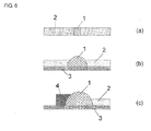
- the form in which a space for connection holds the solution is a state in which a solution 1 containing an oxide precursor is held between two end faces of optical waveguides 2 by surface tension.
- the form in which a space for structure formation is filled is a state in which the space is filled with the solution 1 containing an oxide precursor so as to connect or bond the optical waveguides 2 to each other set on a substrate 1 (or inside the substrate), or a state in which the space is filled with the solution 1 so as to connect or bond the optical waveguide 2 to a light source 4, for forming an object structure.
- the solution may be added dropwise into the space for connection or structure formation.
- the solution 1 may cover a part of the optical waveguide 2.
- the coating film formed in this manner on the lower clad portion is dried at a temperature of, for example, 25°C to 220°C before irradiation.
- a method for drying at a temperature higher than 25°C is not specifically limited, and examples of the method include a method using a hot plate or an oven in a suitable atmosphere, namely, in air, an inert gas such as nitrogen, and a vacuum.
- the drying temperature is preferably 40°C or more and more preferably 12d°C or more in order to reduce the amount of residual solvent in a coating film.
- the drying time may be 30 seconds or more and is 10 minutes or less for adequate drying.
- the drying (heat treatment) may be carried out in two or more temperature steps.
- a stepwise drying (heat treatment) further improves the uniformity of the coating film.
- the film thickness is preferably 100 nm to 400 nm in a coating film obtained by single coating. This is because a coating film having a film thickness of more than 400 nm may cause a crack in the core/clad layer, for example, by heat treatment (solvent drying) after the coating or by heat treatment during the irradiation step after that.
- the step of coating/heat treatment may be repeated until a desired film thickness is obtained.
- the completed coating film is irradiated with a radiation beam under heating.
- the radiation beam for irradiating the coating film include radiation beams (such as ultraviolet light) from a laser beam source, a mercury lamp, a metal halide lamp, a xenon lamp, and an excimer lamp.
- the irradiation amount of radiation beam can control the refractive index and the length of the manufactured core. Commonly, the irradiation amount is suitably several thousands to several tens of thousands mJ/cm 2 .
- Such radiation beam has the effect of eliminating a stabilizer.
- the stabilizer is eliminated and condensation reaction is developed immediately after that.
- the irradiated region obtains an increased refractive index to form a core.
- ultraviolet light having a short wavelength of around 254 nm is preferred because it has large energy, and thus has a large effect of accelerating the elimination of a stabilizer. Consequently, a less amount of irradiation can increase the refractive index in an area to be a core region. Furthermore, as a radiation beam having larger energy, an electron beam and the like are effectively used.
- the wavelength of a radiation beam and the heating temperature can control the shape such as width and length of a core to be manufactured.
- the coating film is irradiated with a radiation beam through a photomask under heating or is scanned with a laser beam under heating, and as a result an optical waveguide having a desired shape can be prepared in the coating films.
- a linear waveguide, a curved waveguide, a waveguide lens, a waveguide prism, and the like can be prepared.
- a 45° mirror can be prepared in the coating film. Such 45° mirror is effectively used to connect an optical waveguide in the coating film with a light source such as VCSEL, a photodetector, or a longitudinal optical waveguide.
- a mirror having another angle can be prepared by adjusting an irradiation angle in addition to the 45° mirror.
- a radiation beam is applied through an optical waveguide previously formed in the coating film or through an optical waveguide set near an end face of the coating film, it is possible to prepare in the coating film a self-organizing optical waveguide having a core that is axially aligned with that of the previously prepared optical waveguide.
- a self-organizing optical waveguide that is not axially misaligned with the light source can be prepared in the coating film.
- the light source or the optical waveguide set near an end face of the coating film may be in contact with the coating films; however, a medium such as air or a refractive index matching agent may be interposed therebetween.
- the optical waveguide used here for irradiation is not specifically limited, and a common optical waveguide can be used. However, an optical waveguide desirably has features that the optical waveguide can well transmit a radiation beam such as ultraviolet light to a coating film in the manufacturing process, and that the optical waveguide itself is not decomposed by a radiation beam.
- a radiation beam that is hard to decompose an optical waveguide used for irradiation that is, to use, for example, visible light having a wavelength of 400 nm or more, because it has small energy and therefore can suppress the decomposition of the optical waveguide.
- a coating film in an area where a self-organizing waveguide is intended to be formed is locally irradiated with visible light having a wavelength of 400 nm or more through an optical waveguide with heating, a self-organizing optical waveguide can be prepared without decomposition of the optical waveguide.
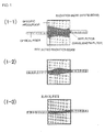
- FIG. 1 shows the principle of the reflective self-organized lightwave network (R-SOLNET).
- the R-SOLNET is a phenomenon that a self-organized lightwave network is induced by reflected light.
- a reflector that reflects a radiation beam in this case, write-beam
- write-beam a wavelength filter which reflects a write-beam and transmits a signal beam in the drawings
- the radiation beam is overlapped with the reflected radiation beam (1-1), and the refractive index in the overlapped area is increased to cause self-focusing (1-2).
- a self-organized lightwave network is drawn to the reflector, and waveguides having misaligned optical axes are automatically connected to each other (1-3) (see Tetsuzo Yoshimura and Hiroshi Kaburagi, "Self-Organization of Optical Waveguides between Misaligned Devices Induced by Write-Beam Reflection", Applied Physics Express, 1 (2008), pp. 062007 ).
- a common self-organizing optical waveguide but also the R-SOLNET can be prepared.
- a layer containing the core/clad layer can be separated from a substrate to prepare a film for use. In this case, it is attached to a semiconductor chip, a wiring board, or the like for easy integration. It is also effectively used for a three-dimensional optical circuit.
- the heating temperature during irradiation of a radiation beam is 25°C to 250°C and preferably 120°C to 250°C, as described above.
- the heat treatment accelerates the hydrolysis/condensation of a metal alkoxide to complete a core/clad layer.
- Time required for the heat treatment is usually 5 to 60 minutes and may be 10 minutes. When a low heating temperature is selected, a stable core/clad layer is readily obtained by heating for a long time.
- the core/clad layer prepared in this manner can be used as an optical waveguide without any treatment when air is regarded as an upper clad portion.
- an upper clad portion is usually formed using a resin and the like to cover the core/clad layer.
- the upper clad portion desirably has substantially the same refractive index and physical properties as those of the clad region in the core/clad layer as with the lower clad portion described above.
- an upper clad portion having the same composition as that of the clad region in the core/clad layer can be prepared. This case is preferred because the same coating solution can be used for the core/clad layer and the upper clad portion and consequently the number of materials can be reduced.
- the coating solution 1 was applied to a glass substrate by spin coating, and then the coated substrate was treated with heat on a hot plate at 200°C for removing the solvents in the coating film to form a coating film having a film thickness of 240 nm.
- the coating film was irradiated with ultraviolet light having a light intensity of 5 m W/cm 2 at a wavelength of 365 nm using a metal halide lamp (LC-8 manufactured by Hamamatsu Photonics K.K.) at 750 mJ/cm 2 while heating at 200°C.
- LC-8 metal halide lamp manufactured by Hamamatsu Photonics K.K.
- each of a coating film irradiated with ultraviolet light having a light intensity of 5 mW/cm 2 at a wavelength of 365 nm at 2250 mJ / cm 2 and a coating film without irradiation of ultraviolet light was formed on the substrate.
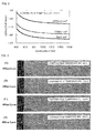
- Each refractive index of these three coating films was determined using an ellipsometer (M-2000 VI manufactured by J.A. Woollam) in a wavelength range from 400 nm to 1600 nm.
- Table 1 shows the refractive indexes at wavelengths of 650 nm, 850 nm, 1310 nm, and 1550 nm
- FIG. 2 shows the refractive index changes in a wavelength range from 400 nm to 1600 nm.
- the coating solution 1 prepared in Preparation Example 1 was applied by spin coating.
- the SiO 2 film was used as a lower clad portion here.
- the silicon wafer was moved onto a hot plate, and treated with heat at 80°C for 3 minutes and then at 200°C for 15 minutes for removing the solvents in the coating film to form a coating film.
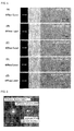
- a laser beam at a wavelength of 405 nm having various light intensities shown below was applied for various amounts of irradiation time shown below through a single mode fiber from an end face of the coating film to prepare a self-organizing optical waveguide.
- the self-organizing optical waveguide was treated with heat on a hot plate at 200°C for 15 minutes to increase a relative refractive index difference between the core and the clad.
- an upper clad portion was not prepared to leave air.
- the self-organizing optical waveguide was observed from the upper clad portion of the optical waveguide (from the air layer) under a microscope.
- a coating film was formed on a silicon wafer in a similar procedure to that in Example 1, and subsequently a part of the coating film was chipped off to prepare a defect.
- a silver paste was inserted to prepare a block of the silver paste as a reflector in the coating film.
- a laser beam at a wavelength of 405 nm having a light intensity of 0.5 mW/cm 2 was applied for an irradiation time of 50 seconds at an irradiation amount of 2.5 mJ/cm 2 through a single mode fiber from an end face of the coating film to prepare an R-SOLNET.
- an upper clad portion was not prepared to leave air.
- the R-SOLNET was observed from the upper clad portion of the optical waveguide (from the air layer) under a microscope. The result is shown in FIG. 5 .
- each refractive index difference ( ⁇ n) of the coating film irradiated with ultraviolet light at 2250 mJ/cm 2 and the coating film without irradiation of ultraviolet light (0 mJ/cm 2 ) was 10.0% or more in each wavelength.
- the optical waveguide prepared according to the present invention obtains a refractive index difference larger than that of an optical waveguide using a related art resin compound in a wide wavelength range including all of 1310 nm and 1550 nm that are so-called communication wavelengths and of 850 nm that has been studied for using as interconnect.
- Such high confinement optical waveguide having a high ⁇ n value can be used for connecting between optical waveguides having a relatively low ⁇ n value, such as optical fibers, but in specific, can provide its characteristics for connecting between wiring layers of optical wiring in a chip having a high ⁇ n value.
- the length required for connecting a self-organizing optical waveguide in the optical wiring in a chip is considered to correspond to the thickness (about 300 nm) of global wiring of common electrical wiring in a chip.
- the optical waveguide prepared according to the present invention has an enough length and is practicable.
- each tapered shape shown in FIGS. 4A to 4D is caused by a convergent radiation beam from an optical fiber due to a self-formed core and is a shape of a typical self-organizing optical waveguide.
- a self-organizing optical waveguide having a large optical confinement effect can be readily manufacture.
- Such optical waveguide is effectively used for downsizing base stations in optical fiber communication and optical communication devices such as routers and splitters in residences. It is also effectively used for the application requiring high density wiring, such as a central processing unit and memory in a computer and a printed circuit board.
Landscapes
- Physics & Mathematics (AREA)
- Engineering & Computer Science (AREA)
- Optics & Photonics (AREA)
- General Physics & Mathematics (AREA)
- Microelectronics & Electronic Packaging (AREA)
- Chemical & Material Sciences (AREA)
- Nanotechnology (AREA)
- Life Sciences & Earth Sciences (AREA)
- Biophysics (AREA)
- Crystallography & Structural Chemistry (AREA)
- Optical Integrated Circuits (AREA)
Applications Claiming Priority (2)
| Application Number | Priority Date | Filing Date | Title |
|---|---|---|---|
| JP2008223236 | 2008-09-01 | ||
| PCT/JP2009/064967 WO2010024336A1 (fr) | 2008-09-01 | 2009-08-27 | Procédé de fabrication d'un guide d'ondes optiques |
Publications (1)
| Publication Number | Publication Date |
|---|---|
| EP2333596A1 true EP2333596A1 (fr) | 2011-06-15 |
Family
ID=41721501
Family Applications (1)
| Application Number | Title | Priority Date | Filing Date |
|---|---|---|---|
| EP09809986A Withdrawn EP2333596A1 (fr) | 2008-09-01 | 2009-08-27 | Procédé de fabrication d'un guide d'ondes optiques |
Country Status (5)
| Country | Link |
|---|---|
| US (1) | US20110177259A1 (fr) |
| EP (1) | EP2333596A1 (fr) |
| JP (1) | JPWO2010024336A1 (fr) |
| TW (1) | TW201022752A (fr) |
| WO (1) | WO2010024336A1 (fr) |
Cited By (1)
| Publication number | Priority date | Publication date | Assignee | Title |
|---|---|---|---|---|
| US20220026641A1 (en) * | 2019-04-11 | 2022-01-27 | Adamant Namiki Precision Jewel Co., Ltd. | Optical connector and optical connector manufacturing method |
Families Citing this family (4)
| Publication number | Priority date | Publication date | Assignee | Title |
|---|---|---|---|---|
| JP2018185492A (ja) * | 2017-04-27 | 2018-11-22 | 株式会社豊田中央研究所 | 光部品およびその製造方法 |
| JP6534699B2 (ja) * | 2017-04-27 | 2019-06-26 | 株式会社豊田中央研究所 | 光回路およびその製造方法 |
| WO2021199377A1 (fr) * | 2020-04-01 | 2021-10-07 | 日本電信電話株式会社 | Élément de connexion optique, élément optique et procédé de fabrication d'élément optique |
| WO2026033721A1 (fr) * | 2024-08-08 | 2026-02-12 | Ntt株式会社 | Structure de connexion optique et son procédé de fabrication |
Family Cites Families (18)
| Publication number | Priority date | Publication date | Assignee | Title |
|---|---|---|---|---|
| EP1315006A1 (fr) * | 1994-06-22 | 2003-05-28 | Fujitsu Limited | Procédé de fabrication de système à guide d'onde optique, élément et coupleur optique l'utilisant, réseau optique et panneau à circuit optique |
| JPH07331173A (ja) * | 1995-02-21 | 1995-12-19 | Toray Ind Inc | 光学材料形成用塗液組成物および光学材料 |
| JPH0926514A (ja) * | 1995-07-12 | 1997-01-28 | Nippon Steel Corp | 三次元光導波路用薄膜材料およびその作製方法 |
| US6446467B1 (en) * | 1997-07-29 | 2002-09-10 | Physical Optics Corporation | Monolithic glass light shaping diffuser and method for its production |
| US6054253A (en) * | 1997-10-10 | 2000-04-25 | Mcgill University-The Royal Institute For The Advancement Of Learning | Solvent-assisted lithographic process using photosensitive sol-gel derived glass for depositing ridge waveguides on silicon |
| US6445837B1 (en) * | 1999-03-31 | 2002-09-03 | Nu-Wave Photonics, Inc. | Hybrid opto-electronic circuits and method of making |
| TW581746B (en) * | 1999-11-12 | 2004-04-01 | Nippon Sheet Glass Co Ltd | Photosensitive composition, optical waveguide element and production process therefor |
| US7016589B2 (en) * | 2000-05-19 | 2006-03-21 | Optinetrics, Inc. | Thermally-assisted photo-lithographic process using sol-gel derived glass and products made thereby |
| JP3959735B2 (ja) * | 2001-03-13 | 2007-08-15 | Jsr株式会社 | 感放射線性屈折率変化性組成物およびその利用 |
| RU2275401C2 (ru) * | 2001-03-13 | 2006-04-27 | Джей Эс Эр КОРПОРЕЙШН | Радиационно-чувстивительная композиция, изменяющая показатель преломления, и ее применение |
| JP4174987B2 (ja) * | 2001-12-17 | 2008-11-05 | Jsr株式会社 | 光導波路形成用光硬化性組成物、光導波路の形成方法、および光導波路 |
| JP2003195075A (ja) * | 2001-12-26 | 2003-07-09 | Jsr Corp | 光導波路 |
| JP2004157305A (ja) * | 2002-11-06 | 2004-06-03 | Hitachi Cable Ltd | ポリマ光導波路及びその製造方法 |
| JP2005010758A (ja) * | 2003-05-23 | 2005-01-13 | Sanyo Electric Co Ltd | 光デバイスおよびその製造方法 |
| JP4529669B2 (ja) * | 2004-12-10 | 2010-08-25 | 東洋インキ製造株式会社 | 光導波路形成用材料、光導波路の製造方法、および光導波路 |
| WO2006057298A1 (fr) * | 2004-11-26 | 2006-06-01 | Toyo Ink Mfg. Co., Ltd. | Composition polymerisable |
| WO2006138587A2 (fr) * | 2005-06-18 | 2006-12-28 | The Regents Of The University Of Colorado, A Body Corporate | Lithographie a ecriture directe en trois dimensions |
| JP2009210704A (ja) * | 2008-03-03 | 2009-09-17 | Nissan Chem Ind Ltd | 光導波路及びその製造方法 |
-
2009
- 2009-08-27 EP EP09809986A patent/EP2333596A1/fr not_active Withdrawn
- 2009-08-27 US US13/061,369 patent/US20110177259A1/en not_active Abandoned
- 2009-08-27 JP JP2010526761A patent/JPWO2010024336A1/ja active Pending
- 2009-08-27 WO PCT/JP2009/064967 patent/WO2010024336A1/fr not_active Ceased
- 2009-09-01 TW TW098129402A patent/TW201022752A/zh unknown
Non-Patent Citations (1)
| Title |
|---|
| See references of WO2010024336A1 * |
Cited By (2)
| Publication number | Priority date | Publication date | Assignee | Title |
|---|---|---|---|---|
| US20220026641A1 (en) * | 2019-04-11 | 2022-01-27 | Adamant Namiki Precision Jewel Co., Ltd. | Optical connector and optical connector manufacturing method |
| US11782216B2 (en) * | 2019-04-11 | 2023-10-10 | Orbray Co., Ltd. | Optical connector and optical connector manufacturing method |
Also Published As
| Publication number | Publication date |
|---|---|
| US20110177259A1 (en) | 2011-07-21 |
| TW201022752A (en) | 2010-06-16 |
| WO2010024336A1 (fr) | 2010-03-04 |
| JPWO2010024336A1 (ja) | 2012-01-26 |
Similar Documents
| Publication | Publication Date | Title |
|---|---|---|
| US6832036B2 (en) | Siloxane optical waveguides | |
| EP1840095B1 (fr) | Dispersions de revêtement pour fibres optiques | |
| KR100600630B1 (ko) | 저유전율 실리카계 피막 형성용 도포액 및 저유전율피막으로 도포된 기재 | |
| JP4651935B2 (ja) | 活性エネルギー線硬化型オルガノポリシロキサン樹脂組成物、光伝送部材および光伝送部材の製造方法 | |
| EP1846479B1 (fr) | Revetement en resine de siloxane | |
| EP2333596A1 (fr) | Procédé de fabrication d'un guide d'ondes optiques | |
| JP2999603B2 (ja) | スピンオングラス組成物、ハードマスクおよびハードマスク製造法 | |
| CN103443674B (zh) | 光波导用树脂组合物、以及使用该树脂组合物的干膜、光波导和光电复合电路板 | |
| JP2002026431A (ja) | レーザー装置及びこれを用いた光信号増幅装置 | |
| JP4477825B2 (ja) | 基板上に多層化した導波管素子とその製造方法 | |
| CN1773313A (zh) | 波导组合物及由其形成的波导 | |
| Du et al. | Sol-gel waveguide fabrication parameters: an experimental investigation | |
| US20030215203A1 (en) | Polysilane thin films for directly patternable waveguides | |
| US6965006B2 (en) | Metal alkoxide polymers | |
| WO2001051992A1 (fr) | Procede servant a fabriquer un article revetu par une couche portant des motifs et composition photosensible | |
| JP3273519B2 (ja) | ポリシロキサン系光導波路の製造方法 | |
| Moreira et al. | Hybrid sol-gel channel waveguide patterning using photoinitiator-free materials | |
| JP2009210704A (ja) | 光導波路及びその製造方法 | |
| JP2003014965A (ja) | レーザ直接描画導波路及びその製造方法 | |
| JP2011180464A (ja) | 光導波路の製造方法 | |
| US6319551B1 (en) | Methods and compositions for forming silica, germanosilicate and metal silicate films, patterns and multilayers | |
| Segawa et al. | Design of organic-inorganic hybrid waveguide | |
| JP2005126497A (ja) | 光導波路用感光性樹脂組成物および光導波路 | |
| JP3724391B2 (ja) | ポリマ導波路の製造方法 | |
| CN119472169A (zh) | 玻璃光刻胶、玻璃光刻胶制备方法以及飞秒激光制备方法 |
Legal Events
| Date | Code | Title | Description |
|---|---|---|---|
| PUAI | Public reference made under article 153(3) epc to a published international application that has entered the european phase |
Free format text: ORIGINAL CODE: 0009012 |
|
| 17P | Request for examination filed |
Effective date: 20110331 |
|
| AK | Designated contracting states |
Kind code of ref document: A1 Designated state(s): AT BE BG CH CY CZ DE DK EE ES FI FR GB GR HR HU IE IS IT LI LT LU LV MC MK MT NL NO PL PT RO SE SI SK SM TR |
|
| AX | Request for extension of the european patent |
Extension state: AL BA RS |
|
| DAX | Request for extension of the european patent (deleted) | ||
| STAA | Information on the status of an ep patent application or granted ep patent |
Free format text: STATUS: THE APPLICATION IS DEEMED TO BE WITHDRAWN |
|
| 18D | Application deemed to be withdrawn |
Effective date: 20130301 |