EP2333954A1 - Récupération de l'horloge dans un dispositif alimenté par batterie - Google Patents
Récupération de l'horloge dans un dispositif alimenté par batterie Download PDFInfo
- Publication number
- EP2333954A1 EP2333954A1 EP20100161688 EP10161688A EP2333954A1 EP 2333954 A1 EP2333954 A1 EP 2333954A1 EP 20100161688 EP20100161688 EP 20100161688 EP 10161688 A EP10161688 A EP 10161688A EP 2333954 A1 EP2333954 A1 EP 2333954A1
- Authority
- EP
- European Patent Office
- Prior art keywords
- counter
- time period
- oscillator
- during
- value
- Prior art date
- Legal status (The legal status is an assumption and is not a legal conclusion. Google has not performed a legal analysis and makes no representation as to the accuracy of the status listed.)
- Granted
Links
Images





Classifications
-
- H—ELECTRICITY
- H03—ELECTRONIC CIRCUITRY
- H03K—PULSE TECHNIQUE
- H03K5/00—Manipulating of pulses not covered by one of the other main groups of this subclass
-
- G—PHYSICS
- G06—COMPUTING OR CALCULATING; COUNTING
- G06F—ELECTRIC DIGITAL DATA PROCESSING
- G06F1/00—Details not covered by groups G06F3/00 - G06F13/00 and G06F21/00
- G06F1/04—Generating or distributing clock signals or signals derived directly therefrom
- G06F1/14—Time supervision arrangements, e.g. real time clock
-
- G—PHYSICS
- G06—COMPUTING OR CALCULATING; COUNTING
- G06F—ELECTRIC DIGITAL DATA PROCESSING
- G06F1/00—Details not covered by groups G06F3/00 - G06F13/00 and G06F21/00
- G06F1/26—Power supply means, e.g. regulation thereof
- G06F1/30—Means for acting in the event of power-supply failure or interruption, e.g. power-supply fluctuations
-
- H—ELECTRICITY
- H03—ELECTRONIC CIRCUITRY
- H03L—AUTOMATIC CONTROL, STARTING, SYNCHRONISATION OR STABILISATION OF GENERATORS OF ELECTRONIC OSCILLATIONS OR PULSES
- H03L7/00—Automatic control of frequency or phase; Synchronisation
- H03L7/06—Automatic control of frequency or phase; Synchronisation using a reference signal applied to a frequency- or phase-locked loop
- H03L7/08—Details of the phase-locked loop
- H03L7/081—Details of the phase-locked loop provided with an additional controlled phase shifter
- H03L7/0812—Details of the phase-locked loop provided with an additional controlled phase shifter and where no voltage or current controlled oscillator is used
Definitions
- This invention relates to clock recovery in a battery powered device, and in particular to a method for recovering a time count in the event that the battery is removed from the device.
- US-6,124,764 discloses a device having a second oscillator, which is operable with low power during sleep periods.
- the low power oscillator is calibrated against the main oscillator of the device during wake-up periods.
- a method of updating a first counter in an electronic device, a value of the first counter representing a time comprising:
- an electronic device comprising:
- the second oscillator is effectively being calibrated against the first oscillator, with the result that the duration of the recovery period can be accurately controlled, even though the second oscillator may not be well characterized.
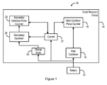
- Figure 1 shows a part of a wireless communications device 10 in accordance with an aspect of the present invention.
- the wireless communications device 10 is powered by a battery 12, and is largely conventional, and is therefore described here only so far as is necessary for an understanding of the present invention.
- Figure 1 shows the detail of a clock recovery circuit 14, which is used for counting time, including during periods when the battery 12 is removed from the device 10 for short periods, for example for replacement of the battery itself, or for replacement of a SIM card that is physically covered by the battery 12.
- the clock recovery circuit 14 includes a main oscillator 16, which may also be used to generate signals at particular frequencies for use in radio frequency communications.
- the use of the main oscillator 16 is to generate pulses at a known frequency. These pulses are supplied to a main oscillator pulse counter 18, which counts the pulses from the main oscillator 16. The number of counted pulses is used as an indication of the time of day, and this can be used by various applications running on the device 10, such as an alarm.
- pulses generated by the main oscillator 16 are counted by the main oscillator pulse counter 18 at an increased rate for the recovery period.
- the increased rate is set so that, at the end of the recovery period, the count of pulses generated by the main oscillator has recovered to the value that it would have reached if the battery had not been removed.
- FIG. 2 is a more detailed schematic diagram of the clock recovery circuit 14 and associated circuitry.
- the battery 12 is connected through a low power (LP) low dropout (LDO) regulator 28 to a pin 30, which is connected to the oscillator circuit 16 to provide power thereto.
- the oscillator circuit 16 is connected to a crystal oscillator 32, and is able to generate pulses at a frequency of 32.768 kHz.
- the oscillator 16 is connected to the main oscillator counter 18 through a switch 34. Pulses from the oscillator 16 are passed to a first input of the switch 34 through a divide-by-2 block 36 and are passed undivided to a second input of the switch 34.
- the regulator 28 is also connected to the charge store 20, which includes a small backup capacitor 37 for storing the charge and a resistor 38.
- the charge store 20 is also connected to a pin 40, which is connected to the secondary low-power oscillator circuit 24 to provide power thereto.
- the secondary oscillator 24 can be of relatively low precision, meaning that its frequency might not be known to a high degree of accuracy, because of initial tolerances and temperature drift, but it might for example be in the range of 26-56 kHz.
- the secondary oscillator 24 may be a very low power simple oscillator, such as an RC circuit, which can be implemented completely internal to an ASIC that contains the clock recovery circuit 14. As described below, the secondary oscillator 24 does not require any factory calibration, or any other calibration prior to use.
- the secondary oscillator 24 is connected to the secondary counter 26.
- the secondary oscillator 24 is connected to a stability counter 42, which also receives an enable input from a threshold circuit 44, which provides a signal when it detects that the voltage from the battery 12 has fallen below the threshold value, namely when the battery 12 has been removed.
- the outputs from the threshold circuit 44 and the stability counter 42 are also passed to an OR gate 46.
- the output from the OR gate 46 is passed through an inverter 48 to an enable input of the first counter 18.
- the output from the OR gate 46 is also passed to an up/down control input of the second counter 26.
- the second counter 26 provides an output on its output terminal 50 when its count value is greater than zero.
- the output from the OR gate 46, and the signal on the output terminal 50 of the second counter 26 are combined in a further OR gate 52, with the result being passed to an enable input of the second counter 26.
- the circuit shown in Figure 2 also allows an alarm value, that is, a time value at which an alarm is requested by the user, to be set in the alarm register 54, and includes a comparator 56, for determining when the count value in the main counter 18 reaches the set alarm value, so that an alarm can be generated.
- an alarm value that is, a time value at which an alarm is requested by the user
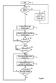
- FIG 3 shows the process performed by the circuit of Figure 2 in this embodiment.
- the process starts at step 70, when the device 10 is in operation.
- step 72 it is determined whether the battery 12 is present. If the battery is present, the voltage V BATT is greater than the threshold voltage V TH , as shown by line 90 in Figure 4 .
- pulses are generated by the main oscillator 16, and the main counter 18 is enabled, so that the pulses are counted, as shown at step 74 in Figure 3 , and the main count value is continuously increasing, as shown by line 96 in Figure 4 .
- the secondary counter 26 has not been enabled, and so the secondary count value is not greater than zero, and so the switch 34 is controlled so that the pulses generated by the main oscillator 16 are passed through the divide-by-2 block 36, with the result that the pulses are counted at a first rate, which is a fraction, in this case one half, of the rate at which they are generated.
- the voltage V BATT soon falls below the threshold voltage V TH , at the time T 1 shown in Figure 4 . At this time, it is determined that the battery 12 is not present. At this point, it is no longer possible to rely on the main oscillator 16 to provide pulses at the intended frequency, even if it is still able to generate some pulses.
- the threshold block 44 When the voltage V BATT falls below the threshold voltage V TH , the threshold block 44 outputs a positive signal V A , as shown by the line 92 in Figure 4 .
- the OR gate 46 provides a positive output, which is inverted by the inverter 48, so that the positive signal is removed from the enable input of the main counter 18, thereby disabling the count of the main oscillator pulses, as shown at step 76 in Figure 3 .
- the effect of this is that the main count value 96 is frozen, and remains constant after T 1 , as shown in Figure 4 .
- the positive output of the OR gate 46 causes the OR gate 52 to generate a positive input for the enable input of the secondary counter 26, and is also passed to the up/down input of the secondary counter.
- the result is that pulses generated by the secondary oscillator 24, which is receiving its power from the backup charge store 20, are counted up in the secondary oscillator 24, as shown at step 78 in Figure 3 .
- the secondary count value 98 thus increases after T 1 .
- the counter 42 continues to count pulses from the secondary oscillator 24 for a stabilization time period, until the main oscillator 16 has restarted stable operation. It is only when the stabilization time period expires, as determined at step 82 in Figure 3 , at the time T 2 shown in Figure 4 , that the voltage V B falls to zero, as shown by line 94 in Figure 4 .
- the stabilization period set by the counter 42 therefore effectively forms part of the battery removal period, in this embodiment.
- the secondary count value is positive, and so the switch 34 is controlled so that the pulses generated by the main oscillator 16 are not passed through the divide-by-2 block 36, with the result that the pulses are passed through at a second rate, which is equal to the rate at which they are generated.
- the voltages V A and V B are both zero, and so there is no positive output from the OR gate 46.
- the inverter 48 therefore causes a signal to be passed to the enable input of the main counter 18, with the result that the main oscillator pulses are counted at the second rate, as shown at step 84 of Figure 3 .
- the effect of this is that the main count value 96 increases after time T 2 at a rate which is double the rate at which it increased before T 1 .
- the zero output from the OR gate 46 is passed to the up/down input of the secondary counter, and so the pulses received at the secondary counter 26 are now used to decrement the count value, as shown at step 86 of Figure 3 .
- the secondary oscillator 24 has a relatively wide tolerance, and its frequency may drift greatly with temperature, its frequency can be assumed to be constant during the relatively short period while the battery 12 is removed.
- the effect of this process is that, although the maximum value of the secondary count that is reached at time T 2 cannot be relied upon to have any particular meaning, the lengths of the battery removal period (including the stabilization period in this embodiment), T 1 -T 2 , and the recovery period T 2 -T 3 , can be assumed to be equal.
- the main count value is not increased during the battery removal period, but increases at twice the normal rate during the recovery period, the main count value will return by time T 3 to the value that it would have reached if it had been allowed to continue increasing at the normal rate for the whole period.
- the count value can therefore be used as a measure of the time of day. For example, it can be compared with the set alarm time, and the alarm can be generated when the count value is found by the comparator 56 to be equal to the value stored in the register 54. Although any alarm that was scheduled to occur during the battery removal period or during the recovery period will now occur later in the recovery period, the difference will be small provided that the battery removal period has a short duration. Any alarm that was scheduled to occur during the recovery period will occur at the intended time.
- Y is advantageously an integer power of 2, so that the block 36 can be replaced by any divide-by-Y block, which can then be implemented relatively simply by means of a binary counter.
- circuit shown in Figure 5 is generally similar to that shown in Figure 2 , and components having the same functions are indicated by the same reference numerals, and will not be described further herein.
- pulses from the main oscillator 16 are passed to the first input of the switch 34 through a divide-by-4 block 110, and are passed undivided to the second input of the switch 34.
- pulses from the secondary oscillator 24 are passed to a first input of a switch 112 through a divide-by-3 block 114 and are passed undivided to a second input of the switch 112.
- the output of the switch 112 is connected to the input of the secondary counter 26, and the switch 112 is controlled by the output of the OR gate 46.
- Figure 6 illustrates the operation of the circuit of Figure 5 .
- the switch 112 is controlled so that the pulses from the secondary oscillator 24 that have passed through the divide-by-3 block 114 are passed to the input of the secondary counter 26.
- the result is that the secondary count value increases at one third of the rate at which it increased in Figure 4 (the vertical scales of Figures 4 and 6 are not the same, so that this difference is not apparent).
- the switch 112 is controlled so that the pulses from the secondary oscillator 24 that have not passed through the divide-by-3 block 114 are passed to the input of the secondary counter 26.
- the secondary count value decrements at three times the rate at which it increased during the battery removal period, and hence that the duration of the recovery period T 2 -T 4 is one third of the duration of the battery removal period T 1 -T 2 .
- the fact that the pulses from the main oscillator 16 that are counted have been passed to the main counter 18 through the divide-by-4 block 110 before the time T 1 , and have not been passed through the divide-by-4 block 110 during the recovery period means that the main count value increases during the recovery period at a second rate that is four times the normal rate.
- Figure 7 is a circuit diagram of a further embodiment, in which this is possible.
- the circuit shown in Figure 7 is generally similar to that shown in Figure 2 , and components having the same functions are indicated by the same reference numerals, and will not be described further herein.
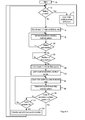
- Figure 8 is a flow chart, illustrating the method of operation of the circuit of Figure 7 .
- the method of Figure 8 is generally similar to that shown in Figure 3 , and corresponding steps are indicated by the same reference numerals, and will not be described further herein.
- a main count latch 120 is connected to the main counter 18, and a secondary count latch 122 is connected to the secondary counter 26.
- the main count value is latched in step 130 and the secondary count value is latched in step 132, at the time T 2 . Then, while the secondary count value is decrementing during the recovery period, it is determined in step 134 whether the device has been powered on. If so, then, in step 136, at time T 5 , a main count correction value C 1 is calculated, the main count correction value C 1 being the value that needs to be added to the main count value in order to bring it up to the value that it would have reached if it had been incrementing at the first rate throughout the battery removal period and the recovery period to date. The process then returns to the start.
- This correction value can be calculated with sufficient accuracy, provided that the recovery period has been running for long enough that the division by the term (SC L - SC F ) does not introduce any significant error.
- SC L - SC F the division by the term
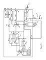
- pulses from the main oscillator 16 are passed to the first input of the switch 34 through a divide-by-4 block 150, and are passed undivided to the second input of the switch 34.
- pulses from the secondary oscillator 24 are passed to a first input of a switch 152 through a divide-by-3 block 154 and are passed undivided to a second input of the switch 152.
- the output of the switch 152 is connected to the input of the secondary counter 26, and the switch 152 is controlled by the output of the OR gate 46.
- Figure 11 illustrates the operation of the circuit of Figure 10 .
- the switch 152 is controlled so that the pulses from the secondary oscillator 24 that have passed through the divide-by-3 block 154 are passed to the input of the secondary counter 26.
- the result is that the secondary count value increases at one third of the rate at which it increased in Figure 9 (the vertical scales of Figures 9 and 11 are not the same, so that this difference is not apparent).
- the switch 152 is controlled so that the pulses from the secondary oscillator 24 that have not passed through the divide-by-3 block 154 are passed to the input of the secondary counter 26.
- the result is that the secondary count value decrements at three times the rate at which it increased during the battery removal period, and hence that the maximum duration of the recovery period is one third of the duration of the battery removal period T 1 -T 2 .
Landscapes
- Engineering & Computer Science (AREA)
- Theoretical Computer Science (AREA)
- Physics & Mathematics (AREA)
- General Engineering & Computer Science (AREA)
- General Physics & Mathematics (AREA)
- Nonlinear Science (AREA)
- Charge And Discharge Circuits For Batteries Or The Like (AREA)
Priority Applications (3)
| Application Number | Priority Date | Filing Date | Title |
|---|---|---|---|
| PCT/GB2010/051962 WO2011064583A1 (fr) | 2009-11-25 | 2010-11-24 | Rétablissement de l'horloge dans un dispositif alimenté par pile |
| KR1020127013417A KR101709821B1 (ko) | 2009-11-25 | 2010-11-24 | 전자 디바이스 내의 제 1 카운터를 업데이트하는 방법 및 전자 디바이스 |
| US13/508,572 US8630386B2 (en) | 2009-11-25 | 2010-11-24 | Clock recovery in a battery powered device |
Applications Claiming Priority (1)
| Application Number | Priority Date | Filing Date | Title |
|---|---|---|---|
| US26444509P | 2009-11-25 | 2009-11-25 |
Publications (2)
| Publication Number | Publication Date |
|---|---|
| EP2333954A1 true EP2333954A1 (fr) | 2011-06-15 |
| EP2333954B1 EP2333954B1 (fr) | 2015-07-22 |
Family
ID=43607864
Family Applications (1)
| Application Number | Title | Priority Date | Filing Date |
|---|---|---|---|
| EP10161688.6A Active EP2333954B1 (fr) | 2009-11-25 | 2010-04-30 | Récupération de l'horloge dans un dispositif alimenté par batterie |
Country Status (4)
| Country | Link |
|---|---|
| US (1) | US8630386B2 (fr) |
| EP (1) | EP2333954B1 (fr) |
| KR (1) | KR101709821B1 (fr) |
| WO (1) | WO2011064583A1 (fr) |
Families Citing this family (2)
| Publication number | Priority date | Publication date | Assignee | Title |
|---|---|---|---|---|
| US8749313B2 (en) * | 2011-06-03 | 2014-06-10 | St-Ericsson Sa | Correction of low accuracy clock |
| US9250695B2 (en) * | 2013-03-15 | 2016-02-02 | Google Technology Holdings LLC | Method and apparatus for displaying a predetermined image on a display panel of an electronic device when the electronic device is operating in a reduced power mode of operation |
Citations (5)
| Publication number | Priority date | Publication date | Assignee | Title |
|---|---|---|---|---|
| WO1998020620A1 (fr) * | 1996-11-07 | 1998-05-14 | Telefonaktiebolaget Lm Ericsson (Publ) | Procede et appareil de reduction du courant en mode de veille dans un equipement de telecommunications |
| US6124764A (en) | 1999-01-22 | 2000-09-26 | Telefonaktiebolaget Lm Ericsson | Stable low-power oscillator |
| US20020065117A1 (en) * | 2000-11-29 | 2002-05-30 | Nec Corporation | Mobile phone capable of stopping main clock signal |
| EP1248373A1 (fr) * | 2000-04-04 | 2002-10-09 | Texas Instruments Incorporated | Appareil et procédé de génération d'une horloge à partir d'une horloge de fréquence arbitraire |
| US6603365B1 (en) | 2002-03-28 | 2003-08-05 | Denso Corporation | Real-time clock backup |
Family Cites Families (5)
| Publication number | Priority date | Publication date | Assignee | Title |
|---|---|---|---|---|
| US6029061A (en) * | 1997-03-11 | 2000-02-22 | Lucent Technologies Inc. | Power saving scheme for a digital wireless communications terminal |
| US6044282A (en) * | 1997-08-15 | 2000-03-28 | Sharp Laboratories Of America, Inc. | Dual clock power conservation system and method for timing synchronous communications |
| US6725067B1 (en) * | 2000-03-24 | 2004-04-20 | International Business Machines Corporation | Method and system for restarting a reference clock of a mobile station after a sleep period with a zero mean time error |
| TWI228885B (en) * | 2003-01-23 | 2005-03-01 | Mediatek Inc | Method for controlling a mobile communication device to enter a power-saving mode and to recover timing after the mobile communication device leaves the power-saving mode |
| US7340634B2 (en) * | 2004-08-27 | 2008-03-04 | Lsi Logic Corporation | Real time clock architecture and/or method for a system on a chip (SOC) application |
-
2010
- 2010-04-30 EP EP10161688.6A patent/EP2333954B1/fr active Active
- 2010-11-24 WO PCT/GB2010/051962 patent/WO2011064583A1/fr not_active Ceased
- 2010-11-24 KR KR1020127013417A patent/KR101709821B1/ko active Active
- 2010-11-24 US US13/508,572 patent/US8630386B2/en active Active
Patent Citations (5)
| Publication number | Priority date | Publication date | Assignee | Title |
|---|---|---|---|---|
| WO1998020620A1 (fr) * | 1996-11-07 | 1998-05-14 | Telefonaktiebolaget Lm Ericsson (Publ) | Procede et appareil de reduction du courant en mode de veille dans un equipement de telecommunications |
| US6124764A (en) | 1999-01-22 | 2000-09-26 | Telefonaktiebolaget Lm Ericsson | Stable low-power oscillator |
| EP1248373A1 (fr) * | 2000-04-04 | 2002-10-09 | Texas Instruments Incorporated | Appareil et procédé de génération d'une horloge à partir d'une horloge de fréquence arbitraire |
| US20020065117A1 (en) * | 2000-11-29 | 2002-05-30 | Nec Corporation | Mobile phone capable of stopping main clock signal |
| US6603365B1 (en) | 2002-03-28 | 2003-08-05 | Denso Corporation | Real-time clock backup |
Also Published As
| Publication number | Publication date |
|---|---|
| US8630386B2 (en) | 2014-01-14 |
| KR20120112413A (ko) | 2012-10-11 |
| EP2333954B1 (fr) | 2015-07-22 |
| KR101709821B1 (ko) | 2017-02-23 |
| WO2011064583A1 (fr) | 2011-06-03 |
| US20120230461A1 (en) | 2012-09-13 |
Similar Documents
| Publication | Publication Date | Title |
|---|---|---|
| CN109067394B (zh) | 片上时钟校准装置及校准方法 | |
| US10172092B1 (en) | Systems and methods for providing a sleep clock on a wireless communications device | |
| US8749313B2 (en) | Correction of low accuracy clock | |
| KR100687230B1 (ko) | 알티씨 장치 및 알티씨 장치의 현재시각 보정 방법 | |
| CN113346881B (zh) | 数字时钟校准方法、无线遥控器及存储介质 | |
| CN102981551B (zh) | 一种实时时钟温度补偿系统及方法 | |
| EP1585223B1 (fr) | Méthode et circuit pour déterminer un facteur de calibration pour une horloge lente | |
| EP2854294A1 (fr) | Générateur de signal de synchronisation à compensation de température | |
| EP2333954B1 (fr) | Récupération de l'horloge dans un dispositif alimenté par batterie | |
| US6326825B1 (en) | Accurate time delay system and method utilizing an inaccurate oscillator | |
| US10739731B2 (en) | Electronic timepiece, display control method and storage medium | |
| US8917147B2 (en) | Method and system to improve power utilization using a calibrated crystal warm-up detection | |
| US6618456B1 (en) | Asynchronous timing oscillator re-synchronizer and method | |
| US8466751B2 (en) | High-precision and low-consumption quartz oscillator | |
| JP4952406B2 (ja) | 時刻補正方法、マイコン内部時計、電子制御ユニット | |
| CN111209712B (zh) | 一种获取晶体振荡器工作电压的系统、方法、芯片 | |
| CN110109342B (zh) | 一种晶振频率守时的方法及守时设备 | |
| US12483191B2 (en) | Method and apparatus for oscillator frequency calibration | |
| JP4976037B2 (ja) | 電波修正時計 | |
| JP5508560B2 (ja) | 電子時計 | |
| JP5205086B2 (ja) | 電子時計 | |
| JPH10332849A (ja) | 電子時計 | |
| CN120103925A (zh) | 一种高精度计时器及其计时方法 | |
| JPH07219672A (ja) | 高精度時計回路 | |
| JP2024009609A (ja) | 車載装置、プログラム及び情報処理方法 |
Legal Events
| Date | Code | Title | Description |
|---|---|---|---|
| PUAI | Public reference made under article 153(3) epc to a published international application that has entered the european phase |
Free format text: ORIGINAL CODE: 0009012 |
|
| AK | Designated contracting states |
Kind code of ref document: A1 Designated state(s): AT BE BG CH CY CZ DE DK EE ES FI FR GB GR HR HU IE IS IT LI LT LU LV MC MK MT NL NO PL PT RO SE SI SK SM TR |
|
| AX | Request for extension of the european patent |
Extension state: AL BA ME RS |
|
| 17P | Request for examination filed |
Effective date: 20111214 |
|
| GRAP | Despatch of communication of intention to grant a patent |
Free format text: ORIGINAL CODE: EPIDOSNIGR1 |
|
| INTG | Intention to grant announced |
Effective date: 20150409 |
|
| GRAS | Grant fee paid |
Free format text: ORIGINAL CODE: EPIDOSNIGR3 |
|
| GRAA | (expected) grant |
Free format text: ORIGINAL CODE: 0009210 |
|
| AK | Designated contracting states |
Kind code of ref document: B1 Designated state(s): AT BE BG CH CY CZ DE DK EE ES FI FR GB GR HR HU IE IS IT LI LT LU LV MC MK MT NL NO PL PT RO SE SI SK SM TR |
|
| REG | Reference to a national code |
Ref country code: GB Ref legal event code: FG4D |
|
| REG | Reference to a national code |
Ref country code: CH Ref legal event code: EP |
|
| REG | Reference to a national code |
Ref country code: IE Ref legal event code: FG4D |
|
| REG | Reference to a national code |
Ref country code: AT Ref legal event code: REF Ref document number: 738391 Country of ref document: AT Kind code of ref document: T Effective date: 20150815 |
|
| REG | Reference to a national code |
Ref country code: DE Ref legal event code: R096 Ref document number: 602010026009 Country of ref document: DE |
|
| REG | Reference to a national code |
Ref country code: AT Ref legal event code: MK05 Ref document number: 738391 Country of ref document: AT Kind code of ref document: T Effective date: 20150722 |
|
| REG | Reference to a national code |
Ref country code: LT Ref legal event code: MG4D |
|
| REG | Reference to a national code |
Ref country code: NL Ref legal event code: MP Effective date: 20150722 |
|
| PG25 | Lapsed in a contracting state [announced via postgrant information from national office to epo] |
Ref country code: NO Free format text: LAPSE BECAUSE OF FAILURE TO SUBMIT A TRANSLATION OF THE DESCRIPTION OR TO PAY THE FEE WITHIN THE PRESCRIBED TIME-LIMIT Effective date: 20151022 Ref country code: LT Free format text: LAPSE BECAUSE OF FAILURE TO SUBMIT A TRANSLATION OF THE DESCRIPTION OR TO PAY THE FEE WITHIN THE PRESCRIBED TIME-LIMIT Effective date: 20150722 Ref country code: GR Free format text: LAPSE BECAUSE OF FAILURE TO SUBMIT A TRANSLATION OF THE DESCRIPTION OR TO PAY THE FEE WITHIN THE PRESCRIBED TIME-LIMIT Effective date: 20151023 Ref country code: FI Free format text: LAPSE BECAUSE OF FAILURE TO SUBMIT A TRANSLATION OF THE DESCRIPTION OR TO PAY THE FEE WITHIN THE PRESCRIBED TIME-LIMIT Effective date: 20150722 Ref country code: LV Free format text: LAPSE BECAUSE OF FAILURE TO SUBMIT A TRANSLATION OF THE DESCRIPTION OR TO PAY THE FEE WITHIN THE PRESCRIBED TIME-LIMIT Effective date: 20150722 |
|
| PG25 | Lapsed in a contracting state [announced via postgrant information from national office to epo] |
Ref country code: AT Free format text: LAPSE BECAUSE OF FAILURE TO SUBMIT A TRANSLATION OF THE DESCRIPTION OR TO PAY THE FEE WITHIN THE PRESCRIBED TIME-LIMIT Effective date: 20150722 Ref country code: ES Free format text: LAPSE BECAUSE OF FAILURE TO SUBMIT A TRANSLATION OF THE DESCRIPTION OR TO PAY THE FEE WITHIN THE PRESCRIBED TIME-LIMIT Effective date: 20150722 Ref country code: PT Free format text: LAPSE BECAUSE OF FAILURE TO SUBMIT A TRANSLATION OF THE DESCRIPTION OR TO PAY THE FEE WITHIN THE PRESCRIBED TIME-LIMIT Effective date: 20151123 Ref country code: SE Free format text: LAPSE BECAUSE OF FAILURE TO SUBMIT A TRANSLATION OF THE DESCRIPTION OR TO PAY THE FEE WITHIN THE PRESCRIBED TIME-LIMIT Effective date: 20150722 Ref country code: IS Free format text: LAPSE BECAUSE OF FAILURE TO SUBMIT A TRANSLATION OF THE DESCRIPTION OR TO PAY THE FEE WITHIN THE PRESCRIBED TIME-LIMIT Effective date: 20151122 Ref country code: HR Free format text: LAPSE BECAUSE OF FAILURE TO SUBMIT A TRANSLATION OF THE DESCRIPTION OR TO PAY THE FEE WITHIN THE PRESCRIBED TIME-LIMIT Effective date: 20150722 Ref country code: PL Free format text: LAPSE BECAUSE OF FAILURE TO SUBMIT A TRANSLATION OF THE DESCRIPTION OR TO PAY THE FEE WITHIN THE PRESCRIBED TIME-LIMIT Effective date: 20150722 |
|
| REG | Reference to a national code |
Ref country code: FR Ref legal event code: PLFP Year of fee payment: 7 |
|
| REG | Reference to a national code |
Ref country code: DE Ref legal event code: R097 Ref document number: 602010026009 Country of ref document: DE |
|
| PG25 | Lapsed in a contracting state [announced via postgrant information from national office to epo] |
Ref country code: DK Free format text: LAPSE BECAUSE OF FAILURE TO SUBMIT A TRANSLATION OF THE DESCRIPTION OR TO PAY THE FEE WITHIN THE PRESCRIBED TIME-LIMIT Effective date: 20150722 Ref country code: IT Free format text: LAPSE BECAUSE OF FAILURE TO SUBMIT A TRANSLATION OF THE DESCRIPTION OR TO PAY THE FEE WITHIN THE PRESCRIBED TIME-LIMIT Effective date: 20150722 Ref country code: CZ Free format text: LAPSE BECAUSE OF FAILURE TO SUBMIT A TRANSLATION OF THE DESCRIPTION OR TO PAY THE FEE WITHIN THE PRESCRIBED TIME-LIMIT Effective date: 20150722 Ref country code: EE Free format text: LAPSE BECAUSE OF FAILURE TO SUBMIT A TRANSLATION OF THE DESCRIPTION OR TO PAY THE FEE WITHIN THE PRESCRIBED TIME-LIMIT Effective date: 20150722 Ref country code: SK Free format text: LAPSE BECAUSE OF FAILURE TO SUBMIT A TRANSLATION OF THE DESCRIPTION OR TO PAY THE FEE WITHIN THE PRESCRIBED TIME-LIMIT Effective date: 20150722 |
|
| PLBE | No opposition filed within time limit |
Free format text: ORIGINAL CODE: 0009261 |
|
| STAA | Information on the status of an ep patent application or granted ep patent |
Free format text: STATUS: NO OPPOSITION FILED WITHIN TIME LIMIT |
|
| PG25 | Lapsed in a contracting state [announced via postgrant information from national office to epo] |
Ref country code: RO Free format text: LAPSE BECAUSE OF FAILURE TO SUBMIT A TRANSLATION OF THE DESCRIPTION OR TO PAY THE FEE WITHIN THE PRESCRIBED TIME-LIMIT Effective date: 20150722 |
|
| 26N | No opposition filed |
Effective date: 20160425 |
|
| PG25 | Lapsed in a contracting state [announced via postgrant information from national office to epo] |
Ref country code: SI Free format text: LAPSE BECAUSE OF FAILURE TO SUBMIT A TRANSLATION OF THE DESCRIPTION OR TO PAY THE FEE WITHIN THE PRESCRIBED TIME-LIMIT Effective date: 20150722 Ref country code: BE Free format text: LAPSE BECAUSE OF NON-PAYMENT OF DUE FEES Effective date: 20160430 |
|
| REG | Reference to a national code |
Ref country code: CH Ref legal event code: PL |
|
| PG25 | Lapsed in a contracting state [announced via postgrant information from national office to epo] |
Ref country code: BE Free format text: LAPSE BECAUSE OF FAILURE TO SUBMIT A TRANSLATION OF THE DESCRIPTION OR TO PAY THE FEE WITHIN THE PRESCRIBED TIME-LIMIT Effective date: 20150722 Ref country code: LU Free format text: LAPSE BECAUSE OF FAILURE TO SUBMIT A TRANSLATION OF THE DESCRIPTION OR TO PAY THE FEE WITHIN THE PRESCRIBED TIME-LIMIT Effective date: 20160430 |
|
| REG | Reference to a national code |
Ref country code: DE Ref legal event code: R082 Ref document number: 602010026009 Country of ref document: DE Representative=s name: GRUENECKER PATENT- UND RECHTSANWAELTE PARTG MB, DE Ref country code: DE Ref legal event code: R081 Ref document number: 602010026009 Country of ref document: DE Owner name: OCT CIRCUIT TECHNOLOGIES INTERNATIONAL LTD., IE Free format text: FORMER OWNER: ST-ERICSSON SA, PLAN-LES-OUATES, CH |
|
| REG | Reference to a national code |
Ref country code: IE Ref legal event code: MM4A |
|
| PG25 | Lapsed in a contracting state [announced via postgrant information from national office to epo] |
Ref country code: CH Free format text: LAPSE BECAUSE OF NON-PAYMENT OF DUE FEES Effective date: 20160430 Ref country code: LI Free format text: LAPSE BECAUSE OF NON-PAYMENT OF DUE FEES Effective date: 20160430 |
|
| REG | Reference to a national code |
Ref country code: FR Ref legal event code: PLFP Year of fee payment: 8 |
|
| PG25 | Lapsed in a contracting state [announced via postgrant information from national office to epo] |
Ref country code: IE Free format text: LAPSE BECAUSE OF NON-PAYMENT OF DUE FEES Effective date: 20160430 |
|
| PG25 | Lapsed in a contracting state [announced via postgrant information from national office to epo] |
Ref country code: NL Free format text: LAPSE BECAUSE OF FAILURE TO SUBMIT A TRANSLATION OF THE DESCRIPTION OR TO PAY THE FEE WITHIN THE PRESCRIBED TIME-LIMIT Effective date: 20150722 |
|
| REG | Reference to a national code |
Ref country code: FR Ref legal event code: TP Owner name: OCT CIRCUIT TECHNOLOGIES INTERNATIONAL LIMITED, IE Effective date: 20180116 |
|
| PG25 | Lapsed in a contracting state [announced via postgrant information from national office to epo] |
Ref country code: CY Free format text: LAPSE BECAUSE OF FAILURE TO SUBMIT A TRANSLATION OF THE DESCRIPTION OR TO PAY THE FEE WITHIN THE PRESCRIBED TIME-LIMIT Effective date: 20150722 Ref country code: SM Free format text: LAPSE BECAUSE OF FAILURE TO SUBMIT A TRANSLATION OF THE DESCRIPTION OR TO PAY THE FEE WITHIN THE PRESCRIBED TIME-LIMIT Effective date: 20150722 Ref country code: HU Free format text: LAPSE BECAUSE OF FAILURE TO SUBMIT A TRANSLATION OF THE DESCRIPTION OR TO PAY THE FEE WITHIN THE PRESCRIBED TIME-LIMIT; INVALID AB INITIO Effective date: 20100430 |
|
| PG25 | Lapsed in a contracting state [announced via postgrant information from national office to epo] |
Ref country code: MK Free format text: LAPSE BECAUSE OF FAILURE TO SUBMIT A TRANSLATION OF THE DESCRIPTION OR TO PAY THE FEE WITHIN THE PRESCRIBED TIME-LIMIT Effective date: 20150722 Ref country code: TR Free format text: LAPSE BECAUSE OF FAILURE TO SUBMIT A TRANSLATION OF THE DESCRIPTION OR TO PAY THE FEE WITHIN THE PRESCRIBED TIME-LIMIT Effective date: 20150722 Ref country code: MT Free format text: LAPSE BECAUSE OF NON-PAYMENT OF DUE FEES Effective date: 20160430 Ref country code: MC Free format text: LAPSE BECAUSE OF FAILURE TO SUBMIT A TRANSLATION OF THE DESCRIPTION OR TO PAY THE FEE WITHIN THE PRESCRIBED TIME-LIMIT Effective date: 20150722 |
|
| PG25 | Lapsed in a contracting state [announced via postgrant information from national office to epo] |
Ref country code: BG Free format text: LAPSE BECAUSE OF FAILURE TO SUBMIT A TRANSLATION OF THE DESCRIPTION OR TO PAY THE FEE WITHIN THE PRESCRIBED TIME-LIMIT Effective date: 20150722 |
|
| REG | Reference to a national code |
Ref country code: FR Ref legal event code: PLFP Year of fee payment: 9 |
|
| REG | Reference to a national code |
Ref country code: GB Ref legal event code: 732E Free format text: REGISTERED BETWEEN 20210722 AND 20210728 |
|
| REG | Reference to a national code |
Ref country code: GB Ref legal event code: 732E Free format text: REGISTERED BETWEEN 20210805 AND 20210811 |
|
| PGFP | Annual fee paid to national office [announced via postgrant information from national office to epo] |
Ref country code: DE Payment date: 20250429 Year of fee payment: 16 |
|
| PGFP | Annual fee paid to national office [announced via postgrant information from national office to epo] |
Ref country code: GB Payment date: 20250428 Year of fee payment: 16 |
|
| PGFP | Annual fee paid to national office [announced via postgrant information from national office to epo] |
Ref country code: FR Payment date: 20250425 Year of fee payment: 16 |