EP2341642B1 - Procédé de transmission de données dans un canal optique - Google Patents
Procédé de transmission de données dans un canal optique Download PDFInfo
- Publication number
- EP2341642B1 EP2341642B1 EP20100305008 EP10305008A EP2341642B1 EP 2341642 B1 EP2341642 B1 EP 2341642B1 EP 20100305008 EP20100305008 EP 20100305008 EP 10305008 A EP10305008 A EP 10305008A EP 2341642 B1 EP2341642 B1 EP 2341642B1
- Authority
- EP
- European Patent Office
- Prior art keywords
- digital
- carrier wave
- binary
- optical carrier
- accordance
- Prior art date
- Legal status (The legal status is an assumption and is not a legal conclusion. Google has not performed a legal analysis and makes no representation as to the accuracy of the status listed.)
- Not-in-force
Links
- 230000003287 optical effect Effects 0.000 title claims description 122
- 238000000034 method Methods 0.000 title claims description 29
- 230000007704 transition Effects 0.000 claims description 41
- 230000000875 corresponding effect Effects 0.000 claims description 12
- 230000002596 correlated effect Effects 0.000 claims description 11
- 238000012546 transfer Methods 0.000 claims description 2
- 238000010586 diagram Methods 0.000 description 7
- 230000010287 polarization Effects 0.000 description 7
- 230000001427 coherent effect Effects 0.000 description 6
- 230000009022 nonlinear effect Effects 0.000 description 6
- 230000005540 biological transmission Effects 0.000 description 5
- 238000004891 communication Methods 0.000 description 5
- 230000009021 linear effect Effects 0.000 description 4
- 238000007476 Maximum Likelihood Methods 0.000 description 2
- 230000006735 deficit Effects 0.000 description 2
- 230000001419 dependent effect Effects 0.000 description 2
- 238000001514 detection method Methods 0.000 description 2
- 239000013307 optical fiber Substances 0.000 description 2
- 238000012545 processing Methods 0.000 description 2
- 230000005374 Kerr effect Effects 0.000 description 1
- 238000006243 chemical reaction Methods 0.000 description 1
- 230000021615 conjugation Effects 0.000 description 1
- 238000010276 construction Methods 0.000 description 1
- 238000012937 correction Methods 0.000 description 1
- 238000013500 data storage Methods 0.000 description 1
- 230000003111 delayed effect Effects 0.000 description 1
- 230000000694 effects Effects 0.000 description 1
- 238000005516 engineering process Methods 0.000 description 1
- 238000013507 mapping Methods 0.000 description 1
- 230000015654 memory Effects 0.000 description 1
- 238000012986 modification Methods 0.000 description 1
- 230000004048 modification Effects 0.000 description 1
- 230000010363 phase shift Effects 0.000 description 1
- 230000001902 propagating effect Effects 0.000 description 1
- 230000035945 sensitivity Effects 0.000 description 1
Images


Classifications
-
- H—ELECTRICITY
- H04—ELECTRIC COMMUNICATION TECHNIQUE
- H04B—TRANSMISSION
- H04B10/00—Transmission systems employing electromagnetic waves other than radio-waves, e.g. infrared, visible or ultraviolet light, or employing corpuscular radiation, e.g. quantum communication
- H04B10/50—Transmitters
- H04B10/501—Structural aspects
- H04B10/503—Laser transmitters
- H04B10/505—Laser transmitters using external modulation
-
- H—ELECTRICITY
- H04—ELECTRIC COMMUNICATION TECHNIQUE
- H04B—TRANSMISSION
- H04B10/00—Transmission systems employing electromagnetic waves other than radio-waves, e.g. infrared, visible or ultraviolet light, or employing corpuscular radiation, e.g. quantum communication
- H04B10/50—Transmitters
- H04B10/516—Details of coding or modulation
- H04B10/548—Phase or frequency modulation
- H04B10/556—Digital modulation, e.g. differential phase shift keying [DPSK] or frequency shift keying [FSK]
- H04B10/5561—Digital phase modulation
-
- H—ELECTRICITY
- H04—ELECTRIC COMMUNICATION TECHNIQUE
- H04L—TRANSMISSION OF DIGITAL INFORMATION, e.g. TELEGRAPHIC COMMUNICATION
- H04L27/00—Modulated-carrier systems
- H04L27/18—Phase-modulated carrier systems, i.e. using phase-shift keying
- H04L27/20—Modulator circuits; Transmitter circuits
- H04L27/2032—Modulator circuits; Transmitter circuits for discrete phase modulation, e.g. in which the phase of the carrier is modulated in a nominally instantaneous manner
- H04L27/2053—Modulator circuits; Transmitter circuits for discrete phase modulation, e.g. in which the phase of the carrier is modulated in a nominally instantaneous manner using more than one carrier, e.g. carriers with different phases
- H04L27/206—Modulator circuits; Transmitter circuits for discrete phase modulation, e.g. in which the phase of the carrier is modulated in a nominally instantaneous manner using more than one carrier, e.g. carriers with different phases using a pair of orthogonal carriers, e.g. quadrature carriers
- H04L27/2067—Modulator circuits; Transmitter circuits for discrete phase modulation, e.g. in which the phase of the carrier is modulated in a nominally instantaneous manner using more than one carrier, e.g. carriers with different phases using a pair of orthogonal carriers, e.g. quadrature carriers with more than two phase states
-
- H—ELECTRICITY
- H04—ELECTRIC COMMUNICATION TECHNIQUE
- H04L—TRANSMISSION OF DIGITAL INFORMATION, e.g. TELEGRAPHIC COMMUNICATION
- H04L27/00—Modulated-carrier systems
- H04L27/18—Phase-modulated carrier systems, i.e. using phase-shift keying
- H04L27/20—Modulator circuits; Transmitter circuits
- H04L27/2096—Arrangements for directly or externally modulating an optical carrier
Definitions
- the invention relates to the technical field of optical communication systems.
- Optical propagation of modulated optical carrier waves in waveguides makes it possible to transport information at a very high capacity over long distances.
- Various modulation methods can be used for that purpose.
- Phase-Shift Keying (PSK) techniques make it possible to generate optical signals that are robust to various physical impairments, even when a very high clock rate is used.
- Optical modulators suitable for PSK modulation at a high rate include Mach-Zehnder modulators (MZM). With MZMs however, phase modulation comes together with field amplitude variations, so that resulting modulated optical signals have a varying intensity, especially data-dependent intensity fluctuations. Intensity variations of an optical signal propagating in a non-linear medium can induce further deformations of that signal through non-linear phenomena, e.g. Kerr effect.
- Offset Quadrature Phase-Shift-Keying is a modified QPSK modulation scheme that attempts to reduce such non-linear induced deformations by preventing the intensity of a QPSK-modulated optical wave from dropping to zero.
- EP-A-2109233 discloses an optical modulation apparatus implementing a POL-QAM modulation scheme for optical signals.
- the POL-QAM modulation scheme involves a first plurality of states of polarization on a single great circle on the Poincaré sphere and a second plurality of states of polarization outside the great circle to increase a symbol alphabet compared to PDM-QPSK modulation.
- US-A-2004264599 discloses a modulator for a radio transmitter.
- symbol phase rotation logic produces rotated in-phase data and rotated quadrature data, having phase transitions for sequentially adjacent phase symbols that have reduced zero crossings on a phase signal constellation map.
- the invention provides a method for transmitting data on an optical channel, comprising:
- such a method may comprise one or more of the following features:
- An optical channel designates an optical carrier suitable for conveying information from a transmitter to a receiver.
- the optical channel may take various forms.
- the optical channel may comprise one or more carrier frequencies in a WDM grid and/or one or more time slots in a periodical or non-periodical Time-Division Multiplexing (TDM) scheme.
- TDM Time-Division Multiplexing
- the invention also provides a baseband signal generator for an optical modulation apparatus according to claim 14.
- aspects of the invention are based on the idea of limiting undesirable intensity variations of modulated optical waves, especially data-dependent intensity variations, by constraining available transitions between constellation points in a constellation diagram of the employed modulation scheme.
- aspects of the invention are based on the idea of employing coding schemes adapted to that purpose, in particular adapted coding schemes that remain compatible with well-established modulation schemes, e.g. N-ary PSK or N-QAM, and corresponding well-established demodulation technology.
- Further aspects of the invention are based on the idea of generating modulated optical signals suitable for transporting data that have a nearly constant intensity envelope and/or a nearly uniform intensity variation pattern.
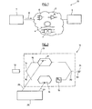
- an optical communication system 10 comprises an optical transmitter 1, an optical receiver 2 and an optical transmission path 3 that links transmitter 1 to receiver 2.
- Optical transmission path 3 may take various forms, e.g. merely an optical fiber 4 or a combination of various optical components in an optical network.
- Optical components that can serve to build a transmission path include e.g. optical amplifiers 5, optical filters or multiplexers 6, optical switches 7 and many others, as will be apparent to those skilled in the art of optical networks.
- optical transmitter 1 To transmit digital data to receiver 3, optical transmitter 1 generates a modulated optical signal 8 in accordance with a modulation method.
- the modulation method imposes 180°-phase transitions or phase jumps on a plurality of optical carrier waves that differ by some property i.e. carrier phase and/or polarization.
- phase jumps can be applied accurately by using a Mach-Zehnder modulator biased at a minimum point of a transfer curve and driven with a driving voltage of twice the switching voltage.
- the QPSK transmitter 11 comprises a continuous wave laser source 12, a QPSK modulator 13 and an optical output 21.
- the QPSK modulator has a well-known structure. It comprises an optical coupler 14 to divide the carrier wave into two carrier wave components in branches 15 and 16, a respective MZM 17 and 18 to modulate the carrier wave component in each branch, a phase shifter 19 to shift the phase of the carrier wave component in one branch by 90° and an optical coupler 20 to superimpose the modulated carrier wave components into the output 21 to form a QPSK-modulated optical signal 22.
- the driving voltages for the MZM 17 and 18 are generated by a baseband signal generator 25 in the form of an NRZ-coded electrical signal 26 and an NRZ-coded electrical signal 27 at a given symbol rate, e.g. 20GHz.
- Baseband signals 26 and 27 are generated in a correlated manner to avoid some symbol transitions that cause strong variations in the intensity of optical signal 22. This will now be explained with reference to Fig. 3 .
- Fig. 3 shows a well-known constellation diagram of a QPSK-modulated signal, which comprises four constellation points representing four symbols 00, 01, 10 and 11.
- baseband signal generator 25 generates baseband signals 26 and 27 so that two diagonally opposed symbols are never generated in a consecutive manner.
- the symbol transitions 30 in the resulting QPSK-modulated optical signal 22 are limited to the four sides of the square and the intensity of the optical signal 22 cannot drop to zero due to any symbol transition.
- the data rate of the modulated signal 22 is lower than in a conventional QPSK modulation which encodes two bits per symbol.
- the modulated signal 22 it is only possible to transmit one and a half bit per symbol by allowing three states at each significant instant, or one bit per symbol by allowing only two states at each significant instant.
- Fig. 4 shows a digital encoder circuit 30 that can be used as a baseband signal generator.
- Digital encoder circuit 30 receives an NZR-coded binary signal X at an electrical input 31 from a source 32 and outputs two correlated NZR-coded binary signals U and V at electrical outputs 34 and 35.
- Digital encoder circuit 30 converts signal X into signals U and V by means of XOR gates 37 and 38, a shift register 39 to generate a 1-bit delayed copy of signal U and an alternating circuit 36 to generate an alternating electrical signal S.
- the alternating signal S has the effect of generating the successive QPSK symbols alternatively in two sub-constellations 41 and 42 of the QPSK constellation of Fig. 3 .
- Table 1 further illustrates the logical operation of Digital encoder circuit 30.
- Table 1 binary signals that may be generated by digital encoder 30. X 0 1 1 1 0 0 1 0 U 0 0 1 0 1 1 1 0 0 S 1 0 1 0 1 0 1 0 1 0 1 V 1 0 0 0 0 1 0 0 1
- signal U can serve as signal 26 and signal V can serve as signal 27.
- An eye diagram of a resulting QPSK-modulated optical signal 22 is shown on Fig. 10 (a) .
- This optical signal has several advantageous properties:
- a conventional NRZ-QPSK-modulated signal takes one of three different intensity levels at each symbol transition, i.e. 0, 1 ⁇ 2 or 1 depending on the data. Therefore, with the encoder circuit 30, a number of different intensity levels has been reduced from 3 to 1 and a maximum intensity variation has been reduced from 100% to 50%.
- the QPSK-modulated optical signal generated with the encoder of Fig. 4 can be demodulated with a conventional QPSK receiver or a coherent receiver with digital signal processing.
- a conventional QPSK receiver or a coherent receiver with digital signal processing As every other QPSK symbol generated with digital encoder circuit 30 belongs to a given subconstellation 41 or 42, it is apparent that signals U and V comprise redundant information.
- This property of the code can be used at the optical receiver 2 for maximum likelihood sequence detection or for transmission error correction.
- Fig. 5 shows another digital encoder circuit 130 that can be used as a baseband signal generator. Elements that are identical to the elements of Fig. 4 are indicated by the same reference numeral. Digital encoder circuit 130 generates signal U by differential encoding of signal X with a 2-bit delay instead of the 1-bit delay in Fig. 4 . Table 2 further illustrates the logical operation of Digital encoder circuit 130. Table 2: binary signals that may be generated by digital encoder 130. X 0 1 1 1 0 0 1 0 U 1 0 1 1 1 0 0 0 0 1 0 S 0 1 0 1 0 1 0 1 0 1 V 1 1 1 0 0 1 0 1 1 1 1 1
- the QPSK-modulated optical signal generated with the encoder of Fig. 5 can be demodulated with a much simpler receiver.
- a suitable receiver 50 is schematically shown on Fig. 6 . It comprises a delay line interferometer 46 with a 2-bit delay in one branch 47 and balanced photodiodes 48.
- the PDM-BPSK transmitter 50 comprises a continuous wave laser source 51, an optical coupler 52 to divide the carrier wave into two carrier wave components in branches 53 and 54, a respective MZM 56 and 57 to modulate the carrier wave component in each branch, and an polarization beam coupler 58 to superimpose a linearly polarized modulated carrier wave component from branch 53 and a linearly polarized modulated carrier wave component from branch 54 into the output 59 to form a PDM-BPSK-modulated optical signal 60.
- the two linearly polarized components are mutually orthogonal.
- the driving voltages for the MZM 56 and 57 are generated by a baseband signal generator 61 in the form of an NRZ-coded electrical signal 63 and an NRZ-coded electrical signal 64 at a given symbol rate, e.g. 20GHz.
- Baseband signals 63 and 64 are generated in a correlated manner to avoid some symbol transitions that cause strong variations in the intensity of optical signal 60.
- the encoder circuits of Figs. 4 and 5 can be used to exclude symbol transitions that make both polarized components drop to zero intensity at the same time.
- the coded PDM-BPSK modulation produces similar benefits to the above-described coded-QPSK modulation, i.e. reduction of non-linear impairments.
- the four significant states of the PDM-BPSK signal 60 could be represented as constellation points in a constellation diagram similar to Fig. 3 .
- Such a constellation diagram has a different meaning however, since each axis would represent a linearly polarized field in that case.
- the PDM-QPSK transmitter 70 comprises a continuous wave laser source 71, an optical coupler 72 to divide the carrier wave into two carrier wave components in branches 73 and 74, a respective QPSK modulator 76 and 77 to modulate the carrier wave component in each branch, and an polarization beam coupler 78 to superimpose a linearly polarized modulated carrier wave component from branch 73 and a linearly polarized modulated carrier wave component from branch 74 into the output 79 to form a PDM-QPSK-modulated optical signal 80.
- the two linearly polarized components are mutually orthogonal.
- the QPSK modulators 76 and 77 can be implemented as the modulator 13 of Fig. 2 .
- the driving voltages for the MZMs of QPSK modulators 76 and 77 are generated by a baseband signal generator 81 in the form of NRZ-coded electrical signals U1, V1, U2 and V2 at a given symbol rate, e.g. 20GHz.
- Baseband signals U1, V1, U2 and V2 are generated in a correlated manner to avoid some symbol transitions that cause strong variations in the intensity of optical signal 60.
- baseband signal generator 81 comprises two encoder circuits which generate the baseband signals for each polarized carrier wave component respectively.
- the encoder circuits of Figs. 4 and 5 can be used to exclude symbol transitions that make the respective polarized component drop to zero intensity.
- baseband signals U1 and V1 can be generated by a first encoder circuit from a first bit stream to be transmitted and baseband signals U1 and V1 can be generated by a second encoder circuit from a second, independent bit stream to be transmitted. Both encoder circuits should operate synchronously to avoid further complexities at the receiver side. Again, this embodiment reduces the intensity variation of the total optical signal to 1 ⁇ 2.
- the baseband signal generator 81 generates all four baseband digital signals in a correlated manner to achieve an even stronger reduction of the intensity variation at symbol transitions.
- the digital encoder circuit 230 shown on Fig. 9 can be used.
- Digital encoder circuit 230 comprises two electrical inputs 83 and 84 to receive two NZR-coded binary signals X and Y from a source 82 and four electrical outputs 85 to produce four correlated NZR-coded binary signals U1, V1, U2 and V2. All signals are coded at a single symbol rate, e.g. 20 GBaud. Signals X and Y comprise the data to be transmitted. Digital encoder circuit 30 converts signals X and Y into signals U1, V1, U2 and V2 by means of multipliers 86, reversers 87, XOR gates 88 and shift registers 90.
- encoder circuit 230 differentially encodes a stream of 2-bit words XY into a stream of 4-bit symbols U1V1 U2V2 in a manner that maps every code value of the incoming words with a single bit transition in the outputted symbols.
- Table 3 operations of digital encoder 230 X 0 1 Y 0 U1 U2 1 V1 V2
- FIG. 10 (b) An eye diagram of a resulting PDM-QPSK-modulated optical signal 60 is shown on Fig. 10 (b) .
- This optical signal has several advantageous properties:
- a conventional NRZ-PDM-QPSK-modulated signal takes one of five different intensity levels at each symbol transition, i.e. 0, 1 ⁇ 4, 1 ⁇ 2, 3 ⁇ 4 or 1 depending on the data. Therefore, with the encoder circuit 230, a number of different intensity levels has been reduced from 5 to 1 and a maximum intensity variation has been reduced from 100% to 25%.
- the PDM-QPSK-modulated optical signal generated with the encoder of Fig. 9 can be demodulated with a coherent receiver with digital signal processing.
- a suitable receiver is shown on Figs. 11 and 12 .
- Figure 11 is a high level functional view of a coherent receiver 100 that includes two coherent mixers 101, four photodiodes 102, four analog to digital converters 103 and a digital signal processor 104.
- Fig. 12 includes a more detailed functional representation of digital signal processor 104.
- the operation of coherent receiver 100 is for the most part known in the art, as disclosed e.g. in EP-A-2086158 .
- an additional decoder module 105 To decode the data encoded with digital encoder circuit 230, an additional decoder module 105 must be inserted after the symbol decision module.
- decoder module 105 reverses the logical mapping shown in table 3 to return the initial bit streams X and Y. Decoder module 105 can also include a maximum likelihood sequence estimator.
- the data sources 32 or 82 can comprise various elements, e.g. digital data storage, high speed memories, FEC coders and others.
- the data to be transmitted at a high clock rate e.g. 20 GHz, 40 GHz or 100 GHz comes from a plurality of tributaries at a lower clock rate, e.g. 10 GHz.
- a parallel-to-serial conversion circuit may be provided in the data source 32 or 82 for that purpose.
- the above embodiments illustrate some modulation methods suitable for optical communications with or without Polarization Division Multiplexing (PDM). It will be apparent to those skilled in the art that these methods can be combined with Wavelength Division Multiplexing (WDM) to improve the transmission capacity of an optical communication system. While the above described embodiments provide various modulation methods, it will be apparent to those skilled in the art that transitions between constellation points can be constrained in a similar manner in many other modulation schemes so as to reduce and/or regularize intensity fluctuations of an optical signal, especially modulation schemes that combine both PSK and amplitude-shift keying (ASK), e.g. Quadrature Amplitude Modulation (QAM).
- PSK PSK
- ASK amplitude-shift keying
- QAM Quadrature Amplitude Modulation
Landscapes
- Engineering & Computer Science (AREA)
- Computer Networks & Wireless Communication (AREA)
- Signal Processing (AREA)
- Physics & Mathematics (AREA)
- Electromagnetism (AREA)
- Optics & Photonics (AREA)
- Optical Communication System (AREA)
Claims (17)
- Procédé de transmission de données sur un canal optique, comprenant les étapes suivantes :générer une pluralité de signaux numériques en bande de base binaires (26, 27, 63, 64, U, V, U1, V1, U2, V2) à un débit de symboles unique pour représenter une séquence de symboles numériques,moduler une pluralité correspondante de composantes d'onde porteuse optique avec la pluralité de signaux numériques en bande de base binaires, la modulation des composantes d'onde porteuse optique étant réalisée avec des modulateurs de Mach-Zehnder (17, 18), de sorte à générer des transitions de phase à 180° de chacune desdites composantes d'onde porteuse optique conformément au signal numérique en bande de base binaire correspondant,et combiner les composantes d'onde porteuse optique modulées dans un milieu de propagation (2),caractérisé en ce que la pluralité de signaux numériques en bande de base binaires sont générés de manière corrélée de sorte qu'au maximum un sous-ensemble des signaux numériques en bande de base binaires effectue une transition de signal entre chaque symbole numérique et le symbole numérique suivant.
- Procédé selon la revendication 1, dans lequel les composantes d'onde porteuse optique comprennent une pluralité de composantes d'onde porteuse optique déphasées présentant une différence de phase prédéterminée.
- Procédé selon la revendication 2, dans lequel la pluralité de composantes d'onde porteuse optique déphasées comprend une composante d'onde porteuse optique en phase et une composante d'onde porteuse optique en quadrature de phase.
- Procédé selon l'une quelconque des revendications 1 à 3, dans lequel les composantes d'onde porteuse optique comprennent une première composante d'onde porteuse optique polarisée et une deuxième composante d'onde porteuse optique polarisée orthogonale à la première composante d'onde porteuse optique polarisée.
- Procédé selon la revendication 1, dans lequel les composantes d'onde porteuse optique comprennent une pluralité de premières composantes d'onde porteuse optique déphasées polarisées présentant une différence de phase prédéterminée et une pluralité de deuxièmes composantes d'onde porteuse optique déphasées polarisées présentant une différence de phase prédéterminée, dans lequel les deuxièmes composantes d'onde porteuse optique déphasées polarisées sont orthogonales aux premières composantes d'onde porteuse optique déphasées polarisées.
- Procédé selon l'une quelconque des revendications 1 à 5, dans lequel un signal numérique en bande de base binaire est codé NRZ, dans lequel la composante d'onde porteuse optique correspondante subit des transitions de phase à 180° conformément à des transitions de signal du signal numérique en bande de base codé NRZ.
- Procédé selon l'une quelconque des revendications 1 à 6, dans lequel au maximum un des signaux numériques en bande de base binaires effectue une transition de signal entre chaque symbole numérique et le symbole numérique suivant.
- Procédé selon l'une quelconque des revendications 1 à 6, dans lequel au moins un des signaux numériques en bande de base binaires effectue une transition de signal entre chaque symbole numérique et le symbole numérique suivant.
- Procédé selon l'une quelconque des revendications 1 à 6, dans lequel un et seulement un des signaux numériques en bande de base binaires effectue une transition de signal entre chaque symbole numérique et le symbole numérique suivant.
- Procédé selon l'une quelconque des revendications 1 à 9, comprenant en outre la conversion d'un flux binaire (X, Y) en la pluralité de signaux numériques en bande de base binaires corrélés (U, V, U1, V1, U2, V2).
- Procédé selon la revendication 10, dans lequel la conversion comprend :le codage différentiel du flux binaire pour générer un premier signal (U) parmi les signaux numériques en bande de base binaires,et le portillonnage OU exclusif du premier signal numérique en bande de base avec un flux binaire alternatif (S) pour générer un deuxième signal (V) parmi les signaux numériques en bande de base binaires.
- Procédé selon la revendication 11, dans lequel le codage différentiel utilise un retard à deux bits.
- Procédé selon l'une quelconque des revendications 1 à 12, dans lequel les modulateurs de Mach-Zehnder (17, 18) sont polarisés à un point minimum d'une courbe de transfert et excités avec une tension d'excitation deux fois égale à la tension de commutation.
- Générateur de signaux en bande de base (25, 61, 81) pour un appareil de modulation optique (13, 50, 70), le générateur de signaux en bande de base comprenant :au moins une entrée électrique (31, 83, 84) pour recevoir au moins un flux binaire,un module de codage numérique (30, 130, 230) pour convertir l'au moins un flux binaire en une pluralité de signaux numériques en bande de base binaires (U, V, U1, V1, U2, V2) à un débit de symboles unique pour représenter une séquence de symboles numériques, une pluralité de sorties électriques (34, 35, 85) permettant de délivrer la pluralité de signaux numériques en bande de base binaires à une pluralité correspondante de modulateurs optiques de Mach-Zehnder (17, 18, 56, 57, 76, 77) pour générer des transitions de phase à 180° de composantes d'onde porteuse optique conformément aux signaux numériques en bande de base binaires,caractérisé en ce que le module de codage numérique peut générer la pluralité de signaux numériques en bande de base binaires de manière corrélée, de sorte qu'au maximum un sous-ensemble des signaux numériques en bande de base binaires effectue une transition de signal entre chaque symbole numérique et le symbole numérique suivant de la séquence.
- Générateur de signaux en bande de base selon la revendication 14, dans lequel le module de codage numérique comprend :un codeur différentiel (37, 39) pour coder de manière différentielle le flux binaire afin de générer un premier signal (U) parmi les signaux numériques en bande de base binaires,un circuit alternatif (36) pour générer un flux binaire alternatif au débit de symboles unique,et une porte OU exclusif (38) pour combiner le premier signal numérique en bande de base binaire avec le flux binaire alternatif pour générer un deuxième signal (V) parmi les signaux numériques en bande de base binaires.
- Générateur de signaux en bande de base selon la revendication 14 ou 15, dans lequel l'au moins un flux binaire (X, Y) représente une séquence de mots numériques, dans lequel le module de codage numérique (30, 230) peut associer de manière unique chaque valeur de code desdits mots numériques à un signal correspondant parmi les signaux numériques en bande de base binaires (U, V, U1, V1, U2, V2), dans lequel pour chaque mot numérique reçu présentant une valeur de code, le module de codage numérique génère une transition de signal du signal numérique en bande de base binaire correspondant à ladite valeur de code et génère le reste des signaux numériques en bande de base binaires pour rester constant.
- Générateur de signaux en bande de base selon l'une quelconque des revendications 14 à 16, dans lequel le module de codage numérique (30, 130, 230) peut convertir une séquence de mots numériques à n bits à un débit de symboles unique en une séquence de symboles numériques à 2" bits au débit de symboles unique, n étant un nombre entier positif.
Priority Applications (3)
| Application Number | Priority Date | Filing Date | Title |
|---|---|---|---|
| EP20100305008 EP2341642B1 (fr) | 2010-01-05 | 2010-01-05 | Procédé de transmission de données dans un canal optique |
| PCT/EP2010/069894 WO2011083015A1 (fr) | 2010-01-05 | 2010-12-16 | Procédé pour transmettre des données sur un canal optique |
| TW99144757A TW201145857A (en) | 2010-01-05 | 2010-12-20 | Method for transmitting data on an optical channel |
Applications Claiming Priority (1)
| Application Number | Priority Date | Filing Date | Title |
|---|---|---|---|
| EP20100305008 EP2341642B1 (fr) | 2010-01-05 | 2010-01-05 | Procédé de transmission de données dans un canal optique |
Publications (2)
| Publication Number | Publication Date |
|---|---|
| EP2341642A1 EP2341642A1 (fr) | 2011-07-06 |
| EP2341642B1 true EP2341642B1 (fr) | 2015-05-20 |
Family
ID=42194764
Family Applications (1)
| Application Number | Title | Priority Date | Filing Date |
|---|---|---|---|
| EP20100305008 Not-in-force EP2341642B1 (fr) | 2010-01-05 | 2010-01-05 | Procédé de transmission de données dans un canal optique |
Country Status (3)
| Country | Link |
|---|---|
| EP (1) | EP2341642B1 (fr) |
| TW (1) | TW201145857A (fr) |
| WO (1) | WO2011083015A1 (fr) |
Families Citing this family (2)
| Publication number | Priority date | Publication date | Assignee | Title |
|---|---|---|---|---|
| US8625936B1 (en) * | 2012-06-29 | 2014-01-07 | Alcatel Lucent | Advanced modulation formats using optical modulators |
| EP3959833B1 (fr) * | 2019-04-25 | 2024-12-04 | Sew-Eurodrive GmbH & Co. KG | Procédé de transmission de données entre un premier et un second module et système comportant des parties mobiles permettant d'exécuter le procédé |
Family Cites Families (5)
| Publication number | Priority date | Publication date | Assignee | Title |
|---|---|---|---|---|
| US7412008B2 (en) * | 2003-06-30 | 2008-08-12 | Freescale Semiconductor, Inc. | Programmable phase mapping and phase rotation modulator and method |
| US7688911B2 (en) * | 2006-03-28 | 2010-03-30 | Teledyne Licensing, L.L.C. | Method and apparatus for synchronizing alternating quadratures differential binary phase shift keying modulation and demodulation arrangements |
| EP2086158B1 (fr) | 2008-01-29 | 2011-06-22 | Alcatel Lucent | Schéma de récupération d'horloge pour un récepteur optique basé sur la surveillance du précurseur et postcurseur des coefficients de prise |
| EP2109233B1 (fr) * | 2008-04-11 | 2010-08-04 | Alcatel Lucent | Schéma de modulation doté d'un nombre supérieur d'états de polarisation |
| US8155534B2 (en) * | 2008-06-30 | 2012-04-10 | Alcatel Lucent | Optical modulator for higher-order modulation |
-
2010
- 2010-01-05 EP EP20100305008 patent/EP2341642B1/fr not_active Not-in-force
- 2010-12-16 WO PCT/EP2010/069894 patent/WO2011083015A1/fr not_active Ceased
- 2010-12-20 TW TW99144757A patent/TW201145857A/zh unknown
Also Published As
| Publication number | Publication date |
|---|---|
| WO2011083015A1 (fr) | 2011-07-14 |
| EP2341642A1 (fr) | 2011-07-06 |
| TW201145857A (en) | 2011-12-16 |
Similar Documents
| Publication | Publication Date | Title |
|---|---|---|
| US11902079B2 (en) | Distribution matching for probabilistic constellation shaping with an arbitrary input/output alphabet | |
| EP3469743B1 (fr) | Procédé de codage de données optiques et émetteur optique | |
| EP3107255B1 (fr) | Formats de modulation optique avec une tolérance augmentée à des non-linéarités et à haute efficacité spectrale | |
| US11038596B2 (en) | Nonlinear tolerant super-Gaussian distribution for probabilistic shaping modulation | |
| US8719656B2 (en) | Four-dimensional non-binary LDPC-coded modulation schemes for ultra high-speed optical fiber communication | |
| WO2016121341A1 (fr) | Émetteur optique, système de communication optique, et procédé de communication optique | |
| JP2004170954A (ja) | 光位相多値変調方法と光位相多値変調装置および誤り制御方法 | |
| EP2341642B1 (fr) | Procédé de transmission de données dans un canal optique | |
| US9998229B2 (en) | Optimized star-8QAM performance for binary encoding | |
| CN111181651A (zh) | 一种提高传输速率的四维编码调制系统 | |
| US11476943B2 (en) | Optical transmitter, optical communication system, and optical communication method | |
| JP5478336B2 (ja) | 光伝送方法、光伝送システム、光送信機、光受信機 | |
| JP2008167126A (ja) | 光ディジタル伝送システムおよび方法 | |
| US20250260494A1 (en) | Distribution matrching for probabilistic constellation shaping with an arbitrary input/ouput alphabet | |
| Alvarado et al. | Achievable rates for four-dimensional coded modulation with a bit-wise receiver | |
| CN101478347A (zh) | 无反馈回路的光差分正交移相键控调制器的预编码器 | |
| JP2007288591A (ja) | 光直交振幅変調回路および光送信器 | |
| JP5161330B2 (ja) | 光直交振幅変調回路および光送信器 | |
| US12126483B2 (en) | Bits-to-symbols mapping for amplitude modulation | |
| US12107633B2 (en) | Two-dimensional optical modulation and detection technologies for optical communications | |
| Leoni et al. | Constellation expansion for differentially encoded 100G transmission | |
| US8502711B2 (en) | Swap tolerant coding and decoding circuits and methods | |
| JP5161329B2 (ja) | 光送信器および光直交振幅変調方法 | |
| HK40104423A (zh) | 用於光通信的二维光调制和检测技术 | |
| CN120835029A (zh) | 光信号发送和接收方法、光通信装置和系统、设备及介质 |
Legal Events
| Date | Code | Title | Description |
|---|---|---|---|
| PUAI | Public reference made under article 153(3) epc to a published international application that has entered the european phase |
Free format text: ORIGINAL CODE: 0009012 |
|
| AK | Designated contracting states |
Kind code of ref document: A1 Designated state(s): AT BE BG CH CY CZ DE DK EE ES FI FR GB GR HR HU IE IS IT LI LT LU LV MC MK MT NL NO PL PT RO SE SI SK SM TR |
|
| AX | Request for extension of the european patent |
Extension state: AL BA RS |
|
| 17P | Request for examination filed |
Effective date: 20120109 |
|
| RAP1 | Party data changed (applicant data changed or rights of an application transferred) |
Owner name: ALCATEL LUCENT |
|
| 111Z | Information provided on other rights and legal means of execution |
Free format text: AT BE BG CH CY CZ DE DK EE ES FI FR GB GR HR HU IE IS IT LI LT LU LV MC MK MT NL NO PL PT RO SE SI SK SM TR Effective date: 20130410 |
|
| 17Q | First examination report despatched |
Effective date: 20131007 |
|
| RAP1 | Party data changed (applicant data changed or rights of an application transferred) |
Owner name: ALCATEL LUCENT |
|
| D11X | Information provided on other rights and legal means of execution (deleted) | ||
| REG | Reference to a national code |
Ref country code: DE Ref legal event code: R079 Ref document number: 602010024729 Country of ref document: DE Free format text: PREVIOUS MAIN CLASS: H04B0010155000 Ipc: H04B0010500000 |
|
| RIC1 | Information provided on ipc code assigned before grant |
Ipc: H04L 27/20 20060101ALI20141204BHEP Ipc: H04B 10/556 20130101ALI20141204BHEP Ipc: H04B 10/50 20130101AFI20141204BHEP |
|
| GRAP | Despatch of communication of intention to grant a patent |
Free format text: ORIGINAL CODE: EPIDOSNIGR1 |
|
| INTG | Intention to grant announced |
Effective date: 20150113 |
|
| GRAS | Grant fee paid |
Free format text: ORIGINAL CODE: EPIDOSNIGR3 |
|
| GRAA | (expected) grant |
Free format text: ORIGINAL CODE: 0009210 |
|
| AK | Designated contracting states |
Kind code of ref document: B1 Designated state(s): AT BE BG CH CY CZ DE DK EE ES FI FR GB GR HR HU IE IS IT LI LT LU LV MC MK MT NL NO PL PT RO SE SI SK SM TR |
|
| REG | Reference to a national code |
Ref country code: GB Ref legal event code: FG4D |
|
| REG | Reference to a national code |
Ref country code: CH Ref legal event code: EP |
|
| REG | Reference to a national code |
Ref country code: AT Ref legal event code: REF Ref document number: 728211 Country of ref document: AT Kind code of ref document: T Effective date: 20150615 |
|
| REG | Reference to a national code |
Ref country code: IE Ref legal event code: FG4D |
|
| REG | Reference to a national code |
Ref country code: DE Ref legal event code: R096 Ref document number: 602010024729 Country of ref document: DE Effective date: 20150625 |
|
| REG | Reference to a national code |
Ref country code: AT Ref legal event code: MK05 Ref document number: 728211 Country of ref document: AT Kind code of ref document: T Effective date: 20150520 |
|
| REG | Reference to a national code |
Ref country code: LT Ref legal event code: MG4D |
|
| REG | Reference to a national code |
Ref country code: NL Ref legal event code: MP Effective date: 20150520 |
|
| PG25 | Lapsed in a contracting state [announced via postgrant information from national office to epo] |
Ref country code: PT Free format text: LAPSE BECAUSE OF FAILURE TO SUBMIT A TRANSLATION OF THE DESCRIPTION OR TO PAY THE FEE WITHIN THE PRESCRIBED TIME-LIMIT Effective date: 20150921 Ref country code: LT Free format text: LAPSE BECAUSE OF FAILURE TO SUBMIT A TRANSLATION OF THE DESCRIPTION OR TO PAY THE FEE WITHIN THE PRESCRIBED TIME-LIMIT Effective date: 20150520 Ref country code: ES Free format text: LAPSE BECAUSE OF FAILURE TO SUBMIT A TRANSLATION OF THE DESCRIPTION OR TO PAY THE FEE WITHIN THE PRESCRIBED TIME-LIMIT Effective date: 20150520 Ref country code: FI Free format text: LAPSE BECAUSE OF FAILURE TO SUBMIT A TRANSLATION OF THE DESCRIPTION OR TO PAY THE FEE WITHIN THE PRESCRIBED TIME-LIMIT Effective date: 20150520 Ref country code: NO Free format text: LAPSE BECAUSE OF FAILURE TO SUBMIT A TRANSLATION OF THE DESCRIPTION OR TO PAY THE FEE WITHIN THE PRESCRIBED TIME-LIMIT Effective date: 20150820 Ref country code: HR Free format text: LAPSE BECAUSE OF FAILURE TO SUBMIT A TRANSLATION OF THE DESCRIPTION OR TO PAY THE FEE WITHIN THE PRESCRIBED TIME-LIMIT Effective date: 20150520 |
|
| PG25 | Lapsed in a contracting state [announced via postgrant information from national office to epo] |
Ref country code: LV Free format text: LAPSE BECAUSE OF FAILURE TO SUBMIT A TRANSLATION OF THE DESCRIPTION OR TO PAY THE FEE WITHIN THE PRESCRIBED TIME-LIMIT Effective date: 20150520 Ref country code: BG Free format text: LAPSE BECAUSE OF FAILURE TO SUBMIT A TRANSLATION OF THE DESCRIPTION OR TO PAY THE FEE WITHIN THE PRESCRIBED TIME-LIMIT Effective date: 20150820 Ref country code: GR Free format text: LAPSE BECAUSE OF FAILURE TO SUBMIT A TRANSLATION OF THE DESCRIPTION OR TO PAY THE FEE WITHIN THE PRESCRIBED TIME-LIMIT Effective date: 20150821 Ref country code: AT Free format text: LAPSE BECAUSE OF FAILURE TO SUBMIT A TRANSLATION OF THE DESCRIPTION OR TO PAY THE FEE WITHIN THE PRESCRIBED TIME-LIMIT Effective date: 20150520 Ref country code: IS Free format text: LAPSE BECAUSE OF FAILURE TO SUBMIT A TRANSLATION OF THE DESCRIPTION OR TO PAY THE FEE WITHIN THE PRESCRIBED TIME-LIMIT Effective date: 20150920 |
|
| REG | Reference to a national code |
Ref country code: FR Ref legal event code: PLFP Year of fee payment: 7 |
|
| PG25 | Lapsed in a contracting state [announced via postgrant information from national office to epo] |
Ref country code: DK Free format text: LAPSE BECAUSE OF FAILURE TO SUBMIT A TRANSLATION OF THE DESCRIPTION OR TO PAY THE FEE WITHIN THE PRESCRIBED TIME-LIMIT Effective date: 20150520 Ref country code: EE Free format text: LAPSE BECAUSE OF FAILURE TO SUBMIT A TRANSLATION OF THE DESCRIPTION OR TO PAY THE FEE WITHIN THE PRESCRIBED TIME-LIMIT Effective date: 20150520 |
|
| REG | Reference to a national code |
Ref country code: DE Ref legal event code: R097 Ref document number: 602010024729 Country of ref document: DE |
|
| PG25 | Lapsed in a contracting state [announced via postgrant information from national office to epo] |
Ref country code: PL Free format text: LAPSE BECAUSE OF FAILURE TO SUBMIT A TRANSLATION OF THE DESCRIPTION OR TO PAY THE FEE WITHIN THE PRESCRIBED TIME-LIMIT Effective date: 20150520 Ref country code: SK Free format text: LAPSE BECAUSE OF FAILURE TO SUBMIT A TRANSLATION OF THE DESCRIPTION OR TO PAY THE FEE WITHIN THE PRESCRIBED TIME-LIMIT Effective date: 20150520 Ref country code: CZ Free format text: LAPSE BECAUSE OF FAILURE TO SUBMIT A TRANSLATION OF THE DESCRIPTION OR TO PAY THE FEE WITHIN THE PRESCRIBED TIME-LIMIT Effective date: 20150520 Ref country code: RO Free format text: LAPSE BECAUSE OF NON-PAYMENT OF DUE FEES Effective date: 20150520 |
|
| PLBE | No opposition filed within time limit |
Free format text: ORIGINAL CODE: 0009261 |
|
| STAA | Information on the status of an ep patent application or granted ep patent |
Free format text: STATUS: NO OPPOSITION FILED WITHIN TIME LIMIT |
|
| 26N | No opposition filed |
Effective date: 20160223 |
|
| PG25 | Lapsed in a contracting state [announced via postgrant information from national office to epo] |
Ref country code: IT Free format text: LAPSE BECAUSE OF FAILURE TO SUBMIT A TRANSLATION OF THE DESCRIPTION OR TO PAY THE FEE WITHIN THE PRESCRIBED TIME-LIMIT Effective date: 20150520 |
|
| PG25 | Lapsed in a contracting state [announced via postgrant information from national office to epo] |
Ref country code: SI Free format text: LAPSE BECAUSE OF FAILURE TO SUBMIT A TRANSLATION OF THE DESCRIPTION OR TO PAY THE FEE WITHIN THE PRESCRIBED TIME-LIMIT Effective date: 20150520 Ref country code: BE Free format text: LAPSE BECAUSE OF NON-PAYMENT OF DUE FEES Effective date: 20160131 |
|
| PG25 | Lapsed in a contracting state [announced via postgrant information from national office to epo] |
Ref country code: LU Free format text: LAPSE BECAUSE OF FAILURE TO SUBMIT A TRANSLATION OF THE DESCRIPTION OR TO PAY THE FEE WITHIN THE PRESCRIBED TIME-LIMIT Effective date: 20160105 Ref country code: BE Free format text: LAPSE BECAUSE OF FAILURE TO SUBMIT A TRANSLATION OF THE DESCRIPTION OR TO PAY THE FEE WITHIN THE PRESCRIBED TIME-LIMIT Effective date: 20150520 |
|
| REG | Reference to a national code |
Ref country code: CH Ref legal event code: PL |
|
| PG25 | Lapsed in a contracting state [announced via postgrant information from national office to epo] |
Ref country code: MC Free format text: LAPSE BECAUSE OF FAILURE TO SUBMIT A TRANSLATION OF THE DESCRIPTION OR TO PAY THE FEE WITHIN THE PRESCRIBED TIME-LIMIT Effective date: 20150520 |
|
| PG25 | Lapsed in a contracting state [announced via postgrant information from national office to epo] |
Ref country code: LI Free format text: LAPSE BECAUSE OF NON-PAYMENT OF DUE FEES Effective date: 20160131 Ref country code: CH Free format text: LAPSE BECAUSE OF NON-PAYMENT OF DUE FEES Effective date: 20160131 |
|
| REG | Reference to a national code |
Ref country code: IE Ref legal event code: MM4A |
|
| REG | Reference to a national code |
Ref country code: FR Ref legal event code: PLFP Year of fee payment: 8 |
|
| PG25 | Lapsed in a contracting state [announced via postgrant information from national office to epo] |
Ref country code: IE Free format text: LAPSE BECAUSE OF NON-PAYMENT OF DUE FEES Effective date: 20160105 |
|
| PGFP | Annual fee paid to national office [announced via postgrant information from national office to epo] |
Ref country code: FR Payment date: 20170120 Year of fee payment: 8 Ref country code: DE Payment date: 20170120 Year of fee payment: 8 |
|
| PGFP | Annual fee paid to national office [announced via postgrant information from national office to epo] |
Ref country code: GB Payment date: 20170119 Year of fee payment: 8 |
|
| PG25 | Lapsed in a contracting state [announced via postgrant information from national office to epo] |
Ref country code: SE Free format text: LAPSE BECAUSE OF FAILURE TO SUBMIT A TRANSLATION OF THE DESCRIPTION OR TO PAY THE FEE WITHIN THE PRESCRIBED TIME-LIMIT Effective date: 20150520 Ref country code: NL Free format text: LAPSE BECAUSE OF FAILURE TO SUBMIT A TRANSLATION OF THE DESCRIPTION OR TO PAY THE FEE WITHIN THE PRESCRIBED TIME-LIMIT Effective date: 20150520 |
|
| PG25 | Lapsed in a contracting state [announced via postgrant information from national office to epo] |
Ref country code: MT Free format text: LAPSE BECAUSE OF FAILURE TO SUBMIT A TRANSLATION OF THE DESCRIPTION OR TO PAY THE FEE WITHIN THE PRESCRIBED TIME-LIMIT Effective date: 20150520 |
|
| PG25 | Lapsed in a contracting state [announced via postgrant information from national office to epo] |
Ref country code: SM Free format text: LAPSE BECAUSE OF FAILURE TO SUBMIT A TRANSLATION OF THE DESCRIPTION OR TO PAY THE FEE WITHIN THE PRESCRIBED TIME-LIMIT Effective date: 20150520 Ref country code: CY Free format text: LAPSE BECAUSE OF FAILURE TO SUBMIT A TRANSLATION OF THE DESCRIPTION OR TO PAY THE FEE WITHIN THE PRESCRIBED TIME-LIMIT Effective date: 20150520 Ref country code: HU Free format text: LAPSE BECAUSE OF FAILURE TO SUBMIT A TRANSLATION OF THE DESCRIPTION OR TO PAY THE FEE WITHIN THE PRESCRIBED TIME-LIMIT; INVALID AB INITIO Effective date: 20100105 |
|
| PG25 | Lapsed in a contracting state [announced via postgrant information from national office to epo] |
Ref country code: MT Free format text: LAPSE BECAUSE OF FAILURE TO SUBMIT A TRANSLATION OF THE DESCRIPTION OR TO PAY THE FEE WITHIN THE PRESCRIBED TIME-LIMIT Effective date: 20160131 Ref country code: MK Free format text: LAPSE BECAUSE OF FAILURE TO SUBMIT A TRANSLATION OF THE DESCRIPTION OR TO PAY THE FEE WITHIN THE PRESCRIBED TIME-LIMIT Effective date: 20150520 Ref country code: TR Free format text: LAPSE BECAUSE OF FAILURE TO SUBMIT A TRANSLATION OF THE DESCRIPTION OR TO PAY THE FEE WITHIN THE PRESCRIBED TIME-LIMIT Effective date: 20150520 |
|
| REG | Reference to a national code |
Ref country code: DE Ref legal event code: R119 Ref document number: 602010024729 Country of ref document: DE |
|
| GBPC | Gb: european patent ceased through non-payment of renewal fee |
Effective date: 20180105 |
|
| PG25 | Lapsed in a contracting state [announced via postgrant information from national office to epo] |
Ref country code: FR Free format text: LAPSE BECAUSE OF NON-PAYMENT OF DUE FEES Effective date: 20180131 Ref country code: DE Free format text: LAPSE BECAUSE OF NON-PAYMENT OF DUE FEES Effective date: 20180801 |
|
| REG | Reference to a national code |
Ref country code: FR Ref legal event code: ST Effective date: 20180928 |
|
| PG25 | Lapsed in a contracting state [announced via postgrant information from national office to epo] |
Ref country code: GB Free format text: LAPSE BECAUSE OF NON-PAYMENT OF DUE FEES Effective date: 20180105 |