EP2346094A1 - Procédé de fabrication d'un détecteur de rayonnements - Google Patents
Procédé de fabrication d'un détecteur de rayonnements Download PDFInfo
- Publication number
- EP2346094A1 EP2346094A1 EP10150660A EP10150660A EP2346094A1 EP 2346094 A1 EP2346094 A1 EP 2346094A1 EP 10150660 A EP10150660 A EP 10150660A EP 10150660 A EP10150660 A EP 10150660A EP 2346094 A1 EP2346094 A1 EP 2346094A1
- Authority
- EP
- European Patent Office
- Prior art keywords
- layer
- boron
- detector
- grid
- radiation
- Prior art date
- Legal status (The legal status is an assumption and is not a legal conclusion. Google has not performed a legal analysis and makes no representation as to the accuracy of the status listed.)
- Withdrawn
Links
- 230000005855 radiation Effects 0.000 title claims abstract description 62
- 238000004519 manufacturing process Methods 0.000 title claims abstract description 9
- 229910052796 boron Inorganic materials 0.000 claims abstract description 124
- ZOXJGFHDIHLPTG-UHFFFAOYSA-N Boron Chemical group [B] ZOXJGFHDIHLPTG-UHFFFAOYSA-N 0.000 claims abstract description 123
- 238000000034 method Methods 0.000 claims abstract description 38
- 229910052782 aluminium Inorganic materials 0.000 claims abstract description 33
- 238000005530 etching Methods 0.000 claims abstract description 23
- 238000001039 wet etching Methods 0.000 claims abstract description 22
- 238000001312 dry etching Methods 0.000 claims abstract description 19
- 238000009792 diffusion process Methods 0.000 claims abstract description 15
- 239000010410 layer Substances 0.000 claims description 224
- 239000000758 substrate Substances 0.000 claims description 46
- 239000011241 protective layer Substances 0.000 claims description 29
- 239000002245 particle Substances 0.000 claims description 21
- 239000004020 conductor Substances 0.000 claims description 20
- 239000000463 material Substances 0.000 claims description 18
- JKWMSGQKBLHBQQ-UHFFFAOYSA-N diboron trioxide Chemical compound O=BOB=O JKWMSGQKBLHBQQ-UHFFFAOYSA-N 0.000 claims description 7
- 229910052580 B4C Inorganic materials 0.000 claims description 6
- 229910052582 BN Inorganic materials 0.000 claims description 6
- PZNSFCLAULLKQX-UHFFFAOYSA-N Boron nitride Chemical compound N#B PZNSFCLAULLKQX-UHFFFAOYSA-N 0.000 claims description 6
- INAHAJYZKVIDIZ-UHFFFAOYSA-N boron carbide Chemical compound B12B3B4C32B41 INAHAJYZKVIDIZ-UHFFFAOYSA-N 0.000 claims description 6
- 229910052810 boron oxide Inorganic materials 0.000 claims description 6
- 150000002500 ions Chemical class 0.000 claims description 5
- 239000000203 mixture Substances 0.000 claims description 5
- ATJFFYVFTNAWJD-UHFFFAOYSA-N Tin Chemical compound [Sn] ATJFFYVFTNAWJD-UHFFFAOYSA-N 0.000 claims description 4
- 229910052804 chromium Inorganic materials 0.000 claims description 4
- 229910052802 copper Inorganic materials 0.000 claims description 4
- 238000000151 deposition Methods 0.000 claims description 4
- 229910052737 gold Inorganic materials 0.000 claims description 4
- 229910052750 molybdenum Inorganic materials 0.000 claims description 4
- 229910052759 nickel Inorganic materials 0.000 claims description 4
- 229910052763 palladium Inorganic materials 0.000 claims description 4
- 229910052697 platinum Inorganic materials 0.000 claims description 4
- 229910052721 tungsten Inorganic materials 0.000 claims description 4
- 239000002019 doping agent Substances 0.000 claims description 3
- 238000010884 ion-beam technique Methods 0.000 claims description 3
- 239000004411 aluminium Substances 0.000 abstract description 29
- XAGFODPZIPBFFR-UHFFFAOYSA-N aluminium Chemical compound [Al] XAGFODPZIPBFFR-UHFFFAOYSA-N 0.000 abstract description 29
- 230000008569 process Effects 0.000 abstract description 14
- VYPSYNLAJGMNEJ-UHFFFAOYSA-N Silicium dioxide Chemical compound O=[Si]=O VYPSYNLAJGMNEJ-UHFFFAOYSA-N 0.000 description 12
- XUIMIQQOPSSXEZ-UHFFFAOYSA-N Silicon Chemical compound [Si] XUIMIQQOPSSXEZ-UHFFFAOYSA-N 0.000 description 9
- 229910052710 silicon Inorganic materials 0.000 description 9
- 239000010703 silicon Substances 0.000 description 9
- 230000035515 penetration Effects 0.000 description 8
- 235000012431 wafers Nutrition 0.000 description 7
- 230000000694 effects Effects 0.000 description 6
- 239000000377 silicon dioxide Substances 0.000 description 6
- 229910052681 coesite Inorganic materials 0.000 description 5
- 229910052906 cristobalite Inorganic materials 0.000 description 5
- 238000001514 detection method Methods 0.000 description 5
- 239000004065 semiconductor Substances 0.000 description 5
- 229910052682 stishovite Inorganic materials 0.000 description 5
- 229910052905 tridymite Inorganic materials 0.000 description 5
- OKTJSMMVPCPJKN-UHFFFAOYSA-N Carbon Chemical compound [C] OKTJSMMVPCPJKN-UHFFFAOYSA-N 0.000 description 4
- 150000001639 boron compounds Chemical class 0.000 description 4
- 229910052799 carbon Inorganic materials 0.000 description 4
- 238000004140 cleaning Methods 0.000 description 4
- 238000012545 processing Methods 0.000 description 4
- 230000005540 biological transmission Effects 0.000 description 3
- 238000010894 electron beam technology Methods 0.000 description 3
- IJGRMHOSHXDMSA-UHFFFAOYSA-N Atomic nitrogen Chemical compound N#N IJGRMHOSHXDMSA-UHFFFAOYSA-N 0.000 description 2
- 229910001218 Gallium arsenide Inorganic materials 0.000 description 2
- 201000009310 astigmatism Diseases 0.000 description 2
- 239000003990 capacitor Substances 0.000 description 2
- 238000011109 contamination Methods 0.000 description 2
- 229910052732 germanium Inorganic materials 0.000 description 2
- GNPVGFCGXDBREM-UHFFFAOYSA-N germanium atom Chemical compound [Ge] GNPVGFCGXDBREM-UHFFFAOYSA-N 0.000 description 2
- 238000003384 imaging method Methods 0.000 description 2
- 239000007943 implant Substances 0.000 description 2
- 238000011835 investigation Methods 0.000 description 2
- 238000002955 isolation Methods 0.000 description 2
- 238000001465 metallisation Methods 0.000 description 2
- 230000005405 multipole Effects 0.000 description 2
- 230000003287 optical effect Effects 0.000 description 2
- 238000001020 plasma etching Methods 0.000 description 2
- 230000001681 protective effect Effects 0.000 description 2
- 230000004044 response Effects 0.000 description 2
- 238000001350 scanning transmission electron microscopy Methods 0.000 description 2
- 238000011896 sensitive detection Methods 0.000 description 2
- 239000007787 solid Substances 0.000 description 2
- 239000000126 substance Substances 0.000 description 2
- UFHFLCQGNIYNRP-UHFFFAOYSA-N Hydrogen Chemical compound [H][H] UFHFLCQGNIYNRP-UHFFFAOYSA-N 0.000 description 1
- OAICVXFJPJFONN-UHFFFAOYSA-N Phosphorus Chemical compound [P] OAICVXFJPJFONN-UHFFFAOYSA-N 0.000 description 1
- 238000010521 absorption reaction Methods 0.000 description 1
- 238000004458 analytical method Methods 0.000 description 1
- QVGXLLKOCUKJST-UHFFFAOYSA-N atomic oxygen Chemical compound [O] QVGXLLKOCUKJST-UHFFFAOYSA-N 0.000 description 1
- 230000004888 barrier function Effects 0.000 description 1
- 230000009286 beneficial effect Effects 0.000 description 1
- 230000008901 benefit Effects 0.000 description 1
- 150000001638 boron Chemical class 0.000 description 1
- 238000005136 cathodoluminescence Methods 0.000 description 1
- 238000004040 coloring Methods 0.000 description 1
- 230000001419 dependent effect Effects 0.000 description 1
- 230000008021 deposition Effects 0.000 description 1
- 238000013461 design Methods 0.000 description 1
- 230000023077 detection of light stimulus Effects 0.000 description 1
- 239000003989 dielectric material Substances 0.000 description 1
- 238000007598 dipping method Methods 0.000 description 1
- 230000009977 dual effect Effects 0.000 description 1
- 230000005684 electric field Effects 0.000 description 1
- 230000005670 electromagnetic radiation Effects 0.000 description 1
- 238000005516 engineering process Methods 0.000 description 1
- 230000002708 enhancing effect Effects 0.000 description 1
- 230000007613 environmental effect Effects 0.000 description 1
- 238000002474 experimental method Methods 0.000 description 1
- -1 formed on it Substances 0.000 description 1
- 229910052739 hydrogen Inorganic materials 0.000 description 1
- 239000001257 hydrogen Substances 0.000 description 1
- 239000012535 impurity Substances 0.000 description 1
- 239000012212 insulator Substances 0.000 description 1
- 230000010354 integration Effects 0.000 description 1
- 238000010849 ion bombardment Methods 0.000 description 1
- 238000003754 machining Methods 0.000 description 1
- 229910052751 metal Inorganic materials 0.000 description 1
- 239000002184 metal Substances 0.000 description 1
- 229910052757 nitrogen Inorganic materials 0.000 description 1
- 229910052760 oxygen Inorganic materials 0.000 description 1
- 239000001301 oxygen Substances 0.000 description 1
- 229910052698 phosphorus Inorganic materials 0.000 description 1
- 239000011574 phosphorus Substances 0.000 description 1
- 239000002243 precursor Substances 0.000 description 1
- 230000009467 reduction Effects 0.000 description 1
- 239000011163 secondary particle Substances 0.000 description 1
- 235000012239 silicon dioxide Nutrition 0.000 description 1
- 239000002344 surface layer Substances 0.000 description 1
- 238000010408 sweeping Methods 0.000 description 1
- 238000012876 topography Methods 0.000 description 1
Images

Classifications
-
- H—ELECTRICITY
- H10—SEMICONDUCTOR DEVICES; ELECTRIC SOLID-STATE DEVICES NOT OTHERWISE PROVIDED FOR
- H10F—INORGANIC SEMICONDUCTOR DEVICES SENSITIVE TO INFRARED RADIATION, LIGHT, ELECTROMAGNETIC RADIATION OF SHORTER WAVELENGTH OR CORPUSCULAR RADIATION
- H10F30/00—Individual radiation-sensitive semiconductor devices in which radiation controls the flow of current through the devices, e.g. photodetectors
- H10F30/20—Individual radiation-sensitive semiconductor devices in which radiation controls the flow of current through the devices, e.g. photodetectors the devices having potential barriers, e.g. phototransistors
- H10F30/29—Individual radiation-sensitive semiconductor devices in which radiation controls the flow of current through the devices, e.g. photodetectors the devices having potential barriers, e.g. phototransistors the devices being sensitive to radiation having very short wavelengths, e.g. X-rays, gamma-rays or corpuscular radiation
- H10F30/295—Surface barrier or shallow PN junction radiation detectors, e.g. surface barrier alpha-particle detectors
- H10F30/2955—Shallow PN junction radiation detectors
-
- H—ELECTRICITY
- H01—ELECTRIC ELEMENTS
- H01J—ELECTRIC DISCHARGE TUBES OR DISCHARGE LAMPS
- H01J37/00—Discharge tubes with provision for introducing objects or material to be exposed to the discharge, e.g. for the purpose of examination or processing thereof
- H01J37/02—Details
- H01J37/244—Detectors; Associated components or circuits therefor
-
- H—ELECTRICITY
- H10—SEMICONDUCTOR DEVICES; ELECTRIC SOLID-STATE DEVICES NOT OTHERWISE PROVIDED FOR
- H10F—INORGANIC SEMICONDUCTOR DEVICES SENSITIVE TO INFRARED RADIATION, LIGHT, ELECTROMAGNETIC RADIATION OF SHORTER WAVELENGTH OR CORPUSCULAR RADIATION
- H10F30/00—Individual radiation-sensitive semiconductor devices in which radiation controls the flow of current through the devices, e.g. photodetectors
- H10F30/20—Individual radiation-sensitive semiconductor devices in which radiation controls the flow of current through the devices, e.g. photodetectors the devices having potential barriers, e.g. phototransistors
- H10F30/21—Individual radiation-sensitive semiconductor devices in which radiation controls the flow of current through the devices, e.g. photodetectors the devices having potential barriers, e.g. phototransistors the devices being sensitive to infrared, visible or ultraviolet radiation
- H10F30/22—Individual radiation-sensitive semiconductor devices in which radiation controls the flow of current through the devices, e.g. photodetectors the devices having potential barriers, e.g. phototransistors the devices being sensitive to infrared, visible or ultraviolet radiation the devices having only one potential barrier, e.g. photodiodes
- H10F30/223—Individual radiation-sensitive semiconductor devices in which radiation controls the flow of current through the devices, e.g. photodetectors the devices having potential barriers, e.g. phototransistors the devices being sensitive to infrared, visible or ultraviolet radiation the devices having only one potential barrier, e.g. photodiodes the potential barrier being a PIN barrier
-
- H—ELECTRICITY
- H10—SEMICONDUCTOR DEVICES; ELECTRIC SOLID-STATE DEVICES NOT OTHERWISE PROVIDED FOR
- H10F—INORGANIC SEMICONDUCTOR DEVICES SENSITIVE TO INFRARED RADIATION, LIGHT, ELECTROMAGNETIC RADIATION OF SHORTER WAVELENGTH OR CORPUSCULAR RADIATION
- H10F77/00—Constructional details of devices covered by this subclass
- H10F77/20—Electrodes
- H10F77/206—Electrodes for devices having potential barriers
Definitions
- the invention relates to a method of manufacturing a radiation detector having a radiation sensitive surface, the method comprising the steps of:
- the invention further relates to a detector produced by this process, an apparatus comprising such a detector, and the use of such a detector.
- Such a radiation detector is known from European Patent Application No. EP2009705 .
- a beam of particles such as energetic ions or electrons, irradiates a sample.
- secondary radiation including back-scattered electrons (BSE's), secondary electrons (SE's), photons, and in the case of ions impinging also secondary ions, emerge from the sample. This emerging radiation is used to obtain information about the sample.
- SEM Scanning Electron Microscope
- the ET-detector collects SE's with an electric field, causing the low energetic electrons to drift to the detector, where they are accelerated to, for example, 10 keV and impinge on a fluorescent screen. The light of this screen is then detected with a photomultiplier, resulting in a signal proportional to the amount of impinging electrons.
- BSE's having a much higher energy, are not effectively collected by the ET-detector, as they do not drift to the detector, and the detector is only seen under a small solid angle from the sample. Therefore for BSE's often a Solid State Detector is used, such as a four quadrant photodiode. Electrons with an energy of several keV impinge on the diode, generating a large number of electron-hole pairs in the photodiode, which are then detected.
- the diode with a diameter of e.g. 20mm, is typically mounted less than 5 mm above the sample and is seen under an opening angle of, for example, ⁇ /2 steradian.
- a disadvantage of such a photodiode is that, when the energy of the BSE's is low due to, for example, a low energy of the primary beam, the BSE's do not penetrate through the surface of the diode, the so-named 'dead zone', into the active volume, the depletion layer, where holes and electrons are divided to be collected by electrodes, thus forming the signal. In other words: if the depletion layer is removed from the surface, many of the electron-hole pairs are not detected.
- the energy with which the electrons emerge from the sample may differ from the energy with which they hit the detector.
- a radiation detector in the form of a diode in the form of a diode, the diode formed on a silicon substrate.
- the n-doped substrate has a surface with an intrinsic layer, for example in the form of an epitaxial layer, formed on it, and a layer of pure boron on top of the intrinsic layer, as a result a layer of silicon-boride (B x Si 1-x ) is formed between the boron layer and the intrinsic layer, and a p + -type diffusion layer in which boron is the dopant material between the silicon-boride layer and the intrinsic layer.
- a depletion layer is thus formed between the n-doped substrate and the p + -diffusion layer.
- the diffusion layer may be as thin as 1-10 nm, and the boron layer between 1 ⁇ 20 nm.
- the intrinsic layer is often n-doped to as much as 10 12 cm -3 , depending on the desired depletion layer width (capacitance).
- a conductive grid is formed on the boron layer, thereby forming an electrode collecting electrons.
- the substrate is connected to a second electrode, collecting the holes. Because the boron layer and the silicon-boride layer are thin, e.g. 3-5 nm each, electrons with an energy of, for example, between 200 eV and 40 keV can enter the intrinsic layer to be detected.
- a protective layer can be formed on top of the boron layer to protect the device from contamination.
- a protective layer is, for example, SiO 2 , as this is transparent to electromagnetic radiation with a photon energy between 10-200 nm and as this is resistant to cleaning with, for example, a hydrogen plasma to remove carbon deposits.
- a protective layer of SiO 2 is acceptable when detecting photons with a short wavelength, due to the high transparency of SiO 2 for such photons, the addition of a protective layer adds to the thickness of material to be traversed before an electron comes into the depletion area. Thereby the minimum energy of detected electrons rises. Also in particle-optical apparatus contamination plays a major role, and cleaning with, for example, a plasma is well known.
- the method for forming such a detector is characterized in that the grid of conductive material is formed by covering the boron layer completely with a layer of conductive material and then removing part of the layer of conductive material by etching, the etching comprising a first step of dry etching, the step of dry etching defining the grid but leaving a thin layer of conductive material on the part of the boron layer to be exposed, followed by a second step of wet etching, the step of wet etching completely removing the conductive layer from the part of the boron layer to be exposed.
- the well-known dry etching process such as exposing a surface to a plasma
- dry etching causes damage to the boron layer.
- this may cause holes in the boron layer.
- boron is not well resistant to dry etching, and therefore a thin layer of only a few nanometres will be damaged by the dry etching.
- the use of an etch stop is not attractive either, as this involves additional process steps and results in a residue on the part of the boron layer to be exposed.
- a thin boron layer for example a boron layer with a thickness of 3 to 5 nm, is preferred as the depletion layer is then close to the surface, resulting in a detector capable of, for example, detecting low-energy electrons.
- the invention is based on the insight that wet etching, such as dipping the substrate in diluted HF (for example 0.55% HF), is an etching method that results in a high selectivity: e.g. aluminium shows a much higher etching rate (in the range of 100 nm per minute) than boron (having an etch rate of less than 1 nm per minute.
- diluted HF for example 0.55% HF
- wet etching is that it is isotropic and can therefore not be used to create line widths in the 1 micron range (0,1 ⁇ m ⁇ 10 ⁇ m).
- dry etching An alternative to wet etching is dry etching.
- dry etching shows little or no selectivity between e.g. aluminium and boron, and is thus not suited to etch an aluminium layer completely while leaving the boron layer intact.
- Inventors formulated an etching method cleverly combining the required characteristics of dry etching and wet etching by using a dry etch step as a first step, ending said dry etching while a thin layer remains on the boron layer, followed by wet etching as a second etching step, wet etching showing sufficient selectivity to remove the remaining thin layer of conductive material without damaging the boron layer.
- the boron layer could be kept intact while removing all conductive material and leaving the grid dimensions very close to those defined by the dry etching
- the intrinsic layer can be formed on an n-doped substrate, or on an n-doped layer of the substrate.
- the detector comprises a protective layer of boron nitride, boron carbide, boron oxide, or a mixture thereof, formed on at least the exposed part of the boron layer, the protective layer having a thickness of less than five nanometres, more specifically less than three nanometres.
- the exposed part of the boron layer is preferably covered with a protective layer that is both thin and made of low-Z material, so that low energy particles can be detected.
- the protective layer should also be thin, so as to pass radiation such as electrons to the depleted region (the 'active' region).
- a protective layer comprising boron and a light element, a protective layer can be formed that is thin and shows a low scattering coefficient for e.g. electrons.
- the protective properties of boron compounds such as their chemical resistance and its mechanical properties, are very good.
- the boron may originate from the boron layer. It is remarked that boron compounds are in general also good electrical isolators. This could pose a problem when detecting low energy particles, as these are, for example, repelled from the detector. However, due to the thickness of only several nanometres, the charge will tunnel through the protective layer to the boron layer. It is remarked that in this process the protective layer may cover both the boron layer and the conductive grid.
- a through-hole is formed in the substrate before wet etching the exposed part of the boron layer, the inside of the through-hole covered with a conductive layer before or after wet etching the exposed part of the boron layer.
- This embodiment is useful for manufacturing detectors for use in a particle-optical apparatus such as a SEM, where the detector is mounted between the sample and a particle-optical column producing a beam of particles, the through-hole passing the beam of particles.
- the through-hole need not have a constant diameter: in many applications it is preferred that the through-hole has its smallest diameter at the radiation sensitive side. It may be formed as a tapering hole, or as a cylinder with one or more steps in it.
- this layer may be connected to a fixed potential to avoid charging of the inside of the through-hole.
- This fixed potential may be the same potential as the second electrode, or a slightly different potential.
- Connecting the inside with the second electrode may be done on the detector (e.g. by covering the back-side of the electrode and the inside of the through-hole with one continuous metallization), or by wiring the two together.
- the detector may be locally thinned by back-etching to minimize the length of the through-hole.
- a small length of the hole is preferred to avoid charging effects when a beam of particles passes through the hole.
- This back-etching may be a selective etching, resulting in an etching of (part of) the substrate up to, or close to, the intrinsic layer, resulting in the smallest remaining thickness of the wafer material..
- the hole is preferably a round hole to avoid astigmatism or other optical effects on the beam passing through the hole associated with non-round holes (so-called multipole effects).
- the conductive material of the grid comprises Al, Ti, TiN, Co, Mo, Pd, Pt, W, Au, Ni, Cr, Cu and/or C.
- carbon as material for the conductive layer is foreseen, as this is a light material.
- low-Z materials such as carbon (and to a lesser extent aluminium), show little absorption of X-ray quanta compared to high-Z materials
- the intrinsic layer has a thickness in excess of 1 ⁇ m, more specifically more than 10 ⁇ m, most specifically more than 40 ⁇ m, as a result of which the capacitance of the detector showing a surface area of N mm 2 is less than 100 x N pF, more specifically less than 10 x N pF, most specifically less than 2,5 x N pF, respectively.
- the thickness of the intrinsic layer determines the capacitance between the first and the second electrode, as it is the plate distance of the plate capacitance, with the first and the second electrode as the plates.
- the silicon intrinsic layer For a thickness of the silicon intrinsic layer of 1 ⁇ m this corresponds to 100 pF/mm 2 , for 10 ⁇ m with 10 pF/mm 2 and for 40 ⁇ m with 2.5 pF/mm 2 . In semiconductor technology an intrinsic layer with a thickness in excess of 1 ⁇ m is hardly used.
- the induced current is quite small: a 250 eV electron generates in silicon at most 69 electron/hole pairs (as 3,6 eV is needed to produce an electron/hole pair), resulting in a charge of approximately 69x1,6x10 -19 C.
- the intrinsic layer is an epitaxial layer.
- Epitaxial growth on a wafer is a well-known method to form an intrinsic zone on a substrate.
- an intrinsic layer can also be formed on an n-doped substrate by purifying the substrate from one side, and sweeping the impurities (allowing them to diffuse to) to a predefined area in/on the wafer.
- a predefined area is formed by high-energy n-implant.
- substrates are produced by e.g. SiTek Electro Optics AB, Partille, Sweden.
- the temperature of the substrate during and after forming the boron layer is kept below 750°C, more specifically below 700°C, most specifically below 600°C.
- a multitude of detectors is formed on the substrate, the detectors placed side-by-side or placed on top of each other.
- position sensitive detection can be achieved.
- Such position sensitive detection on the detector is the result of a directional effect on the sample. As known to the person skilled in the art this may be the result of topography, or of crystallographic effects. It is also known that the scattering angle of back-scattered electrons gives information about the elemental composition of the sample.
- the detectors Preferably the detectors a placed adjacent to each other to cover as much of the surface as possible.
- Detectors can also be formed at a different distance from the surface, thereby forming surface detectors and so-named buried detectors.
- the buried detector can be used for detecting radiation with a greater penetration depth, such as higher energy particles and/or X-ray quanta, while the uppermost detector (with a thin boron layer and thin p + -type diffusion layer) is used for detecting radiation with low penetration depth.
- the uppermost detector will also detect the radiation with large penetration depth, but that the buried detector will generate a signal for radiation with a large penetration depth only.
- such stacked detectors are made by direct bonding of two detectors, but forming a buried detector first and then forming the uppermost detector on it is also possible.
- buried detectors are known for photo diodes, the detectors at different depths showing a different response to different wavelengths.
- a radiation detector having a radiation sensitive surface, the detector comprising a planar substrate with an n-doped plane with an intrinsic layer at the radiation sensitive side; a pure boron layer on top of the intrinsic layer; a p + -type diffusion layer formed between the boron layer and the intrinsic layer where boron is the dopant material, a grid of conductive material on the boron layer, the grid connecting to the boron layer while leaving part of the boron layer exposed, the grid forming a first electrode; and a second electrode connected to the n-doped plane, is characterized in that, seen from the side of the radiation sensitive surface, the projection of the grid upon the boron layer equals the interface between the grid and the boron layer, as a result of which the exposed part of the boron layer is completely accessible for radiation impinging perpendicular to the radiation sensitive surface.
- the process according to the invention results in an exposed area that is completely accessible for radiation impinging perpendicular to the radiation sensitive surface, without the conductive material showing overhang.
- the complete exposed part of the boron layer is irradiated when the detector is irradiated by radiation falling perpendicular on the radiation sensitive side of the detector.
- the detector surface is either photosensitive or directly contacting the metal grid, this design makes optimal use of the surface area for either detection or for lowering the series resistance.
- the boron layer preferably has a thickness of less than 10 nm, more preferably less than 5 nm, most preferably less than 3 nm so that the depletion layer is close to the surface.
- the detector further comprises a protective layer of boron nitride, boron carbide, boron oxide, or a mixture thereof, formed on at least the exposed part of the boron layer, the protective layer having a thickness of less than five nanometres, more specifically less than three nanometres.
- a protective layer comprising boron
- boron which is a very light material
- another low-Z material such as nitrogen or carbon or oxygen
- these boron compounds are also good insulators, or at least semiconductors with a high band-gap, and that charging of the surface could occur. Charging is unwanted as this influences the detection efficiency by changing the trajectories of low energy charged particles, for example guiding particles to the conductive grid, whereby detection of these particles is prevented. However, as the thickness of the layer is so small, any charge may tunnel to the boron layer and/or the conductive grid, and is thereby dissipated.
- the detector shows a through-hole perpendicular to the first side of the planar substrate, the inside of the through-hole covered by a conductive layer.
- This embodiment is particularly useful when using the detector in e.g. a SEM. It can then be positioned between the objective lens and the sample, the beam of electrons is then passed through the through-hole.
- the conductive layer prevents charging of the inside of the through hole, which may cause unwanted deflection of the electron beam and/or changes in the detection efficiency.
- this conductive layer (and the second electrode) is connected to a fixed potential, such as earth potential.
- a fixed potential such as earth potential.
- the through-hole may be formed by wet etching, often resulting in non-circular shapes, or by Reactive Ion Etching (RIE).
- RIE Reactive Ion Etching
- the hole is preferably a round hole to avoid astigmatism or other optical effects on the beam passing through the hole associated with non-round holes (so-called multipole effects).
- the through-hole need not have a constant diameter: in many applications it is preferred that the through-hole has its smallest diameter at the radiation sensitive side. It may be formed as a tapering hole, or as a cylinder with one or more steps in it.
- the detector may be locally thinned by back-etching to minimize the length of the through-hole.
- this back-etching is a selective etching, resulting in an etching of (part of) the substrate up to the intrinsic layer.
- the conductive material of the grid comprises a material from the group of Al, Ti, TiN, Co, Mo, Pd, Pt, W, Au, Ni, Cr, Cu and/or C.
- the intrinsic layer has a thickness of more than 1 ⁇ m, more specifically more than 10 ⁇ m, most specifically more than 40 ⁇ m.
- a low capacitance is useful to increase the signal and thus to achieve a relatively high signal-to-noise ratio.
- the intrinsic layer is an epitaxial layer.
- the substrate shows at least one additional radiation detector, the additional detector arranged further removed from the first surface and/or at a different position with respect to the surface.
- the substrate may show for example four detectors arranged in quadrants, or a number of electrodes arranged in rings.
- the substrate may also show two detectors stacked upon each other, the detector closest to the surface for detecting low energy particles and the detector further removed from the surface, the deeper detector, for detecting high energy particles and/or photons, such as visible light resulting from cathodoluminescence, phosphorescence or fluorescence, or X-rays.
- an apparatus in another aspect of the invention is characterized in that it comprises a detector according to the invention and/or produced according to the invention.
- Such an apparatus is a particle-optical apparatus equipped with a Transmission Electron Microscope column and/or a Scanning Transmission Electron Microscope column and/or a Scanning Electron Microscope column and/or a Focused Ion Beam column.
- a Transmission Electron Microscope column and/or a Scanning Transmission Electron Microscope column and/or a Scanning Electron Microscope column and/or a Focused Ion Beam column irradiates a sample under investigation with a beam of particles, as a result of which back-scattered and/or secondary particles emanate from the sample.
- the detector according to the invention is especially suited for detecting these particles. Also secondary radiation such as X-rays and/or visible light may be detected by the detector.
- a detector according to the invention and/or produced according to the invention is used for detecting radiation from the group of neutrons, electrons, ions, charged molecules, and photons from the group of visible light, ultra-violet and X-ray.
- the detector is used for detecting electrically charged particles with an energy as low as 2 keV, more specifically with an energy as low as 500 eV, most specifically with an energy as low as 200 eV.
- the maximum beam energy is typically 30 keV, at which beam energy BSE's with an energy of 30 keV and lower are produced.
- such an instrument may also be used with a beam energy of as low as 2 keV, resulting in BSE's with a maximum energy of 2 keV, while recently also SEM's are introduced that image a sample with a beam energies as low as 500 eV or even 200 eV, resulting in BSE's with a maximum energy of 500 eV or even 200 eV.
- beam energy in this context refers to the energy with which the electrons produced by the SEM column impinge on the sample. As the sample may be biased, this need not be the energy with which the electrons leave the SEM column.
- Figure 1 schematically shows a cross-section of a sensor comprising multiple detectors according to the invention.
- the sensor shows a sensor 100 showing symmetry round axis 102.
- the sensor shows two detectors 104 and 106, each having an area sensitive to radiation.
- the detectors may be annular detectors, but each annulus may be divided further in segments, for example three 120° segments, or four 90° segments, each segment forming a separate detector.
- the sensor comprises an n-type substrate 108, which at one side is metallised so as to form a back-electrode 110.
- an intrinsic layer in the form of an epitaxial layer 116 is formed with a thickness of e.g. 40 ⁇ m.
- a boron layer 118 is deposited, whereby a p + -type diffusion layer of silicon-boride layer 120 is formed. Enclosing the areas sensitive to radiation p-doped (boron doped) boundaries 122 are formed.
- the detectors are electrically insulated from each other by a n-doped implant area 124, for example a phosphorus implanted area, between them that, together with the p-implanted areas 122 forms, a p-n-p barrier between the detectors.
- a n-doped implant area 124 for example a phosphorus implanted area, between them that, together with the p-implanted areas 122 forms, a p-n-p barrier between the detectors.
- Part of the epitaxial layer is covered by a layer of silicon dioxide 126, upon which aluminium tracks 130 are formed for transporting the detectors' signal.
- the aluminium tracks connect to the conductive grid 128 formed on the boron layer or at the border of the boron layer.
- the sensor further shows a through-hole 112. The inside of the through-hole is covered with a metallization layer 114, electrically connected with back-electrode 110.
- an intrinsic layer in the form of an epitaxial layer 116 of silicon is grown on the n-doped silicon substrate 108, with a typical volume resistivity of 1-10 ⁇ -cm.
- an intrinsic layer in the form of an epitaxial layer 116 of silicon is grown on the n-doped silicon substrate 108, with a typical volume resistivity of 1-10 ⁇ -cm.
- an intrinsic layer in the form of an epitaxial layer 116 of silicon is grown.
- Inventor prefers a thick epitaxial layer of, for example, 40 ⁇ m for two reasons: the capacitance between the electrodes is then small, resulting in a relative large signal, and the detector can be used to detect radiation with a small penetration depth, such as low-energetic electrons, as well as radiation with a large penetration depth, such as X-ray photons and, for example, fluorescent light emerging from the sample.
- the boron layer 118 is deposited. This is a pure, amorphous boron layer.
- this boron layer is a thin layer, with a thickness below 10 nm, more preferably below 5 nm, most preferably below 3 nm, so that electrons can easily travel through the boron layer and reach the depletion layer (the active volume).
- Due to the boron layer being formed on the epitaxial layer a silicon-boride layer 120 is formed between the boron layer and the epitaxial layer.
- the substrate has a metalized back-side 110, forming an electrode.
- this electrode is a common electrode for all detectors on the sensor.
- the aluminium grid 128 is specific for each detector. Hereby the signal of each detector can be detected by measuring the current/voltage induced between the common electrode 110 and the specific electrode, such as electrode 128 specific to detector 106.
- the aluminium grid is in contact with the boron layer, and is fed to collection pads via aluminium tracks 130 that are formed on an electric insulator 126. It is noted that the aluminium grid 128 may only be present on the boundary of the detectors, but may also form a grid over the boron layer, thereby drastically lowering the surface resistance of any given point to the aluminium tracks 130.
- Each detector is a so-named P-I-N diode, formed by the p + -diffusion layer, the intrinsic layer, and the n-doped substrate. Any holes in the intrinsic layer will thus travel to the p + -Iayer, and any electrons in the intrinsic layer to the n-doped substrate.
- the electron/hole pairs generated in the intrinsic layer will induce a current between the first and the second electrode.
- Such electron/hole pairs are generated by impinging electrons, where the number of electron/hole pairs is proportional to the energy with which the electrons enter the intrinsic layer and inversely proportional to the energy needed to form an electron/hole pair. Therefore the intrinsic layer is also named the active layer.
- the boron layer and the diffusion layer should be as thin as possible. If the detector is covered by a protective layer (not shown) this layer should be thin as well, and preferably comprise low-Z materials only so as to minimize scattering
- SE's are often defined as electrons that, as a result of impinging electrons, emerge from the sample with an energy of less than 50 eV, while BSE's are defined as electrons emerging from the sample with an energy in excess of 50 eV.
- the sensor is at a slight positive potential with respect to the sample (either by biasing the sample or by biasing the sensor), so that SE's are accelerated to the sensor and thus to the detectors on the sensor.
- SE's are detected quite close to the axis, as they have little energy radial to the axis, while BSE's are detected by the detectors further removed from the axis, as these electrons often have a radial energy to start with.
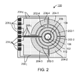
- Figure 2 schematically shows a sensor with a multitude of detectors.
- Sensor 100 shows a through-hole 112 round axis 102, the axis being perpendicular to the drawing.
- the sensor shows an annular detector 104 and an annular detector 106 surrounding detector 104.
- a number of detectors 202-i, with i 1..4, arranged around the annular detector 106, together forming an annulus.
- four detectors 204-i together form an annulus round detectors 202-i.
- Each connection pad is connected with a corresponding detector by a track 208-j.
- back-scattered electrons are detected by the detectors further removed from the axis. These detectors are segmented in four 90° segments.
- the topographical information of the sample can be determined by comparing the signal induced in corresponding segments, as well by comparing the signal from different annuli.
- backscattered electrons also have more energy than secondary electrons, and thus generate more electron-hole pairs, provided all energy of these electrons is dissipated in the active region of the detector: any electron/hole pairs generated in the n-doped substrate will recombine and are thus not detected.
- detectors can also be combined at different distances from the (radiation sensitive) surface. This can be done by e.g. direct bonding of two sensors onto each other, or by forming the detectors according to the invention on top of a substrate that already comprises so-named buried detectors.
- the detectors can form a PIN-bonding-PIN or a PIN-bonding-NIP structure.
- the buried detector can be used to detect radiation with a different penetration depth.
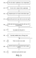
- Figure 3 schematically shows the steps for manufacturing the detector.
- step 300 an n-doped silicon substrate is provided. These substrates are readily available.
- an intrinsic layer is formed on the front-side of the substrate, for example by growing an epitaxial layer on the substrate.
- 'front-side' should be interpreted as the side of the sensor that is sensitive to radiation.
- this is a thick layer of, for example, more than 10 ⁇ m thickness.
- n-doped silicon substrates with an intrinsic layer on it are readily available, but that these do not show the thickness of, for example, more than 10 ⁇ m.
- the detector areas should preferably be defined in a surface isolation layer.
- step 302 a pure boron layer with a thickness of several nanometres is formed on the intrinsic layer.
- the pure boron layer thus forms an amorphous boron layer.
- a p + -type diffusion layer of silicon-boride is formed between the intrinsic layer and the boron layer.
- step 303 the boron layer is completely covered with a conductive material such as aluminium.
- step 304 a part of the aluminium layer covering the boron layer is removed, leaving only a thin layer of aluminium on the boron. Although most of the aluminium is removed after this step, the boron layer is not exposed to, and thus not damaged by, the dry etching. In this way the remaining aluminium protects the detector surface during (optional) back-wafer processing
- a through-hole is formed in the substrate for passing a beam of charged particles, so that the sensor can be used in e.g. a Scanning Electron Microscope (SEM).
- SEM Scanning Electron Microscope
- step 306 the inside of the through-hole is metalized to avoid charging.
- step 307 an electrode is formed on the back-side.
- step 308 the remaining aluminium layer is opened by wet etching, thereby exposing the boron layer.
- boron is more enduring to wet etching than e.g. aluminium, damage to the boron layer can be minimal.
- a protective layer for example a boron nitride or boron carbide layer, is formed on the boron layer. It is noted that a protective boron oxide layer is formed by exposing the boron layer to the atmosphere.
- the protective layer can optionally also be deposited after step 302 (deposition of the boron layer). It is further noted that, if the protective layer is sufficiently thin, its resistivity (between the boron layer and the grid) is governed by quantum effects, and that thereby the isolating properties of bulk boron compounds are of no consequence.
- step 307 By combining the dry etching of step 307 and the wet etching of step 308, the low under-etching of the dry etching is combined with the selectivity of the wet etching. The result is a process with high controllability and good pattern definition.
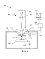
- Figure 4 schematically shows a SEM equipped with the detector.
- FIG. 4 shows a particle-optical apparatus, such as a SEM 400, equipped with a SEM column 402.
- the SEM column produces an electron beam 404.
- the SEM column is mounted on a vacuum chamber 406, the vacuum chamber comprising a sample stage 408 for holding a sample 410.
- the vacuum chamber is evacuated by vacuum pumps (not shown)
- the sample stage, or at least the sample may be biased (floated) to a potential with respect to ground by voltage source 422.
- the SEM column comprises an electron source 412, lenses 414, 416 to focus the electrons on the sample, and a deflection unit 418.
- the apparatus is further equipped with a standard SE detector, such as an Everhart-Thornley detector 420, for detecting secondary electrons, and a sensor according to the invention 100.
- the sensor 100 shows a through-hole 112 for passing the beam 404.
- the apparatus further comprises a controller 424 for controlling, amongst others, the deflection unit 418, the lenses, and the detectors 420 and 100, and displaying information gathered from the detectors on a display unit 426.
- the signals from the sensors/detectors is processed by the controller 424 and displayed.
- the processing may include combining, integrating, subtracting, false colouring, edge enhancing, and other processing known to the person skilled in the art. Also automated recognition processes, such as used for e.g. particle analysis, may be included in this processing.
- a combination of sensors/detectors may be detectors in e.g. sensor 100, but may also be a combination of signals from sensor 100 and detector 420.
- the voltage source 422 may be used to bias the sample with respect to the column. Thereby secondary electrons are accelerated towards the sensor 100 with a sufficient energy to be detected. This makes detector 420 redundant.
- germanium wafers have the benefit of generating a higher signal due to the lower band gap, resulting in more electron-hole pairs for an impinging electron with a given energy, while a GaAs wafer will show lower leakage ('dark current') at room temperature.
Landscapes
- Chemical & Material Sciences (AREA)
- Analytical Chemistry (AREA)
- Measurement Of Radiation (AREA)
- Light Receiving Elements (AREA)
- Solid State Image Pick-Up Elements (AREA)
Priority Applications (5)
| Application Number | Priority Date | Filing Date | Title |
|---|---|---|---|
| EP10150660A EP2346094A1 (fr) | 2010-01-13 | 2010-01-13 | Procédé de fabrication d'un détecteur de rayonnements |
| EP11150672A EP2346095A3 (fr) | 2010-01-13 | 2011-01-12 | Procédé de fabrication d'un détecteur de rayonnements |
| JP2011004116A JP5788182B2 (ja) | 2010-01-13 | 2011-01-12 | 放射線検出器 |
| US13/006,305 US8450820B2 (en) | 2010-01-13 | 2011-01-13 | Radiation detector |
| CN201110006527.1A CN102130218B (zh) | 2010-01-13 | 2011-01-13 | 辐射检测器 |
Applications Claiming Priority (1)
| Application Number | Priority Date | Filing Date | Title |
|---|---|---|---|
| EP10150660A EP2346094A1 (fr) | 2010-01-13 | 2010-01-13 | Procédé de fabrication d'un détecteur de rayonnements |
Publications (1)
| Publication Number | Publication Date |
|---|---|
| EP2346094A1 true EP2346094A1 (fr) | 2011-07-20 |
Family
ID=42235125
Family Applications (2)
| Application Number | Title | Priority Date | Filing Date |
|---|---|---|---|
| EP10150660A Withdrawn EP2346094A1 (fr) | 2010-01-13 | 2010-01-13 | Procédé de fabrication d'un détecteur de rayonnements |
| EP11150672A Withdrawn EP2346095A3 (fr) | 2010-01-13 | 2011-01-12 | Procédé de fabrication d'un détecteur de rayonnements |
Family Applications After (1)
| Application Number | Title | Priority Date | Filing Date |
|---|---|---|---|
| EP11150672A Withdrawn EP2346095A3 (fr) | 2010-01-13 | 2011-01-12 | Procédé de fabrication d'un détecteur de rayonnements |
Country Status (4)
| Country | Link |
|---|---|
| US (1) | US8450820B2 (fr) |
| EP (2) | EP2346094A1 (fr) |
| JP (1) | JP5788182B2 (fr) |
| CN (1) | CN102130218B (fr) |
Cited By (21)
| Publication number | Priority date | Publication date | Assignee | Title |
|---|---|---|---|---|
| EP2837031A4 (fr) * | 2012-04-10 | 2015-11-18 | Kla Tencor Corp | Capteur rétroéclairé muni d'une couche de bore |
| EP2991114A1 (fr) | 2014-08-25 | 2016-03-02 | FEI Company | Capteur de rayonnement amélioré et son application dans un microscope à faisceau de particules chargées |
| US9347890B2 (en) | 2013-12-19 | 2016-05-24 | Kla-Tencor Corporation | Low-noise sensor and an inspection system using a low-noise sensor |
| EP2880693A4 (fr) * | 2012-08-03 | 2016-06-01 | Kla Tencor Corp | Photocathode comprenant un substrat de silicium ayant une couche de bore |
| US9410901B2 (en) | 2014-03-17 | 2016-08-09 | Kla-Tencor Corporation | Image sensor, an inspection system and a method of inspecting an article |
| US9426400B2 (en) | 2012-12-10 | 2016-08-23 | Kla-Tencor Corporation | Method and apparatus for high speed acquisition of moving images using pulsed illumination |
| US9478402B2 (en) | 2013-04-01 | 2016-10-25 | Kla-Tencor Corporation | Photomultiplier tube, image sensor, and an inspection system using a PMT or image sensor |
| US9748294B2 (en) | 2014-01-10 | 2017-08-29 | Hamamatsu Photonics K.K. | Anti-reflection layer for back-illuminated sensor |
| US9767986B2 (en) | 2014-08-29 | 2017-09-19 | Kla-Tencor Corporation | Scanning electron microscope and methods of inspecting and reviewing samples |
| US9860466B2 (en) | 2015-05-14 | 2018-01-02 | Kla-Tencor Corporation | Sensor with electrically controllable aperture for inspection and metrology systems |
| US10197501B2 (en) | 2011-12-12 | 2019-02-05 | Kla-Tencor Corporation | Electron-bombarded charge-coupled device and inspection systems using EBCCD detectors |
| US10313622B2 (en) | 2016-04-06 | 2019-06-04 | Kla-Tencor Corporation | Dual-column-parallel CCD sensor and inspection systems using a sensor |
| US10462391B2 (en) | 2015-08-14 | 2019-10-29 | Kla-Tencor Corporation | Dark-field inspection using a low-noise sensor |
| US20200212246A1 (en) * | 2018-12-31 | 2020-07-02 | Asml Netherlands B.V. | Semiconductor detector and method of fabricating same |
| US10748730B2 (en) | 2015-05-21 | 2020-08-18 | Kla-Tencor Corporation | Photocathode including field emitter array on a silicon substrate with boron layer |
| US10778925B2 (en) | 2016-04-06 | 2020-09-15 | Kla-Tencor Corporation | Multiple column per channel CCD sensor architecture for inspection and metrology |
| US10943760B2 (en) | 2018-10-12 | 2021-03-09 | Kla Corporation | Electron gun and electron microscope |
| US11114491B2 (en) | 2018-12-12 | 2021-09-07 | Kla Corporation | Back-illuminated sensor and a method of manufacturing a sensor |
| US11114489B2 (en) | 2018-06-18 | 2021-09-07 | Kla-Tencor Corporation | Back-illuminated sensor and a method of manufacturing a sensor |
| US11848350B2 (en) | 2020-04-08 | 2023-12-19 | Kla Corporation | Back-illuminated sensor and a method of manufacturing a sensor using a silicon on insulator wafer |
| EP4539091A1 (fr) * | 2023-10-10 | 2025-04-16 | ASML Netherlands B.V. | Système d'imagerie à faisceau d'électrons |
Families Citing this family (33)
| Publication number | Priority date | Publication date | Assignee | Title |
|---|---|---|---|---|
| US8847480B2 (en) | 2009-03-18 | 2014-09-30 | Semiconductor Energy Laboratory Co., Ltd. | Lighting device |
| US8405116B2 (en) * | 2009-03-18 | 2013-03-26 | Semiconductor Energy Laboratory Co., Ltd. | Lighting device |
| EP2525385A1 (fr) | 2011-05-16 | 2012-11-21 | Fei Company | Microscope à particules chargées |
| EP2544025A1 (fr) | 2011-07-07 | 2013-01-09 | FEI Company | Détecteur au silicium à diffusion pour une utilisation dans un appareil de particules chargées |
| EP2557584A1 (fr) | 2011-08-10 | 2013-02-13 | Fei Company | Procédé d'imagerie par microscopie à particules chargées |
| CN103021840B (zh) * | 2011-09-23 | 2015-11-04 | 中国科学院微电子研究所 | 防止钝化层过刻蚀的方法 |
| JP5662393B2 (ja) * | 2012-08-30 | 2015-01-28 | 株式会社アドバンテスト | 電子ビーム検出器、電子ビーム処理装置及び電子ビーム検出器の製造方法 |
| NL2011568A (en) * | 2012-10-31 | 2014-05-06 | Asml Netherlands Bv | Sensor and lithographic apparatus. |
| JP6068954B2 (ja) * | 2012-11-28 | 2017-01-25 | 浜松ホトニクス株式会社 | フォトダイオードアレイ |
| CN103700719B (zh) * | 2013-12-05 | 2016-03-02 | 中国航天科技集团公司第九研究院第七七一研究所 | 一种电容式Si基辐射探测器件及其制备方法 |
| EP2924708A1 (fr) * | 2014-03-25 | 2015-09-30 | Fei Company | Imagerie d'un échantillon à l'aide de faisceaux multiples et de détecteurs multiples |
| DE102014226985B4 (de) | 2014-12-23 | 2024-02-08 | Carl Zeiss Microscopy Gmbh | Verfahren zum Analysieren eines Objekts, Computerprogrammprodukt sowie Teilchenstrahlgerät zur Durchführung des Verfahrens |
| JP6661283B2 (ja) * | 2015-05-14 | 2020-03-11 | 東京エレクトロン株式会社 | クリーニング方法及びプラズマ処理方法 |
| US9484431B1 (en) * | 2015-07-29 | 2016-11-01 | International Business Machines Corporation | Pure boron for silicide contact |
| US10126437B1 (en) * | 2017-05-15 | 2018-11-13 | Prismatic Sensors Ab | Detector for x-ray imaging |
| KR20200044100A (ko) | 2017-09-29 | 2020-04-28 | 에이에스엠엘 네델란즈 비.브이. | 하전 입자에 대한 다중 셀 검출기 |
| CN107884811A (zh) * | 2017-11-27 | 2018-04-06 | 中核控制系统工程有限公司 | 一种基于硅pin的中子探测器 |
| CN113302485A (zh) * | 2019-01-10 | 2021-08-24 | 深圳帧观德芯科技有限公司 | 基于外延层的x射线检测器及其制备方法 |
| EP3931854A1 (fr) * | 2019-02-26 | 2022-01-05 | ASML Netherlands B.V. | Détecteur de particules chargées avec élément de gain |
| EP3767663A1 (fr) * | 2019-07-16 | 2021-01-20 | FEI Company | Procédé de fabrication d'un détecteur de particules chargées |
| TWI864400B (zh) * | 2019-11-05 | 2024-12-01 | 荷蘭商Asml荷蘭公司 | 用於高速應用之大主動區域偵測器封裝 |
| EP3843141A1 (fr) * | 2019-12-23 | 2021-06-30 | Gatan, Inc. | Détecteur d'imagerie électronique comportant une couche de conduction thermique |
| CN111129226A (zh) * | 2019-12-26 | 2020-05-08 | 中国科学院微电子研究所 | 锗探测器的制造方法 |
| CN112054075B (zh) * | 2020-07-31 | 2023-01-06 | 重庆鹰谷光电股份有限公司 | 一种超高精度的硅象限光电探测器 |
| JP7404202B2 (ja) | 2020-09-14 | 2023-12-25 | 株式会社東芝 | 放射線検出器 |
| EP3971997B1 (fr) * | 2020-09-22 | 2023-07-05 | Consejo Superior de Investigaciones Científicas (CSIC) | Détecteur d'avalanche à faible gain de particules à faible pouvoir pénétrant |
| US12165835B2 (en) | 2020-12-30 | 2024-12-10 | Fei Company | Stroboscopic illumination synchronized electron detection and imaging |
| US12015046B2 (en) | 2021-02-05 | 2024-06-18 | Kla Corporation | Back-illuminated sensor with boron layer deposited using plasma atomic layer deposition |
| US11699607B2 (en) * | 2021-06-09 | 2023-07-11 | Kla Corporation | Segmented multi-channel, backside illuminated, solid state detector with a through-hole for detecting secondary and backscattered electrons |
| CN114093652B (zh) * | 2021-10-27 | 2024-05-31 | 浙江田中精机股份有限公司 | 一种套管及导线进线机构 |
| DE102022104133B4 (de) * | 2022-02-22 | 2025-07-03 | KETEK GmbH Halbleiter- und Reinraumtechnik | Strahlungsdetektor für Röntgenstrahlung und Betriebsverfahren |
| US20240243143A1 (en) * | 2023-01-12 | 2024-07-18 | Kla Corporation | Boron-Coated Back-Illuminated Image Sensor With Fluoride-Based Anti-Reflection Coating |
| US12484316B2 (en) | 2024-02-29 | 2025-11-25 | Kla Corporation | CVD boron uniformity overcoming loading effects |
Citations (7)
| Publication number | Priority date | Publication date | Assignee | Title |
|---|---|---|---|---|
| US4238760A (en) | 1978-10-06 | 1980-12-09 | Recognition Equipment Incorporated | Multi-spectrum photodiode devices |
| US5320878A (en) * | 1992-01-10 | 1994-06-14 | Martin Marietta Energy Systems, Inc. | Method of chemical vapor deposition of boron nitride using polymeric cyanoborane |
| JP2003282017A (ja) * | 2002-03-25 | 2003-10-03 | Hamamatsu Photonics Kk | 電子線検出器 |
| US20040021061A1 (en) * | 2002-07-30 | 2004-02-05 | Frederik Bijkerk | Photodiode, charged-coupled device and method for the production |
| US20050133838A1 (en) * | 2003-12-17 | 2005-06-23 | Samsung Electronics Co., Ltd. | Photodiode and method of manufacturing the same |
| US20060038176A1 (en) * | 2004-08-20 | 2006-02-23 | Kengo Akimoto | Semiconductor device and manufacturing method thereof |
| EP2009705A2 (fr) | 2007-06-25 | 2008-12-31 | ASML Netherlands B.V. | Détecteur de radiation, procédé de fabrication du détecteur de radiation et appareil lithographique comportant ce détecteur de radiation |
Family Cites Families (7)
| Publication number | Priority date | Publication date | Assignee | Title |
|---|---|---|---|---|
| JPH05258701A (ja) | 1992-03-16 | 1993-10-08 | Hitachi Ltd | 電子線装置 |
| JPH10107239A (ja) * | 1996-09-27 | 1998-04-24 | Sony Corp | 固体撮像素子およびその製造方法 |
| US6175145B1 (en) * | 1997-07-26 | 2001-01-16 | Samsung Electronics Co., Ltd. | Method of making a fuse in a semiconductor device and a semiconductor device having a fuse |
| JP3652095B2 (ja) * | 1998-01-21 | 2005-05-25 | シャープ株式会社 | 回路内蔵受光素子の製造方法 |
| WO2007146375A2 (fr) | 2006-06-14 | 2007-12-21 | Government Of The United States Of America, As Represented By The Secretary Department Of Health And Human Services | Composés de pyrimido-dione-quinoléine hautement solubles et procédés de traitement du cancer |
| EP1956633A3 (fr) | 2007-02-06 | 2009-12-16 | FEI Company | Appareil optique corpusculaire pour l'observation simultanée d'un échantillon avec des particules et des photons |
| US8138485B2 (en) | 2007-06-25 | 2012-03-20 | Asml Netherlands B.V. | Radiation detector, method of manufacturing a radiation detector, and lithographic apparatus comprising a radiation detector |
-
2010
- 2010-01-13 EP EP10150660A patent/EP2346094A1/fr not_active Withdrawn
-
2011
- 2011-01-12 JP JP2011004116A patent/JP5788182B2/ja active Active
- 2011-01-12 EP EP11150672A patent/EP2346095A3/fr not_active Withdrawn
- 2011-01-13 CN CN201110006527.1A patent/CN102130218B/zh active Active
- 2011-01-13 US US13/006,305 patent/US8450820B2/en active Active
Patent Citations (7)
| Publication number | Priority date | Publication date | Assignee | Title |
|---|---|---|---|---|
| US4238760A (en) | 1978-10-06 | 1980-12-09 | Recognition Equipment Incorporated | Multi-spectrum photodiode devices |
| US5320878A (en) * | 1992-01-10 | 1994-06-14 | Martin Marietta Energy Systems, Inc. | Method of chemical vapor deposition of boron nitride using polymeric cyanoborane |
| JP2003282017A (ja) * | 2002-03-25 | 2003-10-03 | Hamamatsu Photonics Kk | 電子線検出器 |
| US20040021061A1 (en) * | 2002-07-30 | 2004-02-05 | Frederik Bijkerk | Photodiode, charged-coupled device and method for the production |
| US20050133838A1 (en) * | 2003-12-17 | 2005-06-23 | Samsung Electronics Co., Ltd. | Photodiode and method of manufacturing the same |
| US20060038176A1 (en) * | 2004-08-20 | 2006-02-23 | Kengo Akimoto | Semiconductor device and manufacturing method thereof |
| EP2009705A2 (fr) | 2007-06-25 | 2008-12-31 | ASML Netherlands B.V. | Détecteur de radiation, procédé de fabrication du détecteur de radiation et appareil lithographique comportant ce détecteur de radiation |
Non-Patent Citations (3)
| Title |
|---|
| JUTZI M ET AL: "40-Gbit/s Ge-Si photodiodes", SILICON MONOLITHIC INTEGRATED CIRCUITS IN RF SYSTEMS, 2006. DIGEST OF PAPERS. 2006 TOPICAL MEETING ON SAN DIEGO, CA, USA 18-20 JAN., 2005, PISCATAWAY, NJ, USA,IEEE LNKD- DOI:10.1109/SMIC.2005.1587978, 18 January 2005 (2005-01-18), pages 303 - 307, XP010889720, ISBN: 978-0-7803-9472-8 * |
| NORITADA SATO ET AL: "PLASMA CVD-GROWN 10B-ENRICHED BORON FILMS FOR SI NEUTRON DETECTORS", JAPANESE JOURNAL OF APPLIED PHYSICS, JAPAN SOCIETY OF APPLIED PHYSICS, JP LNKD- DOI:10.1143/JJAP.29.2526, vol. 29, no. 11 PART 01, 1 November 1990 (1990-11-01), pages 2526 - 2530, XP000263035, ISSN: 0021-4922 * |
| SARUBBI F ET AL: "Pure boron-doped photodiodes: a solution for radiation detection in EUV lithography", ESSDERC 2008 - 38TH EUROPEAN SOLID-STATE DEVICE RESEARCH CONFERENCE 15-19 SEPT. 2008 EDINBURGH, UK, 19 September 2008 (2008-09-19), ESSDERC 2008 - 38th European Solid-State Device Research Conference IOP Publishing Bristol, UK, pages 278 - 281, XP002587902, ISBN: 978-1-4244-2363-7, DOI: 10.1109/ESSDERC.2008.4681752 * |
Cited By (48)
| Publication number | Priority date | Publication date | Assignee | Title |
|---|---|---|---|---|
| US10197501B2 (en) | 2011-12-12 | 2019-02-05 | Kla-Tencor Corporation | Electron-bombarded charge-coupled device and inspection systems using EBCCD detectors |
| EP2837031A4 (fr) * | 2012-04-10 | 2015-11-18 | Kla Tencor Corp | Capteur rétroéclairé muni d'une couche de bore |
| US10446696B2 (en) | 2012-04-10 | 2019-10-15 | Kla-Tencor Corporation | Back-illuminated sensor with boron layer |
| EP3236501A1 (fr) * | 2012-04-10 | 2017-10-25 | Kla-Tencor Corporation | Capteur rétroéclairé muni d'une couche de bore |
| US9818887B2 (en) | 2012-04-10 | 2017-11-14 | Kla-Tencor Corporation | Back-illuminated sensor with boron layer |
| US10121914B2 (en) | 2012-04-10 | 2018-11-06 | Kla-Tencor Corporation | Back-illuminated sensor with boron layer |
| US9496425B2 (en) | 2012-04-10 | 2016-11-15 | Kla-Tencor Corporation | Back-illuminated sensor with boron layer |
| US10199197B2 (en) | 2012-08-03 | 2019-02-05 | Kla-Tencor Corporation | Photocathode including silicon substrate with boron layer |
| EP2880693A4 (fr) * | 2012-08-03 | 2016-06-01 | Kla Tencor Corp | Photocathode comprenant un substrat de silicium ayant une couche de bore |
| US11081310B2 (en) | 2012-08-03 | 2021-08-03 | Kla-Tencor Corporation | Photocathode including silicon substrate with boron layer |
| US9601299B2 (en) | 2012-08-03 | 2017-03-21 | Kla-Tencor Corporation | Photocathode including silicon substrate with boron layer |
| US9426400B2 (en) | 2012-12-10 | 2016-08-23 | Kla-Tencor Corporation | Method and apparatus for high speed acquisition of moving images using pulsed illumination |
| US9620341B2 (en) | 2013-04-01 | 2017-04-11 | Kla-Tencor Corporation | Photomultiplier tube, image sensor, and an inspection system using a PMT or image sensor |
| US9478402B2 (en) | 2013-04-01 | 2016-10-25 | Kla-Tencor Corporation | Photomultiplier tube, image sensor, and an inspection system using a PMT or image sensor |
| US9347890B2 (en) | 2013-12-19 | 2016-05-24 | Kla-Tencor Corporation | Low-noise sensor and an inspection system using a low-noise sensor |
| US9748294B2 (en) | 2014-01-10 | 2017-08-29 | Hamamatsu Photonics K.K. | Anti-reflection layer for back-illuminated sensor |
| US10269842B2 (en) | 2014-01-10 | 2019-04-23 | Hamamatsu Photonics K.K. | Anti-reflection layer for back-illuminated sensor |
| US9620547B2 (en) | 2014-03-17 | 2017-04-11 | Kla-Tencor Corporation | Image sensor, an inspection system and a method of inspecting an article |
| US9410901B2 (en) | 2014-03-17 | 2016-08-09 | Kla-Tencor Corporation | Image sensor, an inspection system and a method of inspecting an article |
| EP2991112A1 (fr) * | 2014-08-25 | 2016-03-02 | Fei Company | Capteur de rayonnement amélioré et son application dans un microscope à faisceau de particules chargées |
| EP2991114A1 (fr) | 2014-08-25 | 2016-03-02 | FEI Company | Capteur de rayonnement amélioré et son application dans un microscope à faisceau de particules chargées |
| US9767986B2 (en) | 2014-08-29 | 2017-09-19 | Kla-Tencor Corporation | Scanning electron microscope and methods of inspecting and reviewing samples |
| US10466212B2 (en) | 2014-08-29 | 2019-11-05 | KLA—Tencor Corporation | Scanning electron microscope and methods of inspecting and reviewing samples |
| US9860466B2 (en) | 2015-05-14 | 2018-01-02 | Kla-Tencor Corporation | Sensor with electrically controllable aperture for inspection and metrology systems |
| US10194108B2 (en) | 2015-05-14 | 2019-01-29 | Kla-Tencor Corporation | Sensor with electrically controllable aperture for inspection and metrology systems |
| US10748730B2 (en) | 2015-05-21 | 2020-08-18 | Kla-Tencor Corporation | Photocathode including field emitter array on a silicon substrate with boron layer |
| US10462391B2 (en) | 2015-08-14 | 2019-10-29 | Kla-Tencor Corporation | Dark-field inspection using a low-noise sensor |
| US10313622B2 (en) | 2016-04-06 | 2019-06-04 | Kla-Tencor Corporation | Dual-column-parallel CCD sensor and inspection systems using a sensor |
| US10764527B2 (en) | 2016-04-06 | 2020-09-01 | Kla-Tencor Corporation | Dual-column-parallel CCD sensor and inspection systems using a sensor |
| US10778925B2 (en) | 2016-04-06 | 2020-09-15 | Kla-Tencor Corporation | Multiple column per channel CCD sensor architecture for inspection and metrology |
| US11114489B2 (en) | 2018-06-18 | 2021-09-07 | Kla-Tencor Corporation | Back-illuminated sensor and a method of manufacturing a sensor |
| US10943760B2 (en) | 2018-10-12 | 2021-03-09 | Kla Corporation | Electron gun and electron microscope |
| US11114491B2 (en) | 2018-12-12 | 2021-09-07 | Kla Corporation | Back-illuminated sensor and a method of manufacturing a sensor |
| TWI820274B (zh) * | 2018-12-31 | 2023-11-01 | 荷蘭商Asml荷蘭公司 | 半導體偵測器 |
| TWI859820B (zh) * | 2018-12-31 | 2024-10-21 | 荷蘭商Asml荷蘭公司 | 在半導體偵測器中形成頂部電極之內埋部分之方法 |
| KR20210092818A (ko) * | 2018-12-31 | 2021-07-26 | 에이에스엠엘 네델란즈 비.브이. | 반도체 검출기 및 그 제조 방법 |
| US20200212246A1 (en) * | 2018-12-31 | 2020-07-02 | Asml Netherlands B.V. | Semiconductor detector and method of fabricating same |
| WO2020141042A1 (fr) * | 2018-12-31 | 2020-07-09 | Asml Netherlands B.V. | Détecteur à semi-conducteur et son procédé de fabrication |
| TWI820862B (zh) * | 2018-12-31 | 2023-11-01 | 荷蘭商Asml荷蘭公司 | 半導體偵測器 |
| US11843069B2 (en) | 2018-12-31 | 2023-12-12 | Asml Netherlands B.V. | Semiconductor detector and method of fabricating same |
| TWI910841B (zh) * | 2018-12-31 | 2026-01-01 | 荷蘭商Asml荷蘭公司 | 在半導體偵測器中形成頂部電極之內埋部分之方法 |
| KR20240008377A (ko) * | 2018-12-31 | 2024-01-18 | 에이에스엠엘 네델란즈 비.브이. | 반도체 검출기 및 그 제조 방법 |
| CN113228223B (zh) * | 2018-12-31 | 2024-10-01 | Asml荷兰有限公司 | 半导体检测器及其制造方法 |
| CN113228223A (zh) * | 2018-12-31 | 2021-08-06 | Asml荷兰有限公司 | 半导体检测器及其制造方法 |
| US12342635B2 (en) | 2018-12-31 | 2025-06-24 | Asml Netherlands B.V. | Semiconductor detector and method of fabricating same |
| US11848350B2 (en) | 2020-04-08 | 2023-12-19 | Kla Corporation | Back-illuminated sensor and a method of manufacturing a sensor using a silicon on insulator wafer |
| WO2025078213A1 (fr) * | 2023-10-10 | 2025-04-17 | Asml Netherlands B.V. | Système d'imagerie à faisceau d'électrons |
| EP4539091A1 (fr) * | 2023-10-10 | 2025-04-16 | ASML Netherlands B.V. | Système d'imagerie à faisceau d'électrons |
Also Published As
| Publication number | Publication date |
|---|---|
| EP2346095A3 (fr) | 2011-07-27 |
| JP2011145292A (ja) | 2011-07-28 |
| JP5788182B2 (ja) | 2015-09-30 |
| EP2346095A2 (fr) | 2011-07-20 |
| US20110169116A1 (en) | 2011-07-14 |
| CN102130218B (zh) | 2016-03-16 |
| US8450820B2 (en) | 2013-05-28 |
| CN102130218A (zh) | 2011-07-20 |
Similar Documents
| Publication | Publication Date | Title |
|---|---|---|
| US8450820B2 (en) | Radiation detector | |
| JP5102580B2 (ja) | 荷電粒子線応用装置 | |
| KR102390303B1 (ko) | 전자 소스 | |
| Sakic et al. | High-efficiency silicon photodiode detector for sub-keV electron microscopy | |
| CN113228223B (zh) | 半导体检测器及其制造方法 | |
| KR102862116B1 (ko) | 전자총 및 전자 현미경 | |
| JP2016046529A (ja) | 改良された放射線センサ及び当該改良された放射線センサの荷電粒子顕微鏡内での応用 | |
| JP6576257B2 (ja) | 荷電粒子検出器、及び荷電粒子線装置 | |
| EP4053245B1 (fr) | Scintillateur, appareil de mesure, spectromètre de masse et microscope électronique | |
| TW202338898A (zh) | 電子槍及電子顯微鏡 | |
| TW202249053A (zh) | 用於偵測二次及背向散射之電子的具有通孔之分段多通道背面照明固態偵測器 | |
| US12484316B2 (en) | CVD boron uniformity overcoming loading effects | |
| JP2001305234A (ja) | 半導体電子線検出器 | |
| EP4390464A1 (fr) | Détecteur pour la détection de rayonnement | |
| TW202616327A (zh) | 在半導體偵測器中形成頂部電極之內埋部分之方法 |
Legal Events
| Date | Code | Title | Description |
|---|---|---|---|
| PUAI | Public reference made under article 153(3) epc to a published international application that has entered the european phase |
Free format text: ORIGINAL CODE: 0009012 |
|
| AK | Designated contracting states |
Kind code of ref document: A1 Designated state(s): AT BE BG CH CY CZ DE DK EE ES FI FR GB GR HR HU IE IS IT LI LT LU LV MC MK MT NL NO PL PT RO SE SI SK SM TR |
|
| AX | Request for extension of the european patent |
Extension state: AL BA RS |
|
| STAA | Information on the status of an ep patent application or granted ep patent |
Free format text: STATUS: THE APPLICATION IS DEEMED TO BE WITHDRAWN |
|
| 18D | Application deemed to be withdrawn |
Effective date: 20120121 |