EP2557584A1 - Procédé d'imagerie par microscopie à particules chargées - Google Patents
Procédé d'imagerie par microscopie à particules chargées Download PDFInfo
- Publication number
- EP2557584A1 EP2557584A1 EP11177091A EP11177091A EP2557584A1 EP 2557584 A1 EP2557584 A1 EP 2557584A1 EP 11177091 A EP11177091 A EP 11177091A EP 11177091 A EP11177091 A EP 11177091A EP 2557584 A1 EP2557584 A1 EP 2557584A1
- Authority
- EP
- European Patent Office
- Prior art keywords
- sample
- value
- values
- group
- measurement
- Prior art date
- Legal status (The legal status is an assumption and is not a legal conclusion. Google has not performed a legal analysis and makes no representation as to the accuracy of the status listed.)
- Withdrawn
Links
- 239000002245 particle Substances 0.000 title claims abstract description 20
- 238000003384 imaging method Methods 0.000 title claims abstract description 14
- 238000000386 microscopy Methods 0.000 title claims abstract description 6
- 238000000034 method Methods 0.000 claims abstract description 84
- 238000005259 measurement Methods 0.000 claims abstract description 32
- 230000005855 radiation Effects 0.000 claims abstract description 29
- 230000008569 process Effects 0.000 claims abstract description 8
- 230000000704 physical effect Effects 0.000 claims abstract description 7
- 230000001678 irradiating effect Effects 0.000 claims abstract description 5
- 239000000463 material Substances 0.000 claims description 10
- 238000005530 etching Methods 0.000 claims description 6
- 238000010884 ion-beam technique Methods 0.000 claims description 6
- 238000013213 extrapolation Methods 0.000 claims description 4
- 238000000342 Monte Carlo simulation Methods 0.000 claims description 3
- 238000004458 analytical method Methods 0.000 claims description 3
- 238000005094 computer simulation Methods 0.000 claims description 3
- 238000010186 staining Methods 0.000 claims description 3
- 238000003486 chemical etching Methods 0.000 claims description 2
- 238000002679 ablation Methods 0.000 claims 1
- 238000000992 sputter etching Methods 0.000 claims 1
- 239000000523 sample Substances 0.000 description 77
- 238000013459 approach Methods 0.000 description 19
- 230000003993 interaction Effects 0.000 description 9
- 238000010894 electron beam technology Methods 0.000 description 8
- 238000012545 processing Methods 0.000 description 8
- 238000004627 transmission electron microscopy Methods 0.000 description 8
- 238000004422 calculation algorithm Methods 0.000 description 7
- 238000005457 optimization Methods 0.000 description 6
- 230000035515 penetration Effects 0.000 description 6
- 239000000203 mixture Substances 0.000 description 5
- 230000008859 change Effects 0.000 description 4
- 235000012431 wafers Nutrition 0.000 description 4
- XUIMIQQOPSSXEZ-UHFFFAOYSA-N Silicon Chemical compound [Si] XUIMIQQOPSSXEZ-UHFFFAOYSA-N 0.000 description 3
- 239000012472 biological sample Substances 0.000 description 3
- 230000001186 cumulative effect Effects 0.000 description 3
- 230000000694 effects Effects 0.000 description 3
- 230000001965 increasing effect Effects 0.000 description 3
- 239000004065 semiconductor Substances 0.000 description 3
- 229910052710 silicon Inorganic materials 0.000 description 3
- 239000010703 silicon Substances 0.000 description 3
- 238000004088 simulation Methods 0.000 description 3
- 238000003325 tomography Methods 0.000 description 3
- 238000007476 Maximum Likelihood Methods 0.000 description 2
- 230000015572 biosynthetic process Effects 0.000 description 2
- 238000006243 chemical reaction Methods 0.000 description 2
- 238000012937 correction Methods 0.000 description 2
- 238000001514 detection method Methods 0.000 description 2
- 229910003460 diamond Inorganic materials 0.000 description 2
- 239000010432 diamond Substances 0.000 description 2
- 238000002474 experimental method Methods 0.000 description 2
- 238000011478 gradient descent method Methods 0.000 description 2
- 230000004044 response Effects 0.000 description 2
- 238000001350 scanning transmission electron microscopy Methods 0.000 description 2
- 238000012360 testing method Methods 0.000 description 2
- GYHNNYVSQQEPJS-UHFFFAOYSA-N Gallium Chemical compound [Ga] GYHNNYVSQQEPJS-UHFFFAOYSA-N 0.000 description 1
- -1 Helium ions Chemical class 0.000 description 1
- 241000961787 Josa Species 0.000 description 1
- 239000000232 Lipid Bilayer Substances 0.000 description 1
- 230000001133 acceleration Effects 0.000 description 1
- 238000013477 bayesian statistics method Methods 0.000 description 1
- 230000003542 behavioural effect Effects 0.000 description 1
- 230000005540 biological transmission Effects 0.000 description 1
- 238000004364 calculation method Methods 0.000 description 1
- 239000003795 chemical substances by application Substances 0.000 description 1
- 230000009194 climbing Effects 0.000 description 1
- 238000000576 coating method Methods 0.000 description 1
- 238000004040 coloring Methods 0.000 description 1
- 238000002939 conjugate gradient method Methods 0.000 description 1
- 239000000470 constituent Substances 0.000 description 1
- 238000005520 cutting process Methods 0.000 description 1
- 230000007547 defect Effects 0.000 description 1
- 230000001419 dependent effect Effects 0.000 description 1
- 238000013461 design Methods 0.000 description 1
- 230000001066 destructive effect Effects 0.000 description 1
- 238000009826 distribution Methods 0.000 description 1
- 230000009977 dual effect Effects 0.000 description 1
- 230000002708 enhancing effect Effects 0.000 description 1
- 230000007613 environmental effect Effects 0.000 description 1
- 238000009472 formulation Methods 0.000 description 1
- 229910052733 gallium Inorganic materials 0.000 description 1
- 229910052734 helium Inorganic materials 0.000 description 1
- 239000001307 helium Substances 0.000 description 1
- 238000010237 hybrid technique Methods 0.000 description 1
- 238000007689 inspection Methods 0.000 description 1
- 238000011835 investigation Methods 0.000 description 1
- 150000002500 ions Chemical class 0.000 description 1
- 238000003754 machining Methods 0.000 description 1
- 239000011159 matrix material Substances 0.000 description 1
- 239000012528 membrane Substances 0.000 description 1
- 238000003801 milling Methods 0.000 description 1
- 238000005498 polishing Methods 0.000 description 1
- 229920013655 poly(bisphenol-A sulfone) Polymers 0.000 description 1
- 229920000642 polymer Polymers 0.000 description 1
- 239000002243 precursor Substances 0.000 description 1
- 230000002250 progressing effect Effects 0.000 description 1
- 238000000926 separation method Methods 0.000 description 1
- 238000007493 shaping process Methods 0.000 description 1
- 238000002922 simulated annealing Methods 0.000 description 1
- 238000012800 visualization Methods 0.000 description 1
- 238000009333 weeding Methods 0.000 description 1
Images


Classifications
-
- H—ELECTRICITY
- H01—ELECTRIC ELEMENTS
- H01J—ELECTRIC DISCHARGE TUBES OR DISCHARGE LAMPS
- H01J37/00—Discharge tubes with provision for introducing objects or material to be exposed to the discharge, e.g. for the purpose of examination or processing thereof
- H01J37/02—Details
- H01J37/22—Optical, image processing or photographic arrangements associated with the tube
- H01J37/222—Image processing arrangements associated with the tube
-
- G—PHYSICS
- G01—MEASURING; TESTING
- G01N—INVESTIGATING OR ANALYSING MATERIALS BY DETERMINING THEIR CHEMICAL OR PHYSICAL PROPERTIES
- G01N23/00—Investigating or analysing materials by the use of wave or particle radiation, e.g. X-rays or neutrons, not covered by groups G01N3/00 – G01N17/00, G01N21/00 or G01N22/00
- G01N23/22—Investigating or analysing materials by the use of wave or particle radiation, e.g. X-rays or neutrons, not covered by groups G01N3/00 – G01N17/00, G01N21/00 or G01N22/00 by measuring secondary emission from the material
-
- H—ELECTRICITY
- H01—ELECTRIC ELEMENTS
- H01J—ELECTRIC DISCHARGE TUBES OR DISCHARGE LAMPS
- H01J37/00—Discharge tubes with provision for introducing objects or material to be exposed to the discharge, e.g. for the purpose of examination or processing thereof
- H01J37/26—Electron or ion microscopes; Electron or ion diffraction tubes
- H01J37/28—Electron or ion microscopes; Electron or ion diffraction tubes with scanning beams
-
- G—PHYSICS
- G01—MEASURING; TESTING
- G01N—INVESTIGATING OR ANALYSING MATERIALS BY DETERMINING THEIR CHEMICAL OR PHYSICAL PROPERTIES
- G01N2223/00—Investigating materials by wave or particle radiation
- G01N2223/40—Imaging
- G01N2223/423—Imaging multispectral imaging-multiple energy imaging
-
- H—ELECTRICITY
- H01—ELECTRIC ELEMENTS
- H01J—ELECTRIC DISCHARGE TUBES OR DISCHARGE LAMPS
- H01J2237/00—Discharge tubes exposing object to beam, e.g. for analysis treatment, etching, imaging
- H01J2237/22—Treatment of data
- H01J2237/226—Image reconstruction
Definitions
- the invention relates to a method of investigating a sample using charged-particle microscopy, comprising the following steps:
- the invention also relates to an apparatus for performing such a method.
- a method as set forth in the opening paragraph is known from United States Patent US 5,412,210 , and makes use of the insight that changing the primary beam energy in a Scanning Electron Microscope (SEM) leads to deeper penetration inside the sample being investigated.
- SEM Scanning Electron Microscope
- such an approach can be used to generate quasi-tomograms of regions of interest in the sample.
- attempts to exploit this approach have involved acquiring two or more images with increasing primary beam energy, adjusting contrast between the images, and then subtracting lower-energy images from higher-energy images to reveal submerged layers in the sample.
- a method as set forth in the opening paragraph is also known from co-pending European patent application EP-A 11163992 (FNL1015), which shares a common inventor with the current invention.
- a sample is probed by a SEM electron beam at a range of different beam parameters, and the intensity of backscattered (BS) electrons emanating from the sample is measured.
- the data thus obtained are subsequently automatically processed, by using second-order and higher-order statistics from a range of Blind Source Separation techniques to deconvolute signals coming from different layer depths (z-levels) within the sample. In this way, one is able to calculate a set of images of the sample for a corresponding set of said different layer depths.
- a drawback of the approach in the previous paragraph is that it assumes that the region of interaction of the probing electron beam with the sample is basically only longitudinal in form (i.e. essentially one-dimensional, along a z-axis), with essentially no lateral spread (i.e. no higher-dimensional components, along x/y axes).
- a simplification can correlate relatively closely to reality in certain situations, e.g. when using a probing electron beam with relatively low landing energies, it can deviate more significantly from reality in other situations, e.g.
- the invention exploits a number of insights that allowed the above-mentioned mathematical approach to be developed.
- the inventor realized that:
- said constraints on the values K n are derived using at least one method selected from the group comprising:
- said minimum divergence is selected from the group comprising Least Squares Distance, Csiszar-Morimoto F-divergences, Bregman Divergences, Alpha-Beta-Divergences, the Bhattacharyya Distance, the Cramér-Rao Bound, derivatives of these, and combinations hereof.
- the particular choice of the type of divergence will depend inter alia on the statistical nature of the assumed noise in the computation in question.
- the actual minimization (i.e. optimization) of the chosen divergence can be performed using a variety of techniques, such as Gradient-Descent methods, Stochastic methods, and Expectation-Maximization Maximum Likelihood and Maximum ⁇ Priori methods, for example. Iterative techniques which use derivatives, among which the Gradient Descent method, Conjugate Gradient method, Newton's method, the Quasi-Newton method, the Levenberg-Marquardt method, and Interior Point methods are some of the most commonly used; the convergence of such methods can be ensured by employing Line-Searches and Trust-Region methods, for example. As an alternative to gradient-based iterative techniques, one can employ optimization heuristics that impose fewer or no constraints on the functions to be optimized.
- Such heuristic methods search for solutions by relying mostly on stochastic strategies. Examples include Simulated Annealing, Evolutionary Algorithms, the Tabu Search, and Particle Swarm Optimization. Other popular heuristics include the Nelder-Mead Simplex and Hill Climbing algorithms, for example. For more information on such minimization techniques, see reference [4] quoted in Embodiment 2 below, and also refer to the following sources:
- computational slicing involves the physical removal of (at least one layer of) material from the sample, and may, for example, be performed using mechanical techniques (e.g. using a microtome / diamond knife) and/or radiative/ablative techniques (e.g.
- the employed layer removal procedure need not be destructive: instead, there are (mechanical) techniques that allow a removed layer to be preserved and (re-)imaged at a later juncture, if desired.
- the multi-dimensional deconvolution technique allows full 3D deconvolution of accrued data.
- the invention may, for example, also be used to perform two-dimensional (2D) or quasi-three-dimensional (so-called 2.5D) deconvolution.
- 2D two-dimensional
- 2.5D quasi-three-dimensional
- Figure 1 schematically depicts part of a measurement sequence comprised in an embodiment of a method according to the current invention.
- the figure has three sub-figures, (A)-(C), respectively representing three successive measurement sessions in said sequence [1,...,N].
- a general member of the sequence [1,...,N] is denoted by the integer n.
- Each sub-figure renders a cross-sectional view of an interaction between an incoming probing beam of radiation 1 and a portion of a sample 3 being investigated.
- the beam 1 propagates in a z direction but, when it strikes the sample 3, it produces a multi-dimensional interaction region 5 within the sample 3, with a longitudinal component in z and with lateral components in x and y.
- a parameter P of the beam 1 has had its value changed between measurement sessions, e.g. having distinct values P 1 , P 2 and P 3 for the three sub-figures, respectively.
- This parameter P may, for example, be the landing energy of the beam 1.
- PSF kernel values K 1 , K 2 and K 3 are associated with the beam parameter values P 1 , P 2 and P 3 , respectively.
- the interaction of the beam 1 with the sample 3 produces stimulated radiation 7, which originates from the interaction region 5 and is generally emitted from the surface of the sample 3 facing the incoming beam 1.
- this stimulated radiation 7 is denoted using a single arrow, so as not to clutter the figure; however, in reality, such stimulated radiation 7 will be emitted in a whole range of directions. Examples of such stimulated radiation are BS electrons, secondary electrons and X-rays.
- the stimulated radiation 7 can be detected.
- a measurand M e.g. detector current or intensity
- measurand values M 1 , M 2 and M 3 are obtained, corresponding to the PSF kernel values K 1 , K 2 and K 3 , respectively.
- the sample 3 has a physical property O that influences the sample's interaction with the incoming beam 1; for example, O might be the atomic density or secondary emission coefficient of the sample.
- O might be the atomic density or secondary emission coefficient of the sample.
- This functional form is represented here by a spatial variable V. Distilling information about V will generally yield important insights into the internal structure and nature of the sample 3.
- the current invention addresses this problem, by providing a computational technique by which said information can be deconvoluted (i.e. "disentangled” or spatially resolved).
- Q n K n * V.
- min D M n ⁇ K n * V min D M n ⁇ K n * V .
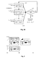
- FIG. 2B this figure represents a generalization of Figure 2A . Instead of just showing the procedure for only one element n of the measurement sequence [1,...,N], it now depicts all the elements 1...N in this sequence:
- variable-kernel deconvolution task at hand is to formulate it using so-called Bayesian statistics.
- the current imaging process is well represented by a Poisson process.
- I n ⁇ n ⁇ ⁇ ⁇ K n * V ⁇ x I n x ⁇ exp - K n * V ⁇ x I n x , wherein it should be noted that "x" is not the linear Cartesian coordinate x, but is instead an algebraic denotation of a three-dimensional position.
- IDIVI n ⁇ V J V
- the second term in (8) is a constant with regard to minimization and, hence, minimizing J((V
- the iterative algorithm needs to be sequentially used for all kernels K x associated with the different PSFs. Convergence can be assessed empirically or based on other criteria, such as the relative change in the variables.
- V ⁇ argmax V ⁇ 0 Pr V , K n
- I n - log Pr I n
- V , K n - log Pr V - log Pr K n J I n
- the second and third terms are known as regularization terms that use one's knowledge and assumptions about the variables to limit the space of solutions and reduce the effects of noise.
- I x ) can be minimized using the Maximum Likelihood Expectation Maximization approach. Optimization can be also carried using a variety of other convex and non-convex methods, as set forth, for example, in the following reference:
- RLA Richardson-Lucey Algorithm
- Figure 3 illustrates an embodiment of the current invention whereby computational slicing is combined with physical slicing, so as to allow charged-particle-microscopy-based 3D volume imaging of a sample.
- Figure 3A depicts a computational slicing step, whereby a sample is scanned at varying landing energies (E 1 , E 2 , E 3 ) and a 3D deconvolution algorithm is applied, as set forth above. This allows sub-surface virtual imaging of the sample to increasing penetration depths, here schematically labeled as (L 1 , L 2 , L 3 ).
- Figure 3B subsequent use is made of a physical slicing step, whereby a mechanical cutting device (e.g. a diamond knife) or a non-mechanical approach (e.g. involving a focused/broad beam of ions, or a focused electromagnetic beam) is used to physically "skim off" a certain depth of material from the sample, thus producing a newly exposed surface.
- a mechanical cutting device e.g. a diamond knife
- a non-mechanical approach e.g. involving a focused/broad beam of ions, or a focused electromagnetic beam
- Step 301 is preceded by preparatory considerations in which it is decided inter alia what energies will be used in the acquisition step.
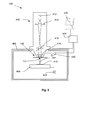
- FIG. 5 shows a charged-particle microscope 400, which, in this case, is a SEM.
- the microscope 400 comprises a particle-optical column 402, which produces a charged-particle beam 404 (in this case, an electron beam).
- the particle-optical column 402 is mounted on a vacuum chamber 406, which comprising a sample holder / stage 408 for holding a sample 410.
- the vacuum chamber 406 is evacuated using vacuum pumps (not depicted). With the aid of voltage source 422, the sample holder 408, or at least the sample 410, may be biased (floated) to an electrical potential with respect to ground.
- the particle-optical column 402 comprises an electron source 412, lenses 414, 416 to focus the electron beam 404 onto the sample 410, and a deflection unit 418.
- the apparatus is equipped with:
- stimulated radiation - comprising, for example, X-rays, secondary electrons (SEs) and backscattered electrons (BEs) - emanates from the sample 410.
- X-rays are detected by first detector 420, whereas SEs/BEs are detected by second detector 100.
- SEs/BEs are detected by second detector 100.
- the emitted radiation is position-sensitive (due to said scanning motion), the information obtained from the detectors 420, 100, will also be position-dependent.
- the signals from the detectors 420,100 are processed by the processing apparatus 424, and displayed on display unit 426.
- processing may include operations such as combining, integrating, subtracting, false colouring, edge enhancing, and other processing known to the person skilled in the art.
- automated recognition processes e.g. as used for particle analysis, may be included in such processing.
Landscapes
- Chemical & Material Sciences (AREA)
- Analytical Chemistry (AREA)
- Engineering & Computer Science (AREA)
- Computer Vision & Pattern Recognition (AREA)
- Physics & Mathematics (AREA)
- Health & Medical Sciences (AREA)
- Life Sciences & Earth Sciences (AREA)
- Biochemistry (AREA)
- General Health & Medical Sciences (AREA)
- General Physics & Mathematics (AREA)
- Immunology (AREA)
- Pathology (AREA)
- Analysing Materials By The Use Of Radiation (AREA)
Priority Applications (13)
| Application Number | Priority Date | Filing Date | Title |
|---|---|---|---|
| EP11177091A EP2557584A1 (fr) | 2011-08-10 | 2011-08-10 | Procédé d'imagerie par microscopie à particules chargées |
| EP12163262A EP2557585A1 (fr) | 2011-08-10 | 2012-04-05 | Microscope à particules chargées fournissant une imagerie à résolution en profondeur |
| EP12179764.1A EP2557587B1 (fr) | 2011-08-10 | 2012-08-09 | Microscope à particules chargées fournissant une imagerie à résolution en profondeur |
| JP2012176833A JP6099900B2 (ja) | 2011-08-10 | 2012-08-09 | 荷電粒子顕微鏡による可視化法 |
| JP2012176834A JP6195699B2 (ja) | 2011-08-10 | 2012-08-09 | 検査方法及び荷電粒子顕微鏡 |
| EP12179763.3A EP2557586B1 (fr) | 2011-08-10 | 2012-08-09 | Procédé d'imagerie par microscopie à particules chargées |
| CN201210283730.8A CN102931044B (zh) | 2011-08-10 | 2012-08-10 | 提供深度分辨图像的带电粒子显微镜 |
| US13/572,449 US8586921B2 (en) | 2011-08-10 | 2012-08-10 | Charged-particle microscope providing depth-resolved imagery |
| US13/572,206 US8581189B2 (en) | 2011-08-10 | 2012-08-10 | Charged particle microscopy imaging method |
| CN201210283575.XA CN102954773B (zh) | 2011-08-10 | 2012-08-10 | 带电粒子显微成像方法 |
| EP13153164.2A EP2648207A1 (fr) | 2011-08-10 | 2013-01-30 | Microscope à particules chargées fournissant une imagerie à résolution en profondeur |
| US13/856,899 US8704176B2 (en) | 2011-08-10 | 2013-04-04 | Charged particle microscope providing depth-resolved imagery |
| US14/257,742 US9711325B2 (en) | 2011-08-10 | 2014-04-21 | Charged-particle microscope providing depth-resolved imagery |
Applications Claiming Priority (1)
| Application Number | Priority Date | Filing Date | Title |
|---|---|---|---|
| EP11177091A EP2557584A1 (fr) | 2011-08-10 | 2011-08-10 | Procédé d'imagerie par microscopie à particules chargées |
Publications (1)
| Publication Number | Publication Date |
|---|---|
| EP2557584A1 true EP2557584A1 (fr) | 2013-02-13 |
Family
ID=45894711
Family Applications (5)
| Application Number | Title | Priority Date | Filing Date |
|---|---|---|---|
| EP11177091A Withdrawn EP2557584A1 (fr) | 2011-08-10 | 2011-08-10 | Procédé d'imagerie par microscopie à particules chargées |
| EP12163262A Withdrawn EP2557585A1 (fr) | 2011-08-10 | 2012-04-05 | Microscope à particules chargées fournissant une imagerie à résolution en profondeur |
| EP12179763.3A Active EP2557586B1 (fr) | 2011-08-10 | 2012-08-09 | Procédé d'imagerie par microscopie à particules chargées |
| EP12179764.1A Active EP2557587B1 (fr) | 2011-08-10 | 2012-08-09 | Microscope à particules chargées fournissant une imagerie à résolution en profondeur |
| EP13153164.2A Withdrawn EP2648207A1 (fr) | 2011-08-10 | 2013-01-30 | Microscope à particules chargées fournissant une imagerie à résolution en profondeur |
Family Applications After (4)
| Application Number | Title | Priority Date | Filing Date |
|---|---|---|---|
| EP12163262A Withdrawn EP2557585A1 (fr) | 2011-08-10 | 2012-04-05 | Microscope à particules chargées fournissant une imagerie à résolution en profondeur |
| EP12179763.3A Active EP2557586B1 (fr) | 2011-08-10 | 2012-08-09 | Procédé d'imagerie par microscopie à particules chargées |
| EP12179764.1A Active EP2557587B1 (fr) | 2011-08-10 | 2012-08-09 | Microscope à particules chargées fournissant une imagerie à résolution en profondeur |
| EP13153164.2A Withdrawn EP2648207A1 (fr) | 2011-08-10 | 2013-01-30 | Microscope à particules chargées fournissant une imagerie à résolution en profondeur |
Country Status (4)
| Country | Link |
|---|---|
| US (2) | US8581189B2 (fr) |
| EP (5) | EP2557584A1 (fr) |
| JP (2) | JP6099900B2 (fr) |
| CN (2) | CN102954773B (fr) |
Cited By (1)
| Publication number | Priority date | Publication date | Assignee | Title |
|---|---|---|---|---|
| WO2023151946A1 (fr) | 2022-02-10 | 2023-08-17 | Carl Zeiss Smt Gmbh | Procédé d'étude couche par couche d'un échantillon semi-conducteur et dispositif d'étude pour mettre en œuvre un tel procédé |
Families Citing this family (44)
| Publication number | Priority date | Publication date | Assignee | Title |
|---|---|---|---|---|
| US8476585B2 (en) * | 2011-03-02 | 2013-07-02 | Gatan, Inc. | Microtome utilizing a movable knife in a retardation field scanning electron microscope and a retardation field scanning electron microscope including the same |
| EP2605005A1 (fr) * | 2011-12-14 | 2013-06-19 | FEI Company | Groupage de données multimodales |
| EP2557584A1 (fr) * | 2011-08-10 | 2013-02-13 | Fei Company | Procédé d'imagerie par microscopie à particules chargées |
| US8704176B2 (en) | 2011-08-10 | 2014-04-22 | Fei Company | Charged particle microscope providing depth-resolved imagery |
| FR2979165B1 (fr) * | 2011-08-16 | 2014-05-16 | Commissariat Energie Atomique | Procede de correction des effets de proximite electronique utilisant des fonctions de diffusion decentrees |
| EP2648208B1 (fr) * | 2012-04-05 | 2017-08-09 | Fei Company | Microscope à particules chargées fournissant une imagerie à résolution en profondeur |
| EP2708874A1 (fr) | 2012-09-12 | 2014-03-19 | Fei Company | Procédé permettant de réaliser une imagerie tomographique d'un échantillon dans un microscope à faisceau de particules chargées |
| DE102012217761B4 (de) * | 2012-09-28 | 2020-02-06 | Carl Zeiss Microscopy Gmbh | Verfahren zur Vermeidung von Artefakten beim Serial Block Face Imaging |
| EP2735866A1 (fr) | 2012-11-27 | 2014-05-28 | Fei Company | Procédé de prélèvement d'un échantillon et d'affichage d'informations obtenues |
| EP2738786A1 (fr) | 2012-11-29 | 2014-06-04 | Fei Company | Procédé permettant de réaliser une imagerie tomographique d'un échantillon dans un microscope à faisceau de particules chargées |
| TWI461653B (zh) * | 2013-02-06 | 2014-11-21 | Inotera Memories Inc | 測量樣本尺寸的方法 |
| GB201302624D0 (en) * | 2013-02-14 | 2013-04-03 | Univ Antwerpen | High-resolution amplitude contrast imaging |
| US9190241B2 (en) * | 2013-03-25 | 2015-11-17 | Hermes-Microvision, Inc. | Charged particle beam apparatus |
| US9177758B2 (en) * | 2013-03-25 | 2015-11-03 | Hermes Microvision Inc. | Charged particle beam apparatus |
| JP2014216213A (ja) * | 2013-04-26 | 2014-11-17 | 株式会社日立ハイテクノロジーズ | 荷電粒子顕微鏡装置および荷電粒子顕微鏡装置の画像取得方法 |
| EP2824445B1 (fr) * | 2013-07-08 | 2016-03-02 | Fei Company | Microscopie à particules chargées combinée avec spectroscopie raman |
| EP2958130A1 (fr) | 2014-06-18 | 2015-12-23 | Fei Company | Reconstruction d'image mathématique dans un microscope de type balayage |
| EP2963672A1 (fr) | 2014-06-30 | 2016-01-06 | FEI Company | Microscopie à balayage assistée par ordinateur à résolution améliorée |
| US9627175B2 (en) * | 2014-10-17 | 2017-04-18 | Jeol Ltd. | Electron microscope and elemental mapping image generation method |
| DE102014226985B4 (de) | 2014-12-23 | 2024-02-08 | Carl Zeiss Microscopy Gmbh | Verfahren zum Analysieren eines Objekts, Computerprogrammprodukt sowie Teilchenstrahlgerät zur Durchführung des Verfahrens |
| US9842724B2 (en) * | 2015-02-03 | 2017-12-12 | Kla-Tencor Corporation | Method and system for imaging of a photomask through a pellicle |
| US10236156B2 (en) | 2015-03-25 | 2019-03-19 | Hermes Microvision Inc. | Apparatus of plural charged-particle beams |
| EP3082150B1 (fr) * | 2015-04-15 | 2017-07-19 | FEI Company | Procédé et microscope à particules chargées à balayage en transmission pour imagerie tomographique |
| US9502211B1 (en) | 2015-05-03 | 2016-11-22 | Fei Company | Adaptive scanning for particle size using directed beam signal analysis |
| US10056224B2 (en) | 2015-08-10 | 2018-08-21 | Kla-Tencor Corporation | Method and system for edge-of-wafer inspection and review |
| JP6527799B2 (ja) | 2015-09-25 | 2019-06-05 | 株式会社日立ハイテクノロジーズ | 荷電粒子線装置及びパターン測定装置 |
| EP3174085A1 (fr) | 2015-11-30 | 2017-05-31 | FEI Company | Ensemble filtre pour discrimination entre des électrons secondaires et des électrons rétrodiffusés dans un microscope à particules chargées de non-transmission |
| EP3179229B1 (fr) * | 2015-12-11 | 2019-01-30 | FEI Company | Préparation d'échantillon cryogénique pour microscopie à particules chargées |
| EP3240013B1 (fr) * | 2016-04-26 | 2018-11-07 | FEI Company | Imagerie tridimensionnelle dans la microscopie à particules chargées |
| DE102016208689B4 (de) | 2016-05-20 | 2018-07-26 | Carl Zeiss Microscopy Gmbh | Verfahren zum Erzeugen eines Bildes eines Objekts und/oder einer Darstellung von Daten über das Objekt sowie Computerprogrammprodukt und Teilchenstrahlgerät zur Durchführung des Verfahrens |
| EP3297018B1 (fr) * | 2016-09-19 | 2019-03-27 | FEI Company | Procédé d'imagerie tomographique |
| US11205103B2 (en) | 2016-12-09 | 2021-12-21 | The Research Foundation for the State University | Semisupervised autoencoder for sentiment analysis |
| US10840056B2 (en) | 2017-02-03 | 2020-11-17 | Kla Corporation | Multi-column scanning electron microscopy system |
| JP6796813B2 (ja) * | 2017-02-10 | 2020-12-09 | パナソニックIpマネジメント株式会社 | 応力測定システムおよび応力測定方法 |
| DE102017119531A1 (de) * | 2017-08-25 | 2019-02-28 | Carl Zeiss Microscopy Gmbh | Hochauflösende 2D-Mikroskopie mit verbesserter Schnittdicke |
| EP3499459A1 (fr) | 2017-12-18 | 2019-06-19 | FEI Company | Procédé, dispositif et système d'apprentissage profond à distance pour la segmentation et la reconstruction d'images microscopiques |
| DE102018007455B4 (de) * | 2018-09-21 | 2020-07-09 | Carl Zeiss Multisem Gmbh | Verfahren zum Detektorabgleich bei der Abbildung von Objekten mittels eines Mehrstrahl-Teilchenmikroskops, System sowie Computerprogrammprodukt |
| US10872746B2 (en) * | 2018-11-02 | 2020-12-22 | Decision Sciences International Corporation | System of mobile charged particle detectors and methods of spent nuclear fuel imaging |
| US20200312611A1 (en) | 2019-03-29 | 2020-10-01 | Fei Company | Artificial intelligence enabled volume reconstruction |
| EP3745442A1 (fr) * | 2019-05-29 | 2020-12-02 | FEI Company | Procédé d'examen d'un échantillon à l'aide d'un microscope à particules chargées |
| CN110162904B (zh) * | 2019-05-29 | 2023-03-10 | 哈尔滨工业大学(深圳) | 金属-介电多层柱状光学纳米天线的贝叶斯优化设计方法 |
| DE102019133658A1 (de) * | 2019-12-10 | 2021-06-10 | Carl Zeiss Smt Gmbh | Vorrichtung und Verfahren zum Bearbeiten einer mikrostrukturierten Komponente |
| US12480898B2 (en) | 2022-09-01 | 2025-11-25 | Applied Materials Israel Ltd. | Z-profiling of wafers based on X-ray measurements |
| US12456600B2 (en) | 2023-05-29 | 2025-10-28 | Applied Materials Israel Ltd. | Scanning electron microscopy-based tomography of specimens |
Citations (2)
| Publication number | Priority date | Publication date | Assignee | Title |
|---|---|---|---|---|
| US5412210A (en) | 1990-10-12 | 1995-05-02 | Hitachi, Ltd. | Scanning electron microscope and method for production of semiconductor device by using the same |
| US20110187847A1 (en) * | 2008-09-08 | 2011-08-04 | Jie Bai | Scanning type charged particle microscope device and method for processing image acquired with scanning type charged particle microscope device |
Family Cites Families (27)
| Publication number | Priority date | Publication date | Assignee | Title |
|---|---|---|---|---|
| JPS56141155A (en) * | 1980-04-04 | 1981-11-04 | Hitachi Ltd | Analyzed sample position setter |
| JPH0676975B2 (ja) * | 1984-09-26 | 1994-09-28 | 新技術事業団 | 表面原子配列構造の観察方法 |
| JPH0233845A (ja) * | 1988-07-22 | 1990-02-05 | Nec Corp | 走査型電子顕微鏡 |
| JPH08329875A (ja) * | 1995-06-01 | 1996-12-13 | Hitachi Ltd | 走査型電子顕微鏡及びその試料像表示方法 |
| DE19828476A1 (de) * | 1998-06-26 | 1999-12-30 | Leo Elektronenmikroskopie Gmbh | Teilchenstrahlgerät |
| FI105438B (fi) | 1998-09-21 | 2000-08-15 | Nokia Networks Oy | Yhteydenmuodostus langattomassa tietoliikenneverkossa |
| EP0989141A1 (fr) | 1998-09-25 | 2000-03-29 | Fina Research S.A. | Elaboration de polyéthylène multimodal |
| DE19946317C1 (de) | 1999-09-28 | 2001-03-01 | Sedra Asphalt Technik Biebrich | Verfahren zur Herstellung eines schallgedämmten Gleises |
| EP1209737B2 (fr) * | 2000-11-06 | 2014-04-30 | Hitachi, Ltd. | Méthode de fabrication d'un échantillon |
| JP2002310959A (ja) * | 2001-04-16 | 2002-10-23 | Shimadzu Corp | 電子線分析装置 |
| US20030132382A1 (en) * | 2001-12-18 | 2003-07-17 | Sogard Michael R. | System and method for inspecting a mask |
| KR101041661B1 (ko) * | 2003-07-30 | 2011-06-14 | 어플라이드 머티리얼즈 이스라엘 리미티드 | 다중 검출기들을 갖는 스캐닝 전자 현미경 및 다중 검출기기반 이미징을 위한 방법 |
| US20060043291A1 (en) * | 2004-08-26 | 2006-03-02 | Peng Gang G | Electron spectroscopic metrology system |
| US7411188B2 (en) * | 2005-07-11 | 2008-08-12 | Revera Incorporated | Method and system for non-destructive distribution profiling of an element in a film |
| NL1029847C2 (nl) * | 2005-09-01 | 2007-03-05 | Fei Co | Werkwijze voor het bepalen van lensfouten in een deeltjes-optisch apparaat. |
| JP4728186B2 (ja) * | 2006-07-20 | 2011-07-20 | シャープ株式会社 | 斜出射電子線プローブマイクロx線分析方法およびそれに用いられるプログラム、並びに、斜出射電子線プローブマイクロx線分析装置 |
| EP1890136A1 (fr) * | 2006-08-16 | 2008-02-20 | FEI Company | Procédé pour obtenir des images d'un échantillion tranché |
| JP2008177064A (ja) * | 2007-01-19 | 2008-07-31 | Hitachi High-Technologies Corp | 走査型荷電粒子顕微鏡装置および走査型荷電粒子顕微鏡装置で取得した画像の処理方法 |
| US7777185B2 (en) * | 2007-09-25 | 2010-08-17 | Ut-Battelle, Llc | Method and apparatus for a high-resolution three dimensional confocal scanning transmission electron microscope |
| CN101768008B (zh) * | 2009-01-06 | 2012-10-03 | 中国科学院金属研究所 | 结构复杂材料的三维倒易空间重构方法 |
| EP2346094A1 (fr) | 2010-01-13 | 2011-07-20 | FEI Company | Procédé de fabrication d'un détecteur de rayonnements |
| JP5764380B2 (ja) * | 2010-04-29 | 2015-08-19 | エフ イー アイ カンパニFei Company | Sem画像化法 |
| EP2461348A1 (fr) | 2010-12-06 | 2012-06-06 | FEI Company | Système de détecteur à utiliser avec une spectroscopie de microscope électronique à transmission |
| US8669524B2 (en) * | 2010-10-25 | 2014-03-11 | The Reseach Foundation of State University of New York | Scanning incremental focus microscopy |
| US9679741B2 (en) * | 2010-11-09 | 2017-06-13 | Fei Company | Environmental cell for charged particle beam system |
| EP2525385A1 (fr) | 2011-05-16 | 2012-11-21 | Fei Company | Microscope à particules chargées |
| EP2557584A1 (fr) * | 2011-08-10 | 2013-02-13 | Fei Company | Procédé d'imagerie par microscopie à particules chargées |
-
2011
- 2011-08-10 EP EP11177091A patent/EP2557584A1/fr not_active Withdrawn
-
2012
- 2012-04-05 EP EP12163262A patent/EP2557585A1/fr not_active Withdrawn
- 2012-08-09 EP EP12179763.3A patent/EP2557586B1/fr active Active
- 2012-08-09 EP EP12179764.1A patent/EP2557587B1/fr active Active
- 2012-08-09 JP JP2012176833A patent/JP6099900B2/ja active Active
- 2012-08-09 JP JP2012176834A patent/JP6195699B2/ja active Active
- 2012-08-10 US US13/572,206 patent/US8581189B2/en active Active
- 2012-08-10 CN CN201210283575.XA patent/CN102954773B/zh active Active
- 2012-08-10 US US13/572,449 patent/US8586921B2/en active Active
- 2012-08-10 CN CN201210283730.8A patent/CN102931044B/zh active Active
-
2013
- 2013-01-30 EP EP13153164.2A patent/EP2648207A1/fr not_active Withdrawn
Patent Citations (2)
| Publication number | Priority date | Publication date | Assignee | Title |
|---|---|---|---|---|
| US5412210A (en) | 1990-10-12 | 1995-05-02 | Hitachi, Ltd. | Scanning electron microscope and method for production of semiconductor device by using the same |
| US20110187847A1 (en) * | 2008-09-08 | 2011-08-04 | Jie Bai | Scanning type charged particle microscope device and method for processing image acquired with scanning type charged particle microscope device |
Non-Patent Citations (10)
| Title |
|---|
| "Chapter 12 "DUAL-BEAM (FIB-SEM) SYSTEMS" in "Introduction to Focused Ion Beams"", 1 January 2004, SPRINGER, USA, ISBN: 978-0-38-723116-7, article "Site-Specific Cross-Sectioning", pages: 250 - 255, XP055015026 * |
| ALIMOV V KH ET AL: "Depth distribution of deuterium in single- and polycrystalline tungsten up to depths of several micrometers", JOURNAL OF NUCLEAR MATERIALS, ELSEVIER BV, NL, vol. 337-339, 1 March 2005 (2005-03-01), pages 619 - 623, XP027708205, ISSN: 0022-3115, [retrieved on 20050301] * |
| CICHOCKI, A, AMARI, S: "Families of Alpha-Beta-and Gamma-Divergences: Flexible and Robust Measures of Similarities", ENTROPY, vol. 12, 2010, pages 1532 - 1568 |
| CICHOCKI, A, CRUCES, S, AMARI, S.: "Generalized Alpha-Beta Divergences and Their Application to Robust Nonnegative Matrix Factorization", ENTROPY, vol. 13, 2011, pages 134 - 170 |
| H. LANTÉRI, M. ROCHE, C. AIME: "Penalized maximum likelihood image restoration with positivity constraints: multiplicative algorithms", INVERSE PROBLEMS, vol. 18, 2002, pages 1397 - 1419 |
| L. SHEPP, Y. VARDI: "Maximum-Likelihood reconstruction for emission tomography", IEEE TRANSACTIONS ON MEDICAL IMAGING, vol. MI-5, 1982, pages 16 - 22 |
| PEZZOTTI GIUSEPPE ET AL: "Spatially resolved residual stress assessments of GaN film on sapphire substrate by cathodoluminescence piezospectroscopy", JOURNAL OF APPLIED PHYSICS, AMERICAN INSTITUTE OF PHYSICS. NEW YORK, US, vol. 104, no. 2, 21 July 2008 (2008-07-21), pages 23514 - 23514, XP012116934, ISSN: 0021-8979, DOI: 10.1063/1.2956694 * |
| RICHARDSON, WILLIAM HADLEY.: "Bayesian-Based Iterative Method of Image Restoration", JOSA, vol. 62, no. 1, 1972, pages 55 - 59, XP002513976, DOI: doi:10.1364/JOSA.62.000055 |
| WILLIAM H. PRESS, SAUL A. TEUKOLSKY, WILLIAM T. VETTERLING, BRIAN P. FLANNERY: "Numerical Recipes in C: The Art of Scientific Computing", 1992 |
| ZHU WENLIANG ET AL: "Spatially resolved crack-tip stress analysis in semiconductor by cathodoluminescence piezospectroscopy", JOURNAL OF APPLIED PHYSICS, AMERICAN INSTITUTE OF PHYSICS. NEW YORK, US, vol. 101, no. 10, 30 May 2007 (2007-05-30), pages 103531 - 103531, XP012096887, ISSN: 0021-8979 * |
Cited By (2)
| Publication number | Priority date | Publication date | Assignee | Title |
|---|---|---|---|---|
| WO2023151946A1 (fr) | 2022-02-10 | 2023-08-17 | Carl Zeiss Smt Gmbh | Procédé d'étude couche par couche d'un échantillon semi-conducteur et dispositif d'étude pour mettre en œuvre un tel procédé |
| JP2025504235A (ja) * | 2022-02-10 | 2025-02-06 | カール・ツァイス・エスエムティー・ゲーエムベーハー | 半導体試料を層ごとに検査するための方法およびそのような方法を実行するための検査装置 |
Also Published As
| Publication number | Publication date |
|---|---|
| JP6099900B2 (ja) | 2017-03-22 |
| CN102954773B (zh) | 2016-12-21 |
| CN102931044A (zh) | 2013-02-13 |
| EP2557585A1 (fr) | 2013-02-13 |
| EP2557587B1 (fr) | 2015-10-07 |
| EP2557586A2 (fr) | 2013-02-13 |
| EP2557586B1 (fr) | 2014-04-02 |
| JP2013037001A (ja) | 2013-02-21 |
| JP6195699B2 (ja) | 2017-09-13 |
| EP2557586A3 (fr) | 2013-04-10 |
| JP2013037000A (ja) | 2013-02-21 |
| EP2557587A3 (fr) | 2013-04-10 |
| US8581189B2 (en) | 2013-11-12 |
| CN102954773A (zh) | 2013-03-06 |
| EP2557587A2 (fr) | 2013-02-13 |
| US8586921B2 (en) | 2013-11-19 |
| CN102931044B (zh) | 2016-09-21 |
| US20130037715A1 (en) | 2013-02-14 |
| US20130037714A1 (en) | 2013-02-14 |
| EP2648207A1 (fr) | 2013-10-09 |
Similar Documents
| Publication | Publication Date | Title |
|---|---|---|
| EP2557586B1 (fr) | Procédé d'imagerie par microscopie à particules chargées | |
| US9711325B2 (en) | Charged-particle microscope providing depth-resolved imagery | |
| EP2963673B1 (fr) | Microscopie a balayage de calcul a resolution amelioree | |
| EP3082150B1 (fr) | Procédé et microscope à particules chargées à balayage en transmission pour imagerie tomographique | |
| US8232523B2 (en) | SEM imaging method | |
| EP2648208B1 (fr) | Microscope à particules chargées fournissant une imagerie à résolution en profondeur | |
| EP3297018B1 (fr) | Procédé d'imagerie tomographique | |
| CN103367085B (zh) | 提供深度分辨图像的带电粒子显微镜 | |
| Bosch | Boughorbel et a1. |
Legal Events
| Date | Code | Title | Description |
|---|---|---|---|
| PUAI | Public reference made under article 153(3) epc to a published international application that has entered the european phase |
Free format text: ORIGINAL CODE: 0009012 |
|
| AK | Designated contracting states |
Kind code of ref document: A1 Designated state(s): AL AT BE BG CH CY CZ DE DK EE ES FI FR GB GR HR HU IE IS IT LI LT LU LV MC MK MT NL NO PL PT RO RS SE SI SK SM TR |
|
| AX | Request for extension of the european patent |
Extension state: BA ME |
|
| STAA | Information on the status of an ep patent application or granted ep patent |
Free format text: STATUS: THE APPLICATION IS DEEMED TO BE WITHDRAWN |
|
| 18D | Application deemed to be withdrawn |
Effective date: 20130814 |