EP2348546A2 - Zusammensetzung zur Bildung einer n-leitenden Diffusionsschicht, Verfahren zur Bildung einer n-leitenden Diffusionsschicht und Verfahren zur Herstellung einer photovoltaischen Zelle - Google Patents
Zusammensetzung zur Bildung einer n-leitenden Diffusionsschicht, Verfahren zur Bildung einer n-leitenden Diffusionsschicht und Verfahren zur Herstellung einer photovoltaischen Zelle Download PDFInfo
- Publication number
- EP2348546A2 EP2348546A2 EP11151994A EP11151994A EP2348546A2 EP 2348546 A2 EP2348546 A2 EP 2348546A2 EP 11151994 A EP11151994 A EP 11151994A EP 11151994 A EP11151994 A EP 11151994A EP 2348546 A2 EP2348546 A2 EP 2348546A2
- Authority
- EP
- European Patent Office
- Prior art keywords
- type diffusion
- diffusion layer
- forming
- composition
- layer
- Prior art date
- Legal status (The legal status is an assumption and is not a legal conclusion. Google has not performed a legal analysis and makes no representation as to the accuracy of the status listed.)
- Withdrawn
Links
Images

Classifications
-
- H—ELECTRICITY
- H10—SEMICONDUCTOR DEVICES; ELECTRIC SOLID-STATE DEVICES NOT OTHERWISE PROVIDED FOR
- H10F—INORGANIC SEMICONDUCTOR DEVICES SENSITIVE TO INFRARED RADIATION, LIGHT, ELECTROMAGNETIC RADIATION OF SHORTER WAVELENGTH OR CORPUSCULAR RADIATION
- H10F77/00—Constructional details of devices covered by this subclass
- H10F77/20—Electrodes
- H10F77/206—Electrodes for devices having potential barriers
- H10F77/211—Electrodes for devices having potential barriers for photovoltaic cells
-
- H—ELECTRICITY
- H10—SEMICONDUCTOR DEVICES; ELECTRIC SOLID-STATE DEVICES NOT OTHERWISE PROVIDED FOR
- H10F—INORGANIC SEMICONDUCTOR DEVICES SENSITIVE TO INFRARED RADIATION, LIGHT, ELECTROMAGNETIC RADIATION OF SHORTER WAVELENGTH OR CORPUSCULAR RADIATION
- H10F10/00—Individual photovoltaic cells, e.g. solar cells
- H10F10/10—Individual photovoltaic cells, e.g. solar cells having potential barriers
- H10F10/14—Photovoltaic cells having only PN homojunction potential barriers
-
- H—ELECTRICITY
- H10—SEMICONDUCTOR DEVICES; ELECTRIC SOLID-STATE DEVICES NOT OTHERWISE PROVIDED FOR
- H10F—INORGANIC SEMICONDUCTOR DEVICES SENSITIVE TO INFRARED RADIATION, LIGHT, ELECTROMAGNETIC RADIATION OF SHORTER WAVELENGTH OR CORPUSCULAR RADIATION
- H10F71/00—Manufacture or treatment of devices covered by this subclass
-
- H—ELECTRICITY
- H10—SEMICONDUCTOR DEVICES; ELECTRIC SOLID-STATE DEVICES NOT OTHERWISE PROVIDED FOR
- H10F—INORGANIC SEMICONDUCTOR DEVICES SENSITIVE TO INFRARED RADIATION, LIGHT, ELECTROMAGNETIC RADIATION OF SHORTER WAVELENGTH OR CORPUSCULAR RADIATION
- H10F71/00—Manufacture or treatment of devices covered by this subclass
- H10F71/121—The active layers comprising only Group IV materials
-
- H—ELECTRICITY
- H10—SEMICONDUCTOR DEVICES; ELECTRIC SOLID-STATE DEVICES NOT OTHERWISE PROVIDED FOR
- H10F—INORGANIC SEMICONDUCTOR DEVICES SENSITIVE TO INFRARED RADIATION, LIGHT, ELECTROMAGNETIC RADIATION OF SHORTER WAVELENGTH OR CORPUSCULAR RADIATION
- H10F77/00—Constructional details of devices covered by this subclass
- H10F77/20—Electrodes
-
- H—ELECTRICITY
- H10—SEMICONDUCTOR DEVICES; ELECTRIC SOLID-STATE DEVICES NOT OTHERWISE PROVIDED FOR
- H10F—INORGANIC SEMICONDUCTOR DEVICES SENSITIVE TO INFRARED RADIATION, LIGHT, ELECTROMAGNETIC RADIATION OF SHORTER WAVELENGTH OR CORPUSCULAR RADIATION
- H10F77/00—Constructional details of devices covered by this subclass
- H10F77/30—Coatings
- H10F77/306—Coatings for devices having potential barriers
- H10F77/311—Coatings for devices having potential barriers for photovoltaic cells
-
- H—ELECTRICITY
- H10—SEMICONDUCTOR DEVICES; ELECTRIC SOLID-STATE DEVICES NOT OTHERWISE PROVIDED FOR
- H10F—INORGANIC SEMICONDUCTOR DEVICES SENSITIVE TO INFRARED RADIATION, LIGHT, ELECTROMAGNETIC RADIATION OF SHORTER WAVELENGTH OR CORPUSCULAR RADIATION
- H10F77/00—Constructional details of devices covered by this subclass
- H10F77/70—Surface textures, e.g. pyramid structures
-
- H—ELECTRICITY
- H10—SEMICONDUCTOR DEVICES; ELECTRIC SOLID-STATE DEVICES NOT OTHERWISE PROVIDED FOR
- H10P—GENERIC PROCESSES OR APPARATUS FOR THE MANUFACTURE OR TREATMENT OF DEVICES COVERED BY CLASS H10
- H10P32/00—Diffusion of dopants within, into or out of wafers, substrates or parts of devices
-
- H—ELECTRICITY
- H10—SEMICONDUCTOR DEVICES; ELECTRIC SOLID-STATE DEVICES NOT OTHERWISE PROVIDED FOR
- H10P—GENERIC PROCESSES OR APPARATUS FOR THE MANUFACTURE OR TREATMENT OF DEVICES COVERED BY CLASS H10
- H10P32/00—Diffusion of dopants within, into or out of wafers, substrates or parts of devices
- H10P32/10—Diffusion of dopants within, into or out of semiconductor bodies or layers
- H10P32/14—Diffusion of dopants within, into or out of semiconductor bodies or layers within a single semiconductor body or layer in a solid phase; between different semiconductor bodies or layers, both in a solid phase
- H10P32/1408—Diffusion of dopants within, into or out of semiconductor bodies or layers within a single semiconductor body or layer in a solid phase; between different semiconductor bodies or layers, both in a solid phase from or through or into an external applied layer, e.g. photoresist or nitride layers
- H10P32/141—Diffusion of dopants within, into or out of semiconductor bodies or layers within a single semiconductor body or layer in a solid phase; between different semiconductor bodies or layers, both in a solid phase from or through or into an external applied layer, e.g. photoresist or nitride layers the applied layer comprising oxides only
-
- H—ELECTRICITY
- H10—SEMICONDUCTOR DEVICES; ELECTRIC SOLID-STATE DEVICES NOT OTHERWISE PROVIDED FOR
- H10P—GENERIC PROCESSES OR APPARATUS FOR THE MANUFACTURE OR TREATMENT OF DEVICES COVERED BY CLASS H10
- H10P32/00—Diffusion of dopants within, into or out of wafers, substrates or parts of devices
- H10P32/10—Diffusion of dopants within, into or out of semiconductor bodies or layers
- H10P32/17—Diffusion of dopants within, into or out of semiconductor bodies or layers characterised by the semiconductor material
- H10P32/171—Diffusion of dopants within, into or out of semiconductor bodies or layers characterised by the semiconductor material being group IV material
-
- H—ELECTRICITY
- H10—SEMICONDUCTOR DEVICES; ELECTRIC SOLID-STATE DEVICES NOT OTHERWISE PROVIDED FOR
- H10P—GENERIC PROCESSES OR APPARATUS FOR THE MANUFACTURE OR TREATMENT OF DEVICES COVERED BY CLASS H10
- H10P32/00—Diffusion of dopants within, into or out of wafers, substrates or parts of devices
- H10P32/10—Diffusion of dopants within, into or out of semiconductor bodies or layers
- H10P32/19—Diffusion sources
-
- Y—GENERAL TAGGING OF NEW TECHNOLOGICAL DEVELOPMENTS; GENERAL TAGGING OF CROSS-SECTIONAL TECHNOLOGIES SPANNING OVER SEVERAL SECTIONS OF THE IPC; TECHNICAL SUBJECTS COVERED BY FORMER USPC CROSS-REFERENCE ART COLLECTIONS [XRACs] AND DIGESTS
- Y02—TECHNOLOGIES OR APPLICATIONS FOR MITIGATION OR ADAPTATION AGAINST CLIMATE CHANGE
- Y02E—REDUCTION OF GREENHOUSE GAS [GHG] EMISSIONS, RELATED TO ENERGY GENERATION, TRANSMISSION OR DISTRIBUTION
- Y02E10/00—Energy generation through renewable energy sources
- Y02E10/50—Photovoltaic [PV] energy
-
- Y—GENERAL TAGGING OF NEW TECHNOLOGICAL DEVELOPMENTS; GENERAL TAGGING OF CROSS-SECTIONAL TECHNOLOGIES SPANNING OVER SEVERAL SECTIONS OF THE IPC; TECHNICAL SUBJECTS COVERED BY FORMER USPC CROSS-REFERENCE ART COLLECTIONS [XRACs] AND DIGESTS
- Y02—TECHNOLOGIES OR APPLICATIONS FOR MITIGATION OR ADAPTATION AGAINST CLIMATE CHANGE
- Y02E—REDUCTION OF GREENHOUSE GAS [GHG] EMISSIONS, RELATED TO ENERGY GENERATION, TRANSMISSION OR DISTRIBUTION
- Y02E10/00—Energy generation through renewable energy sources
- Y02E10/50—Photovoltaic [PV] energy
- Y02E10/547—Monocrystalline silicon PV cells
-
- Y—GENERAL TAGGING OF NEW TECHNOLOGICAL DEVELOPMENTS; GENERAL TAGGING OF CROSS-SECTIONAL TECHNOLOGIES SPANNING OVER SEVERAL SECTIONS OF THE IPC; TECHNICAL SUBJECTS COVERED BY FORMER USPC CROSS-REFERENCE ART COLLECTIONS [XRACs] AND DIGESTS
- Y02—TECHNOLOGIES OR APPLICATIONS FOR MITIGATION OR ADAPTATION AGAINST CLIMATE CHANGE
- Y02P—CLIMATE CHANGE MITIGATION TECHNOLOGIES IN THE PRODUCTION OR PROCESSING OF GOODS
- Y02P70/00—Climate change mitigation technologies in the production process for final industrial or consumer products
- Y02P70/50—Manufacturing or production processes characterised by the final manufactured product
Definitions
- the present invention relates to a composition for forming an n-type diffusion layer of a photovoltaic cell, a method for forming an n-type diffusion layer, a method for producing a photovoltaic cell, a paste composition and a use of the composition. More specifically, the present invention relates to a technique which enables the formation of an n-type diffusion layer on a certain portion of silicon which is a semiconductor substrate.
- a related art fabrication process of a silicon photovoltaic cell is described hereinbelow.
- a p-type silicon substrate having a textured structure formed on a light receiving side is prepared, and subsequently subjected to a treatment at a temperature of 800 to 900°C for several tens of minutes under a mixed gas atmosphere of phosphorus oxychloride (POCl 3 ), nitrogen and oxygen, thereby uniformly forming an n-type diffusion layer.
- POCl 3 phosphorus oxychloride
- nitrogen and oxygen thereby uniformly forming an n-type diffusion layer.
- the n-type diffusion layer is formed not only on the surface, but also on the side face and the rear surface.
- the n-type diffusion layer of the rear surface needs to be convened into a p+-type diffusion layer, correspondingly an aluminum paste is assigned to the n-type diffusion layer of the rear surface to achieve conversion of the n-type diffusion layer into the p + -type diffusion layer through the diffusion of aluminum.
- a method for forming an n-type diffusion layer by applying a solution containing phosphates such as phosphorus pentoxide (P 2 O 5 ) or ammonium dihydrogen phosphate (NH 4 H 2 PO 4 ) as a donor element-containing compound (for example, Japanese Patent Application Laid-Open (JP-A) No. 2002-75894 ).
- a method is known for forming a diffusion layer by applying, onto a silicone substrate, a paste that becomes a diffusion source and that contains phosphorus as a donor element, and conducting thermal diffusion (for example, Japanese Patent No. 4073968 ).
- a donor element or donor element-containing compound vaporizes from a solution or paste, similarly to the above-stated gas-phase reaction method using a mixed gas, diffusion of phosphorus occurs at the side face and rear surface during the formation of a diffusion layer, and an n-type diffusion layer is also formed in an area other than the area to which the paste is applied.
- a first embodiment according to the present invention is a composition comprising a donor element-containing glass powder and a dispersion medium.
- a second embodiment of the present invention is a use of the composition according to any one of the first embodiment for forming an n-type diffusion layer on a semiconductor substrate.
- a third embodiment of the present invention is a method for forming an n-type diffusion layer, comprising:
- an n-type diffusion layer is formed not only on one side that requires the essential n-type diffusion layer (ordinary light-receiving side, front surface), but also on the other face (non-light receiving side, rear surface) or side face. Further, even in a method involving applying a phosphorus-containing solution or paste followed by thermal diffusion, an n-type diffusion layer is also formed on portions even in addition to the front surface, similarly to the gas-phase reaction method.
- a side face should be etched, and a rear surface should be subjected to the conversion of the n-type diffusion layer into the p-type diffusion layer.
- the conversion of the n-type diffusion layer into the p-type diffusion layer is achieved by applying, on the rear surface, a paste of aluminum which is an element of Group XIII of the periodic table, followed by sintering.
- a paste containing donor element such as a phosphorus is applied as a diffusion source, has a drawback in that it is difficult to form a diffusion layer at a selective certain region.
- the present invention has been made in view of the above problems exhibited by the background art, and it is an object of the present invention to provide a composition, which is capable of forming an n-type diffusion layer on a certain portion of a substrate, without the formation of an unnecessary n-type diffusion layer in a manufacturing process of a photovoltaic cell using a silicon substrate, and furthermore is capable of forming an n + layer or an n ++ layer on a certain portion of an n-type diffusion layer when a diffusion layer is formed at a certain portion; a use of the composition for forming an n-type diffusion layer on a semiconductor substrate, in the production of a back contact-type photovoltaic cell, and in the manufacture of a solar battery; a method for forming an n-type diffusion layer; and a method for producing a photovoltaic cell.
- the invention includes the following embodiments.
- the present invention enables the formation of an n-type diffusion layer on a certain portion of a substrate, without the formation of an n-type diffusion layer at an undesirable portion in the manufacturing process of a photovoltaic cell using a silicon substrate. Furthermore, the present invention relates to the use of the composition in the production of a back contact-type photovoltaic cell and in the manufacture of a solar battery. The suitability of the composition according to the present invention for forming an n-type diffusion layer is also reflected in this specification by referring to the composition as a "composition for forming an n-type diffusion layer".
- a composition for forming an n-type diffusion layer in accordance with the present invention will be described, and then a method for forming an n-type diffusion layer and a method for producing a photovoltaic cell, using the composition for forming an n-type diffusion layer, will be described.
- the term "process” denotes not only independent processes but also processes that cannot be clearly distinguished from other processes as long as a purpose is accomplished by the process.
- "from...to" denotes a range including each of the minimum value and the maximum value of the values described in this expression.
- composition for forming an n-type diffusion layer in accordance with the present invention contains at least a donor element-containing glass powder (hereinafter, often referred to simply as “glass powder”) and a dispersion medium, and may further contain other additives as necessary, taking into consideration coatability or the like.
- a donor element-containing glass powder hereinafter, often referred to simply as “glass powder”
- dispersion medium may further contain other additives as necessary, taking into consideration coatability or the like.
- composition for forming an n-type diffusion layer refers to a material which contains a donor element-containing glass powder and is capable of forming an n-type diffusion layer through thermal diffusion of the donor element after application of the material to a silicon substrate.
- composition including the donor element-containing glass powder for forming an n-type diffusion layer in accordance with the present invention ensures that an n-type diffusion layer is formed in a desired portion, and an unnecessary n-type diffusion layer is not formed on a rear surface or side face.
- a side etching process essential in the conventionally widely used gas-phase reaction method becomes unnecessary; consequently the process is simplified.
- a process for converting an n-type diffusion layer formed on the rear surface into a p + -type diffusion layer becomes unnecessary.
- a method of forming a p + -type diffusion layer on the rear surface and the constituent material, shape and thickness of a rear surface electrode are not limited, and the range of applicable producing methods, constituent materials and shapes is widened.
- a glass powder contained in the composition for forming an n-type diffusion layer in accordance with the present invention is melted by means of sintering to form a glass layer over an n-type diffusion layer.
- a conventional gas-phase reaction method or a conventional method of applying a phosphate-containing solution or paste also forms a glass layer over an n-type diffusion layer, and therefore the glass layer formed in the present invention can be removed by etching, similarly to the conventional method. Accordingly, even when compared with the conventional method, the composition for forming an n-type diffusion layer in accordance with the present invention generates no unnecessary products and no further additional processes.
- a donor component in the glass powder is hardly volatilized even during sintering, an n-type diffusion layer is prevented from also being formed on the rear surface or side face, rather than on the front surface alone due to the generation of volatile gases. It is assumed that the reason for this is that the donor component combines with an element in a glass powder, or is absorbed into the glass, as a result of which the donor component is hardly volatilized.
- the composition for forming an n-type diffusion layer in accordance with the present invention can form an n-type diffusion layer in a desired portion at a desired concentration, it is possible to form a selective region with a high n-type dopant concentration. Meanwhile, it is difficult to form a selective region having a high n-type dopant concentration by a conventional method such as a method using a gas-phase reaction or a method using a solution containing phosphates.
- the term "donor element” refers to an element which is capable of forming an n-type diffusion layer by doping thereof on a silicon substrate.
- the donor element elements of Group XV of the periodic table can be used.
- the donor element include P (phosphorous), Sb (antimony), Bi (bismuth) and As (arsenic). From the viewpoint of safety, convenience of vitrification or the like, P or Sb is preferable.
- Examples of the donor element-containing material which is used for introducing the donor element into the donor element-containing glass powder include P 2 O 3 , P 2 O 5 , Sb 2 O 3 , Bi 2 O 3 , and As 2 O 3 . At least one selected from P 2 O 3 , P 2 O 5 and Sb 2 O 3 is preferably used.
- the melting temperature, softening point, glass-transition point, chemical durability or the like of the glass powder can be controlled by adjusting the component ratio, if necessary.
- the glass powder preferably contains the glass component material mentioned below.
- the glass component material include SiO 2 , K 2 O, Na 2 O, Li 2 O, BaO, SrO, CaO, MgO, BeO, ZnO, PbO, CdO, V 2 O 5 , SnO, ZrO 2 , WO 3 , MoO 3 , MnO, La 2 O 3 , Nb 2 O 5 , Ta 2 O 5 , Y 2 O 3 , TiO 2 , ZrO 2 , GeO 2 , TeO 2 , and Lu 2 O 3 .
- At least one selected from SiO 2 , K 2 O, Na 2 O, Li 2 O, BaO, SrO, CaO, MgO, BeO, ZnO, PbO, CdO, V 2 O 5 , SnO, ZrO 2 , and MoO 3 is preferably used.
- At least one selected from SiO 2 , K 2 O, Na 2 O, Li 2 O, BaO, SrO, CaO, MgO, BeO, ZnO, PbO, CdO, V 2 O 5 , SnO, ZrO 2 , and MoO 3 is more preferably used.
- the donor element-containing glass powder include materials including both the donor element-containing material and the glass component material, for example, P 2 O 5 based glass which includes P 2 O 5 as the donor element such as P 2 O 5 -SiO 2 (the donor element-containing material and the glass component material are listed in this order, and are listed in the same order below)-based glass, P 2 O 5 -K 2 O-based glass, P 2 O 5 -Na 2 O-based glass, P 2 O 5 -Li 2 O-based glass, P 2 O 5 -BaO-based glass, P 2 O 5 -SrO-based glass, P 2 O 5 -CaO-based glass, P 2 O 5 -MgO-based glass, P 2 O 5 -BeO-based glass, P 2 O 5 -ZnO-based glass, P 2 O 5 -CdO-based glass, P 2 O 5 -PbO-based glass, P 2 O 5 -V 2 O 5 -based glass, P 2 O 5 -S
- the donor element-containing glass powder may include two or more donor element-containing materials such as P 2 O 5 -Sb 2 O 3 , P 2 O 5 -As 2 O 3 or the like. Although composite glass containing two components was illustrated in the above, composite glass containing three or more components, such as P 2 O 5 -SiO 2 -V 2 O 5 or P 2 O 5 -SiO 2 -CaO, may also be possible.
- the content of the glass component material in the glass powder is preferably appropriately set taking into consideration the melting temperature, the softening point, the glass-transition point, and chemical durability. Generally, the content of the glass component material is preferably from 0.1% by mass to 95% by mass, and more preferably from 0.5% by mass to 90% by mass.
- glass containing at least one selected from SiO 2 , K 2 O, Na 2 O, Li 2 O, BaO, SrO, CaO, MgO, BeO, ZnO, PbO, CdO, SnO, ZrO 2 , WO 3 , MoO 3 and MnQ, as the glass component material is preferable, from a viewpoint that a reaction product with silicon does not remaine as a residue when treated with hydrofluoric acid, therefore these glasses are preferable.
- the content of V 2 O 5 is preferably from 1% by mass to 50% by mass, and more preferably from 3% by mass to 40% by mass, from the viewpoint of lowering a melting temperature or a softening point.
- the softening point of the glass powder is preferably in the range of from 200°C to 1000°C, and more preferably from 300°C to 900°C, from the viewpoint of diffusivity during the diffusion treatment, and dripping.
- the shape of the glass powder includes a substantially spherical shape, a flat shape, a block shape, a plate shape, a scale-like shape, and the like. From the viewpoint of the coating property and uniform dispersion property, it is preferably a spherical shape, a flat shape, or a plate shape.
- the particle diameter of the glass powder is preferably 100 ⁇ m or less. When a glass powder having a particle diameter of 100 ⁇ m or less is used, a smooth coated film can be easily obtained. Further, the particle diameter of the glass powder is more preferably 50 ⁇ m or less. The lower limit of the particle diameter is not particularly limited, and preferably 0.01 ⁇ m or more.
- the particle diameter of the glass powder means the average particle diameter, and may be measured by laser diffraction particle size analyzer.
- the donor element-containing glass powder is prepared according to the following procedure.
- raw materials for example, the donor element-containing material and the glass component material
- the material for the crucible include platinum, platinum-rhodium, iridium, alumina, quartz and carbon, which are appropriately selected taking into consideration the melting temperature, atmosphere, reactivity with melted materials, and the like.
- the raw materials are heated to a temperature corresponding to the glass composition in an electric furnace, thereby preparing a solution.
- stirring is preferably applied such that the solution becomes homogenous.
- the obtained solution is allowed to flow on a zirconia substrate, a carbon substrate or the like to result in vitrification of the solution.
- the glass is pulverized into a powder.
- the pulverization can be carried out by using a known method such as using a jet mill, bead mill or ball mill.
- the content of the donor element-containing glass powder in the composition for forming an n-type diffusion layer is determined taking into consideration coatability, diffusivity of donor elements, and the like.
- the content of the glass powder in the composition for forming an n-type diffusion layer is preferably from 0.1% by mass to 95% by mass, more preferably from 1% by mass to 90% by mass, still more preferably from 1.5% by mass to 85% by mass, and furthermore preferably from 2% by mass to 80% by mass.
- the dispersion medium is a medium which disperses the glass powder in the composition. Specifically, a binder, a solvent or the like is employed as the dispersion medium.
- the binder may be appropriately selected from a polyvinyl alcohol, polyacrylamides, polyvinyl amides, polyvinyl pyrrolidone, polyethylene oxides, polysulfonic acid, acrylamide alkyl sulfonic acid, cellulose derivatives such as cellulose ethers, carboxymethylcellulose, hydroxyethylcellulose and ethylcellulose, gelatin, starch and starch derivatives, sodium alginates, xanthane, guar and guar derivatives, scleroglucan and scleroglucan derivatives, tragacanth and tragacanth derivatives, dextrin and dextrin derivatives, (meth)acrylic acid resins, (meth)acrylic acid ester resins (for example, alkyl (meth)acrylate, resins, dimethlaminoethyl (meth)acrylate resins, or the like), butadiene resins, styrene resins, and copoly
- the molecular weight of the binder is not particularly limited and is preferably appropriately adjusted taking into consideration the desired viscosity of the composition.
- the solvent examples include ketone solvents such as acetone, methylethylketone, methyl-n-propylketone, methyl-iso-propylketone, methyl-n-butylketone, methyl-iso-butylketone, methyl-n-pentylketone, methyl-n-hexylketone, diethylketone, dipropylketone, di-iso-butylketone, trimethylnonanone, cyclohexanone, cyclopentanone, methylcyclohexanone, 2,4-pentanedione, acetonylacetone, ⁇ -butyrolactone, and ⁇ -valerolactone; ether solvents such as diethyl ether, methyl ethyl ether, methyl-n-propyl ether, di-iso-propyl ether, tetrahydrofuran, methyl tetrahydrofuran, di
- n-type diffusion layer a-terpinenol, diethylene glycol mono-n-butyl ether or diethylene glycol mono-n-butyl ether acetate is preferable, and a-terpinenol or diethylene glycol mono-n-butyl ether is more preferable.
- the content of the dispersion medium in the composition for forming an n-type diffusion layer is determined taking into consideration coatability and donor concentration.
- the composition for forming an n-type diffusion layer may contain other additives.
- the other additives include metals which are readily reactive with the glass powder.
- the composition for forming an n-type diffusion layer is applied on a semiconductor substrate and heat-treated at a high temperature to form an n-type diffusion layer, during which glass is formed on the surface of the substrate. This glass is removed by dipping in acid such as hydrofluoric acid, but may be difficult to remove depending on the type of glass.
- a metal such as Ag, Mn, Cu, Fe, Zn or Si
- the glass can be easily removed after acid washing.
- at least one selected from Ag, Si, Cu, Fe, Zn and Mn is preferably used.
- At least one selected from Ag, Si and Zn is more preferably used, and Ag is still more preferably used.
- the content of the metal is preferably appropriately adjusted depending on the type of glass or the type of the metal concerned. Generally, the content of the metal is preferably from 0.01% by mass to 10% by mass, relative to the glass powder.
- FIG. 1 is a schematic cross-sectional view conceptionally showing an example of the production process of a photovoltaic cell according to the present invention.
- like numbers refer to like elements throughout the specification.
- an alkaline solution is assigned to silicon substrate which is a p-type semiconductor substrate 10, thereby removing the damaged layer, and a textured structure is obtained by etching.
- the damaged layer of the silicon surface which is caused when being sliced from an ingot, is removed by using 20% by mass of caustic soda.
- a textured structure is formed by etching with a mixture of 1% by mass of caustic soda and 10% by mass of isopropyl alcohol (in the drawing, the textured structure is omitted).
- the photovoltaic cell achieves high efficiency through the formation of a textured structure on the light-receiving side (front surface) to promote optical confinement effects.
- the composition for forming an n-type diffusion layer is applied on the surface of the p-type semiconductor substrate 10, that is, a face serving as a light-receiving side, thereby forming an n-type diffusion layer-forming composition layer 11.
- the application method for example, a printing method, a spinning method, brush application, a spray method, a doctor blade method, a roll coater method, an inkjet method or the like can be used.
- the amount of coating of the composition for forming an n-type diffusion layer is not particularly limited, but is in the range of from 0.01 to 100 g/m 2 in terms of glass powder, and preferably from 0.1 to 10 g/m 2 .
- a drying process for volatilization of the solvent contained in the composition may be required after the application thereof, if necessary.
- the drying is carried out at a temperature of 80°C to 300°C, for 1 minute to 10 minutes when using a hot plate, or for 10 minutes to 30 minutes when using a dryer or the like. Since these drying conditions are dependent on the solvent composition of the composition for forming an n-type diffusion layer, the present invention is not particularly limited to the above-stated conditions.
- a producing method of a p + -type diffusion layer (high-density electric field layer) 14 of the rear surface can employ any conventional known method without being limited to the method involving conversion of an n-type diffusion layer into a p-type diffusion layer using aluminum, and the range of choices for the producing method is then widened. Accordingly, for example, by assigning the composition 13 containing an element of Group XIII of the periodic table, such as boron (B), the high-density electric field layer 14 can be formed. As the composition 13 containing an element of Group XIII of the periodic table, such as boron (B), a composition for forming an p-type diffusion layer is included.
- the composition for forming a p-type diffusion layer is composed in the same manner as the composition for forming an n-type diffusion layer, except that the glass powder contains an acceptor element, which may be an element of Group XIII of the periodic table, for example, boron (B), aluminium (Al) or gallium (Ga) or the like, instead of the donor element.
- the acceptor element-containing glass powder preferably includes at least one selected from B 2 O 3 , Al 2 O 3 and Ga 2 O 3 .
- the method for applying the composition for forming a p-type diffusion layer to a rear side of a silicon substrate is the same as the method mentioned above for applying the composition for forming an n-type diffusion layer to a silicon substrate.
- the composition for forming a p-type diffusion applied to the rear side is subjected to thermal diffusion treatment in the same manner as when the composition for forming an n-type diffusion layer is used, thereby forming the high-density electric field layer 14 on the rear side.
- the thermal diffusion treatment of the composition for forming a p-type diffusion layer is preferably simultaneously conducted with the thermal diffusion treatment of the composition for forming an n-type diffusion layer.
- the semiconductor substrate 10, on which the n-type diffusion layer-forming composition layer 11 was formed is subjected to a thermal diffusion treatment at a temperature of 600 to 1200°C.
- This thermal diffusion treatment results in diffusion of a donor element into the semiconductor substrate, thereby forming an n-type diffusion layer 12, as shown in FIG. 1(3) .
- the thermal diffusion treatment can be carried out using a known continuous furnace, batch furnace, or the like.
- the furnace atmosphere can be appropriately adjusted with air, oxygen, nitrogen, or the like.
- the treatment time of the thermal diffusion can be appropriately selected depending on the content of a donor element contained in the composition for forming an n-type diffusion layer.
- the treatment time of the thermal diffusion may be in the range of from 1 minute to 60 minutes, and preferably from 2 minutes to 30 minutes.
- the phosphoric acid glass is removed by etching.
- the etching can be carried out by using a known method, including a method of dipping a subject in an acid, such as hydrofluoric acid, a method of dipping a subject in an alkali, such as caustic soda, or the like.
- the n-type diffusion layer-forming method of the present invention for forming an n-type diffusion layer 12 using the composition for forming an n-type diffusion layer 11 according to the present invention provides the formation of an n-type diffusion layer 12 in the desired site, without the formation of an unnecessary n-type diffusion layer on the rear surface or side face. Accordingly, a side etching process for the removal of an unnecessary n-type diffusion layer formed on the side face was essential in a method for forming an n-type diffusion layer by the conventionally widely used gas-phase reaction method, but according to the producing method of the present invention, the side etching process becomes unnecessary, and consequently the process is simplified.
- the conventional producing method requires the conversion of an unnecessary n-type diffusion layer formed on the rear surface into a p-type diffusion layer
- this conversion method employs a method involving applying a paste of aluminum, which is an element of Group XIII of the periodic table, on the n-type diffusion layer of the rear surface, followed by sintering to diffuse aluminum into the n-type diffusion layer which is thereby converted into a p-type diffusion layer. Since an amount of aluminum greater than a certain level is required to achieve sufficient conversion into a p-type diffusion layer and to form the high-density electric field layer of the p + layer in this method, it was necessary to form a thick aluminum layer.
- the producing method of a p + -type diffusion layer (high-density electric field layer) 14 of the rear surface can employ any method without being limited to the method involving conversion of an n-type diffusion layer into a p-type diffusion layer using aluminum, and choices for the producing method are then broadened.
- the composition for forming a p-type diffusion layer is composed in the same manner as the composition for forming an n-type diffusion layer, except that the glass powder contains an acceptor element instead of the donor element; the composition for forming a p-type diffusion layer is applied to a rear side of a silicon substrate (i.e., the opposite surface to the surface to which the composition for forming an n-type diffusion layer is applied); and thermal diffusion treatment is carried out; thereby forming the high-density electric field layer 14 on the rear side.
- the material used for a surface electrode 20 of the rear surface is not limited to aluminum of Group XIII of the periodic table. For example Ag (silver), Cu (copper) or the like may also be used, so the thickness of the surface electrode 20 of the rear surface can be further reduced as compared to the related art.
- an antireflective film 16 is formed over the n-type diffusion layer 12.
- the antireflective film 16 is formed by using a known technique.
- the antireflective film 16 is a silicon nitride film
- the antireflective film 16 is formed by a plasma CVD method using a mixed gas of SiH 4 and NH 3 as a raw material.
- hydrogen diffuses into crystals, and an orbit which does not contribute to bonding of silicon atoms, that is, a dangling bond binds to hydrogen, which inactivates a defect (hydrogen passivation).
- the antireflective film 16 is formed under the conditions of a mixed gas NH 3 /SiH 4 flow ratio of 0.05 to 1.0, a reaction chamber pressure of 0.1 Torr to 2 Torr, a film-forming temperature of 300°C to 550°C. and a plasma discharge frequency of 100 kHz or higher.
- a metal paste for a surface electrode is printed and applied on the antireflective film 16 of the front surface (light-receiving side) by a screen printing method, followed by drying to form a surface electrode 18.
- the metal paste for a surface electrode contains (1) metal particles and (2) glass particles as essential components, and optionally (3) a resin binder, (4) other additives, and the like.
- a rear surface electrode 20 is also formed on the high-density electric field layer 14 of the rear surface.
- the constituent maternal and forming method of the rear surface electrode 20 are not particularly limited in the present invention.
- the rear surface electrode 20 may also be formed by applying the rear surface electrode paste containing a metal such as aluminum, silver or copper, followed by drying.
- a portion of the rear surface may also be provided with a silver paste for forming a silver electrode, for connection between cells in the module process.
- electrodes are sintered to complete a photovoltaic cell,
- the sintering is carried out at a temperature in the range of 600 to 900°C for several seconds to several minutes, the front surface side undergoes melting of the antireflective film 16 which is an insulating film, due to the glass particle contained in the electrode-forming metal paste, and the silicon 10 surface is also partially melted, by which metal particles (for example, silver particles) in the paste form a contact with the silicon substrate 10, followed by solidification.
- metal particles for example, silver particles
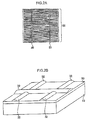
- FIG. 18 is made up of a bus bar electrode 30 and a finger electrode 32 intersecting the bus bar electrode 30.
- FIG 2A is a plan view of, as seen from the front surface, a photovoltaic cell with a configuration where the surface electrode 18 is made up of the bus bar electrode 30 and the finger electrode 32 intersecting the bus bar electrode 30, and
- FIG. 2B is a partially enlarged perspective view of FIG. 2A .
- the surface electrode 18 can be formed, for example, by the above-stated screen printing of a metal paste, or plating of electrode materials, deposition of electrode materials by electron beam heating under high vacuum, or the like. It is well known that the surface electrode 18 made up of the bus bar electrode 30 and the finger electrode 32 is typically used as an electrode for the light-receiving surface side, and a known method for the formation of the bus bar electrode and the finger electrode of the light-receiving surface side can be applied.
- the use of the composition for forming an n-type diffusion layer according to the present invention enables the production of a back-contact photovoltaic cell.
- the back-contact photovoltaic cell is intended to enlarge a light-receiving surface by providing all of the electrodes on the rear surface, That is, the back-contact photovoltaic cell is required to have a p-n junction structure by forming both an n-type diffusion region and a p + type diffusion region on the rear surface.
- the composition for forming an n-type diffusion layer according to the present invention enables the formation of an n-type diffusion portion on a certain region, and therefore can be preferably applied to the production of a back-contact photovoltaic cell,
- the particle shape of the glass powder was judged by observation with a scanning electron microscope (trade name: TM-1000, manufactured by Hitachi High-Technologies Corporation). The average diameter of the glass powder was calculated with a laser diffraction particle size analyzer (measurement wave length: 632 nm, trade name: LS 13 320, manufactured by Beckman Coulter, Inc.). The softening point of the glass powder was measured by a differential thermal analysis (DTA) curve with a Thermo Gravimetry Differential Thermal Analyzer (trade name: DTG-60H, manufactured by SHMADZU CORPORATION).
- DTA differential thermal analysis
- the prepared paste was applied to a p-type silicon substrate surface by screen printing, and dried on a hot plate at 150°C for 5 minutes to form a layer having about 18 ⁇ m thickness. Subsequently, a thermal diffusion treatment was carried out in an electric furnace at 1000°C for 10 minutes. Then, in order to remove the glass layer, the substrate was dipped in hydrofluoric acid for 5 minutes, followed by washing with running water. Some attached materials remained on the surface, but could be easily removed by rubbing with a cloth. This was followed by drying.
- the surface at the side to which the composition for forming an n-type diffusion layer was applied exhibited a sheet resistance of 186 ⁇ / ⁇ and an n-type diffusion layer was formed through diffusion of P (phosphorus) that can sufficiently function as a photovoltaic cell.
- the rear surface exhibited an unmeasurable sheet resistance of 1,000,000 ⁇ / ⁇ or higher and substantially no n-type diffusion layer was formed.
- the sheet resistance was measured by a four probe method with a low resistance meter (trade name: Loresta-EP MCP-T360, manufactured by Mitsubishi Chemical Analytech Co., Ltd.).
- An n-type diffusion layer was formed in the same manner as in Example 1, except that the thermal diffusion treatment time was 20 minutes.
- the surface at the side, where the composition for forming an n-type diffusion layer was applied exhibited a sheet resistance of 70 ⁇ / ⁇ and the formation of an n-type diffusion layer through diffusion of P (phosphorus).
- the rear surface exhibited an unmeasurable sheet resistance of 1,000,000 ⁇ / ⁇ or higher and substantially no formation of an n-type diffusion layer.
- An n-type diffusion layer was formed in the same manner as in Example 1, except that the thermal diffusion treatment time was 30 minutes.
- the surface at the side where the composition for forming an n-type diffusion layer was applied exhibited a sheet resistance of 17 ⁇ / ⁇ and the formation of an n-type diffusion layer through diffusion of P (phosphorus).
- the rear surface exhibited an unmeasurable sheet resistance of 1,000,000 ⁇ / ⁇ or higher and substantively no formation, of an n-type diffusion layer.
- An n-type diffusion layer was formed in the same manner as in Example 1. except that the glass powder was changed to P 2 O 5 -SnO-based glass whose particle shape is substantially spherical, average particle diameter is 3.2 ⁇ m and softening point is 493°C (P 2 O 5 : 70%, SnO: 20%, SiO 2 : 5%, CaO: 5%) and the furnace atmosphere when performing the thermal diffusion was nitrogen.
- the surface at the side where the composition for forming an n-type diffusion layer was applied exhibited a sheet resistance of 77 ⁇ / ⁇ and the formation of an n-type diffusion layer through diffusion of P (phosphorus).
- the rear surface exhibited an unmeasurable sheet resistance of 1,000,000 ⁇ / ⁇ or higher and substantively no formation of an n-type diffusion layer.
- An n-type diffusion layer was formed in the same manner as in Example 1, except that the glass powder was changed to P 2 O 5 -ZnO-SiO 2 -based glass powder whose particle shape is substantially spherical, average particle diameter is 2.5 ⁇ m and softening point is 460°C (P 2 OS: 60%, ZnO: 30%, SiO 2 : 10%).
- the surface at the side where the composition for forming an n-type diffusion layer was applied exhibited a sheet resistance of 10 ⁇ / ⁇ and the formation of an n-type diffusion layer through diffusion of P (phosphorus).
- the rear surface exhibited an unmeasurable sheet resistance of 1,000,000 ⁇ / ⁇ or higher and substantively no formation of an n-type diffusion layer.
- An n-type diffusion layer was formed in the same manner as in Example 1, except that the glass powder was changed to P 2 O 5 -ZnO-based glass powder whose particle shape is substantially spherical, average particle diameter is 1.3 ⁇ m and softening point is 435°C (P 2 O 5 : 65%, ZnO: 35%).
- the surface at the side where the composition for forming an n-type diffusion layer was applied exhibited a sheet resistance of 18 ⁇ / ⁇ and the formation of an n-type diffusion layer through diffusion of P. On the other hand, the rear surface exhibited an unmeasurable sheet resistance and no formation of an n-type diffusion, layer.
- An n-type diffusion layer was formed in the same manner as in Example 1, except that the glass powder was changed to P 2 O 5 -ZnO-Al 2 O 3 -based glass powder whose particle shape is substantially spherical, average particle diameter is 2.9 ⁇ m and softening point is 423°C (P 2 O 5 : 61%, ZnO: 35%, Al 2 :4%).
- the surface at the side where the composition for forming an n-type diffusion layer was applied exhibited a sheet resistance of 21 ⁇ / ⁇ and the formation of an n-type diffusion layer through diffusion of P.
- the rear surface exhibited an unmeasurable sheet resistance and substantively no formation of an n-type diffusion layer.
- An n-type diffusion layer was formed in the same manner as in Example 1, except that the glass powder was changed to P 2 O 5 -ZnO-Y 2 O 3 -based glass powder whose particle shape is substantially spherical, average particle diameter is 2.1 ⁇ m and softening point is 430°C (P 2 O 5 : 61%, ZnO: 35%, Y 2 O 3 : 4%).
- the surface at the side where the composition for forming an n-type diffusion layer was applied exhibited a sheet resistance of 25 ⁇ / ⁇ and the formation of an n-type diffusion layer through diffusion of P.
- the rear surface exhibited an unmeasurable sheet resistance and substantively no formation of an n-type diffusion layer.
- An n-type diffusion layer was formed in the same manner as in Example 1, except that the glass powder was changed to P 2 O 5 -ZnO-K 2 O-based glass powder whose particle shape is substantially spherical, average particle diameter is 2.4 ⁇ m and softening point is 395°C (P 2 O 5 : 61%, ZnO: 35%, K 2 O: 4%).
- the surface at the side where the composition for forming an n-type diffusion layer was applied exhibited a sheet resistance of 19 ⁇ / ⁇ and the formation of an n-type diffusion layer through diffusion of P.
- the rear surface exhibited an unmeasurable sheet resistance and substantively no formation of an n-type diffusion layer.
- An n-type diffusion layer was formed in the same manner as in Example 1, except that the glass powder was changed to P 2 O 5 -ZnO-K 2 O-Na 2 O-based glass powder whose particle shape is substantially spherical, average particle diameter is 3.0 ⁇ m and softening point is 406°C (P 2 O 5 : 62%, ZnO: 35%, K 2 O: 2%, Na 2 O: 1%).
- the surface at the side where the composition for forming an n-type diffusion layer was applied exhibited a sheet resistance of 21 ⁇ / ⁇ and the formation of an n-type diffusion layer through diffusion of P.
- the rear surface exhibited an unmeasurable sheet resistance and substantively no formation of an n-type diffusion layer.
- An n-type diffusion layer was formed in the same manner as in Example 1, except that the glass powder was changed to P 2 -O 5- CaO-based glass powder whose particle shape is substantially spherical, average particle diameter is 2.8 ⁇ m and softening point is 470°C (P 2 O 5 : 83%, CaO: 17%).
- the surface at the side where the composition for forming an n-type diffusion layer was applied exhibited a sheet resistance of 14 ⁇ / ⁇ and the formation of an n-type diffusion layer through diffusion of P.
- the rear surface exhibited an unmeasurable sheet resistance and substantively no formation of an n-type diffusion layer.
- An n-type diffusion layer was formed in the same manner as in Example 7, except that the composition for forming an n-type diffusion layer was applied to a half surface of a silicon substrate (5 cm ⁇ 5 cm; the same size shall apply to the following Examples) instead of the entire surface thereof, and the set temperature of the electric furnace was 950°C.
- the surface of the portion where the composition for forming an n-type diffusion layer was applied exhibited a sheet resistance of 38 ⁇ / ⁇ and the formation of an n-type diffusion layer through diffusion of P.
- the surface of the portion where the composition for forming an n-type diffusion layer was not applied exhibited an unmeasurable sheet resistance and no formation of an n-type diffusion layer, and the portion where the composition for forming an n-type diffusion layer was applied exhibited selective formation of an n-type diffusion layer. Further, the rear surface exhibited an unmeasurable sheet resistance and substantively no formation of an n-type diffusion layer.
- An n-type diffusion layer was formed in the same manner as in Example 8, except that the composition for forming an n-type diffusion layer was applied to a half surface of the silicon substrate surface instead of the entire surface thereof, and the set temperature of the electric furnace was 950°C.
- the surface of the portion where the composition for forming an n-type diffusion layer was applied exhibited a sheet resistance of 45 ⁇ / ⁇ and the formation of an n-type diffusion layer through diffusion of P.
- the surface of the portion where the composition for forming an n-type diffusion layer was not applied exhibited an unmeasurable sheet resistance and no formation of an n-type diffusion layer, and the portion where the composition for forming an n-type diffusion layer was applied exhibited selective formation of an n-type diffusion layer.
- the rear surface exhibited an unmeasurable sheet resistance and substantively no formation of an n-type diffusion layer.
- An n-type diffusion layer was formed in the same manner as in Example 9, except that the composition for forming an n-type diffusion layer was applied to a half surface of the silicon substrate surface instead of the entire surface thereof, and the set temperature of the electric furnace was 950°C.
- the surface of the portion where the composition for forming an n-type diffusion layer was applied exhibited a sheet resistance of 35 ⁇ / ⁇ and the formation of an a-type diffusion layer through diffusion of P.
- the surface of the portion where the composition for forming an n-type diffusion layer was not applied exhibited an unmeasurable sheet resistance and no formation of an n-type diffusion layer, and the portion where the composition for forming an n-type diffusion layer was applied exhibited selective formation of an n-type diffusion layer.
- the rear surface exhibited an unmeasurable sheet resistance and substantively no formation of an n-type diffusion layer.
- An n-type diffusion layer was formed in the same manner as in Example 10, except that the composition for forming an n-type diffusion layer was applied to a half surface of the silicon substrate surface instead of the entire surface thereof, and the set temperature of the electric furnace was 950°C.
- the surface of the portion where the composition for forming an n-type diffusion layer was applied exhibited a sheet resistance of 42 ⁇ / ⁇ and the formation of an n-type diffusion layer through diffusion of P.
- the surface of the portion where the composition for forming an n-type diffusion layer was not applied exhibited an unmeasurable sheet resistance and no formation of an n-type diffusion layer, and the portion where the composition for forming an n-type diffusion layer was applied exhibited selective formation of an n-type diffusion layer.
- the rear surface exhibited an unmeasurable sheet resistance and substantively no formation of an n-type diffusion layer.
- An n-type diffusion layer was formed in the same manner as in Example 11, except that the composition for forming an n-type diffusion layer was applied to a half surface of the silicon substrate surface instead of the entire surface thereof, and the set temperature of the electric furnace was 950°C.
- the surface of the portion where the composition for forming an n-type diffusion layer was applied exhibited a sheet resistance of 50 ⁇ / ⁇ and the formation of an n-type diffusion layer through diffusion of P.
- the surface of the portion where the composition for forming an n-type diffusion layer was not applied exhibited an unmeasurable sheet resistance and no formation of an n-type diffusion layer, and the portion where the composition for forming an n-type diffusion layer was applied exhibited selective formation of an n-type diffusion layer.
- the rear surface exhibited an unmeasurable sheet resistance and substantively no formation of an n-type diffusion layer.
- An n-type diffusion layer was formed in the same manner as in Example 12, except that the composition for forming an n-type diffusion layer was applied to a half surface of the silicon substrate surface instead of the entire surface thereof, and the set temperature of the electric furnace was 950°C.
- the surface of the portion where the composition for forming an n-type diffusion layer was applied exhibited a sheet resistance of 38 ⁇ / ⁇ and the formation of an n-type diffusion layer through diffusion of P.
- the surface of the portion where the composition for forming an n-type diffusion layer was not applied exhibited an unmeasurable sheet resistance and no formation of an n-type diffusion layer, and the portion where the composition for forming an n-type diffusion layer was applied exhibited selective formation of an n-type diffusion layer.
- the rear surface exhibited an unmeasurable sheet resistance and substantively no formation of an n-type diffusion layer.
- An n-type diffusion layer was formed in the same manner as in Example 1, except that 10 g of P 2 O 5 -SiO 2 -CaO-based glass powder whose particle shape is substantially spherical, average particle diameter is 1.7 ⁇ m and softening point is 756°C (P 2 O 5 : 30%, SiO 2 : 60%, CaO: 10%), 4 g of ethylcellulose and 86 g of ⁇ -terpinenol were mixed.
- the surface at the side where the composition for forming an n-type diffusion layer was applied exhibited a sheet resistance of 30 ⁇ / ⁇ and the formation of an n-type diffusion layer through diffusion of P.
- the rear surface exhibited an unmeasurable sheet resistance of 1,000,000 ⁇ / ⁇ or higher and substantively no formation of an n-type diffusion layer.
- the surface at the side where the composition for forming an n-type diffusion layer was applied exhibited a sheet resistance of 14 ⁇ / ⁇ and the formation of an n-type diffusion layer through diffusion of P (phosphorus).
- the rear surface exhibited a sheet resistance of 50 ⁇ / ⁇ and also exhibited the formation of an n-type diffusion layer.
- the surface at the side where the composition for forming an n-type diffusion layer was applied exhibited a sheet resistance of 10 ⁇ / ⁇ and the formation of an n-type diffusion layer through diffusion of P (phosphorus).
- the rear surface exhibited a sheet resistance of 100 ⁇ / ⁇ and also exhibited the formation of an n-type diffusion layer.
- the surface at the side where the composition for forming an n-type diffusion layer was applied exhibited a sheet resistance of 30 ⁇ / ⁇ and the formation of an n-type diffusion layer through diffusion of P (phosphorus).
- the rear surface exhibited a sheet resistance of 60 ⁇ / ⁇ and also exhibited the formation of an n-type diffusion layer.
Landscapes
- Photovoltaic Devices (AREA)
- Life Sciences & Earth Sciences (AREA)
- Sustainable Development (AREA)
- Engineering & Computer Science (AREA)
- Sustainable Energy (AREA)
- Chemical & Material Sciences (AREA)
- Crystallography & Structural Chemistry (AREA)
Applications Claiming Priority (3)
| Application Number | Priority Date | Filing Date | Title |
|---|---|---|---|
| JP2010013517 | 2010-01-25 | ||
| JP2010208429 | 2010-09-16 | ||
| JP2011005313A JP4868079B1 (ja) | 2010-01-25 | 2011-01-13 | n型拡散層形成組成物、n型拡散層の製造方法、及び太陽電池セルの製造方法 |
Publications (2)
| Publication Number | Publication Date |
|---|---|
| EP2348546A2 true EP2348546A2 (de) | 2011-07-27 |
| EP2348546A3 EP2348546A3 (de) | 2017-08-16 |
Family
ID=44012589
Family Applications (1)
| Application Number | Title | Priority Date | Filing Date |
|---|---|---|---|
| EP11151994.8A Withdrawn EP2348546A3 (de) | 2010-01-25 | 2011-01-25 | Zusammensetzung zur Bildung einer n-leitenden Diffusionsschicht, Verfahren zur Bildung einer n-leitenden Diffusionsschicht und Verfahren zur Herstellung einer photovoltaischen Zelle |
Country Status (8)
| Country | Link |
|---|---|
| EP (1) | EP2348546A3 (de) |
| JP (1) | JP4868079B1 (de) |
| KR (2) | KR20110087235A (de) |
| CN (4) | CN104810258A (de) |
| MY (1) | MY167855A (de) |
| SG (1) | SG182734A1 (de) |
| TW (3) | TWI480930B (de) |
| WO (1) | WO2011090216A1 (de) |
Cited By (6)
| Publication number | Priority date | Publication date | Assignee | Title |
|---|---|---|---|---|
| US8445309B2 (en) | 2010-08-20 | 2013-05-21 | First Solar, Inc. | Anti-reflective photovoltaic module |
| EP2728624A4 (de) * | 2011-07-25 | 2015-05-27 | Hitachi Chemical Co Ltd | Halbleitersubstrat, herstellungsverfahren dafür, solarzellenelement und solarzelle |
| EP2743967A4 (de) * | 2011-07-19 | 2015-06-03 | Hitachi Chemical Co Ltd | Zusammensetzung zur formung einer n-leitenden diffusionsschicht, herstellungsverfahren für eine n-leitende diffusionsschicht und herstellungsverfahren für ein solarzellenelement |
| EP2819149A4 (de) * | 2012-02-23 | 2015-11-25 | Hitachi Chemical Co Ltd | Zusammensetzung zur bildung einer n-leitenden diffusionsschicht, verfahren zur herstellung eines halbleitersubstrats mit einer n-leitenden diffusionsschicht und verfahren zur herstellung eines solarzellenelements |
| US9722102B2 (en) | 2014-02-26 | 2017-08-01 | Heraeus Precious Metals North America Conshohocken Llc | Glass comprising molybdenum and lead in a solar cell paste |
| EP3149773A4 (de) * | 2014-05-28 | 2018-02-28 | Mark E. Granahan | Vereinfachter ladungsausgleich in einem halbleiterbauelement |
Families Citing this family (20)
| Publication number | Priority date | Publication date | Assignee | Title |
|---|---|---|---|---|
| KR20130066613A (ko) * | 2010-04-23 | 2013-06-20 | 히타치가세이가부시끼가이샤 | n 형 확산층 형성 조성물, n 형 확산층의 제조 방법, 및 태양 전지 소자의 제조 방법 |
| CN107093550A (zh) * | 2011-07-05 | 2017-08-25 | 日立化成株式会社 | n型扩散层形成用组合物、n型扩散层的制造方法以及太阳能电池元件的制造方法 |
| JP2013120807A (ja) * | 2011-12-06 | 2013-06-17 | Noritake Co Ltd | 太陽電池電極用ペースト組成物 |
| JP5339013B1 (ja) * | 2012-01-10 | 2013-11-13 | 日立化成株式会社 | 太陽電池用基板の製造方法および太陽電池素子の製造方法 |
| CN104067395A (zh) * | 2012-01-10 | 2014-09-24 | 日立化成株式会社 | 掩模形成用组合物、太阳能电池用基板的制造方法及太阳能电池元件的制造方法 |
| TW201340363A (zh) * | 2012-01-10 | 2013-10-01 | 日立化成股份有限公司 | 太陽電池用基板的製造方法以及太陽電池元件的製造方法 |
| WO2013105602A1 (ja) * | 2012-01-10 | 2013-07-18 | 日立化成株式会社 | n型拡散層形成組成物、n型拡散層形成組成物セット、n型拡散層付き半導体基板の製造方法、及び太陽電池素子の製造方法 |
| TW201332897A (zh) * | 2012-01-10 | 2013-08-16 | 日立化成股份有限公司 | 阻擋層形成用組成物、太陽電池用基板的製造方法以及太陽電池元件的製造方法 |
| CN102623104B (zh) * | 2012-02-13 | 2014-06-11 | 江苏瑞德新能源科技有限公司 | 一种太阳能电池用铝浆料的制备工艺 |
| WO2013125252A1 (ja) * | 2012-02-23 | 2013-08-29 | 日立化成株式会社 | 不純物拡散層形成組成物、不純物拡散層付き半導体基板の製造方法及び太陽電池素子の製造方法 |
| WO2013125254A1 (ja) * | 2012-02-23 | 2013-08-29 | 日立化成株式会社 | 不純物拡散層形成組成物、不純物拡散層付き半導体基板の製造方法、及び太陽電池素子の製造方法 |
| JP5610100B2 (ja) * | 2012-02-29 | 2014-10-22 | 日立化成株式会社 | n型拡散層形成組成物、n型拡散層の製造方法、及び太陽電池セルの製造方法 |
| KR101868638B1 (ko) * | 2012-03-13 | 2018-06-19 | 주식회사 케이씨씨 | 실리콘 태양전지 전면전극용 페이스트 조성물 |
| CN103680673B (zh) * | 2012-08-31 | 2016-06-01 | 上海比亚迪有限公司 | Se晶体硅太阳电池向光面种子层浆料及其制备方法、se晶体硅太阳电池及其制备方法 |
| KR101590227B1 (ko) * | 2013-06-05 | 2016-01-29 | 제일모직주식회사 | 태양전지 전극 형성용 조성물 및 이로부터 제조된 전극 |
| KR101693840B1 (ko) * | 2015-10-05 | 2017-01-09 | 대주전자재료 주식회사 | 태양전지 전면전극용 페이스트 조성물 및 이를 이용한 태양전지 |
| EP3534421B1 (de) * | 2016-10-25 | 2021-08-11 | Samsung Electronics Co., Ltd. | Spin-bauelement |
| CN106711280B (zh) * | 2016-12-01 | 2018-07-13 | 江苏福克斯新能源科技有限公司 | 一种n型双面电池的制作方法 |
| JP6958257B2 (ja) * | 2017-11-08 | 2021-11-02 | Agc株式会社 | ガラス組成物、ガラス粉末、導電ペーストおよび太陽電池 |
| CN110610854A (zh) * | 2018-06-15 | 2019-12-24 | 天津环鑫科技发展有限公司 | 一种扩散磷源的制备方法 |
Citations (3)
| Publication number | Priority date | Publication date | Assignee | Title |
|---|---|---|---|---|
| US2794846A (en) * | 1955-06-28 | 1957-06-04 | Bell Telephone Labor Inc | Fabrication of semiconductor devices |
| JPH0473968B2 (de) | 1985-11-05 | 1992-11-25 | ||
| JP2002075894A (ja) | 2000-09-01 | 2002-03-15 | Sanken Electric Co Ltd | 液状不純物源材料及びこれを使用した半導体装置の製造方法 |
Family Cites Families (20)
| Publication number | Priority date | Publication date | Assignee | Title |
|---|---|---|---|---|
| JPH06105696B2 (ja) * | 1988-12-15 | 1994-12-21 | シャープ株式会社 | 半導体装置の製造方法 |
| JPH04158514A (ja) * | 1990-10-22 | 1992-06-01 | Sumitomo Chem Co Ltd | 半導体基板への不純物拡散方法 |
| JPH04174517A (ja) * | 1990-11-07 | 1992-06-22 | Canon Inc | ダイヤモンド半導体の製造方法 |
| JP2000138386A (ja) * | 1998-11-04 | 2000-05-16 | Shin Etsu Chem Co Ltd | 太陽電池の製造方法およびこの方法で製造された太陽電池 |
| DE19910816A1 (de) * | 1999-03-11 | 2000-10-05 | Merck Patent Gmbh | Dotierpasten zur Erzeugung von p,p+ und n,n+ Bereichen in Halbleitern |
| US7144751B2 (en) * | 2004-02-05 | 2006-12-05 | Advent Solar, Inc. | Back-contact solar cells and methods for fabrication |
| JP2005228792A (ja) * | 2004-02-10 | 2005-08-25 | Seiko Epson Corp | ドープシリコン膜の形成方法及びデバイスの製造方法 |
| US7462304B2 (en) * | 2005-04-14 | 2008-12-09 | E.I. Du Pont De Nemours And Company | Conductive compositions used in the manufacture of semiconductor device |
| US7326367B2 (en) * | 2005-04-25 | 2008-02-05 | E.I. Du Pont De Nemours And Company | Thick film conductor paste compositions for LTCC tape in microwave applications |
| US7564185B2 (en) * | 2006-02-20 | 2009-07-21 | Samsung Mobile Display Co., Ltd. | Organic electroluminescence display device and manufacturing method thereof |
| US7731868B2 (en) * | 2007-04-12 | 2010-06-08 | E.I. Du Pont De Nemours And Company | Thick film conductive composition and process for use in the manufacture of semiconductor device |
| TWI370552B (en) * | 2007-06-08 | 2012-08-11 | Gigastorage Corp | Solar cell |
| US8236598B2 (en) * | 2007-08-31 | 2012-08-07 | Ferro Corporation | Layered contact structure for solar cells |
| US20090092745A1 (en) * | 2007-10-05 | 2009-04-09 | Luca Pavani | Dopant material for manufacturing solar cells |
| NL2000999C2 (nl) * | 2007-11-13 | 2009-05-14 | Stichting Energie | Werkwijze voor het fabriceren van kristallijn silicium zonnecellen met gebruikmaking van co-diffusie van boor en fosfor. |
| JP5522900B2 (ja) * | 2008-02-22 | 2014-06-18 | 東京応化工業株式会社 | 電極形成用導電性組成物及び太陽電池の形成方法 |
| US20090211626A1 (en) * | 2008-02-26 | 2009-08-27 | Hideki Akimoto | Conductive paste and grid electrode for silicon solar cells |
| ES2427615T3 (es) * | 2008-05-30 | 2013-10-31 | E. I. Du Pont De Nemours And Company | Composiciones conductoras y procedimientos para uso en la fabricación de dispositivos semiconductores |
| TW201007773A (en) * | 2008-06-06 | 2010-02-16 | Du Pont | Glass compositions used in conductors for photovoltaic cells |
| KR20110015051A (ko) * | 2008-06-26 | 2011-02-14 | 이 아이 듀폰 디 네모아 앤드 캄파니 | 광전지용 전도체에 사용되는 유리 조성물 |
-
2011
- 2011-01-13 JP JP2011005313A patent/JP4868079B1/ja active Active
- 2011-01-25 CN CN201510194303.6A patent/CN104810258A/zh active Pending
- 2011-01-25 WO PCT/JP2011/051367 patent/WO2011090216A1/ja not_active Ceased
- 2011-01-25 MY MYPI2012700498A patent/MY167855A/en unknown
- 2011-01-25 TW TW103107217A patent/TWI480930B/zh not_active IP Right Cessation
- 2011-01-25 CN CN201610345273.9A patent/CN106158603A/zh active Pending
- 2011-01-25 TW TW100102722A patent/TWI482208B/zh active
- 2011-01-25 CN CN201510193638.6A patent/CN104900724B/zh not_active Expired - Fee Related
- 2011-01-25 KR KR1020110007214A patent/KR20110087235A/ko not_active Ceased
- 2011-01-25 TW TW104107480A patent/TWI587372B/zh not_active IP Right Cessation
- 2011-01-25 SG SG2012055273A patent/SG182734A1/en unknown
- 2011-01-25 EP EP11151994.8A patent/EP2348546A3/de not_active Withdrawn
- 2011-01-25 CN CN201110030986.3A patent/CN102194672B/zh active Active
-
2017
- 2017-07-13 KR KR1020170089269A patent/KR20170086001A/ko not_active Ceased
Patent Citations (3)
| Publication number | Priority date | Publication date | Assignee | Title |
|---|---|---|---|---|
| US2794846A (en) * | 1955-06-28 | 1957-06-04 | Bell Telephone Labor Inc | Fabrication of semiconductor devices |
| JPH0473968B2 (de) | 1985-11-05 | 1992-11-25 | ||
| JP2002075894A (ja) | 2000-09-01 | 2002-03-15 | Sanken Electric Co Ltd | 液状不純物源材料及びこれを使用した半導体装置の製造方法 |
Cited By (7)
| Publication number | Priority date | Publication date | Assignee | Title |
|---|---|---|---|---|
| US8445309B2 (en) | 2010-08-20 | 2013-05-21 | First Solar, Inc. | Anti-reflective photovoltaic module |
| EP2743967A4 (de) * | 2011-07-19 | 2015-06-03 | Hitachi Chemical Co Ltd | Zusammensetzung zur formung einer n-leitenden diffusionsschicht, herstellungsverfahren für eine n-leitende diffusionsschicht und herstellungsverfahren für ein solarzellenelement |
| EP3007210A3 (de) * | 2011-07-19 | 2016-04-20 | Hitachi Chemical Company, Ltd. | Zusammensetzung zur bildung einer n-leitenden diffusionsschicht, verfahren zur bildung einer n-leitenden diffusionsschicht und verfahren zur herstellung einer fotovoltaischen zelle |
| EP2728624A4 (de) * | 2011-07-25 | 2015-05-27 | Hitachi Chemical Co Ltd | Halbleitersubstrat, herstellungsverfahren dafür, solarzellenelement und solarzelle |
| EP2819149A4 (de) * | 2012-02-23 | 2015-11-25 | Hitachi Chemical Co Ltd | Zusammensetzung zur bildung einer n-leitenden diffusionsschicht, verfahren zur herstellung eines halbleitersubstrats mit einer n-leitenden diffusionsschicht und verfahren zur herstellung eines solarzellenelements |
| US9722102B2 (en) | 2014-02-26 | 2017-08-01 | Heraeus Precious Metals North America Conshohocken Llc | Glass comprising molybdenum and lead in a solar cell paste |
| EP3149773A4 (de) * | 2014-05-28 | 2018-02-28 | Mark E. Granahan | Vereinfachter ladungsausgleich in einem halbleiterbauelement |
Also Published As
| Publication number | Publication date |
|---|---|
| KR20170086001A (ko) | 2017-07-25 |
| TWI587372B (zh) | 2017-06-11 |
| EP2348546A3 (de) | 2017-08-16 |
| WO2011090216A1 (ja) | 2011-07-28 |
| TW201528340A (zh) | 2015-07-16 |
| TW201133564A (en) | 2011-10-01 |
| CN102194672A (zh) | 2011-09-21 |
| JP4868079B1 (ja) | 2012-02-01 |
| CN104900724B (zh) | 2017-05-10 |
| CN104900724A (zh) | 2015-09-09 |
| TWI480930B (zh) | 2015-04-11 |
| TW201423846A (zh) | 2014-06-16 |
| CN104810258A (zh) | 2015-07-29 |
| KR20110087235A (ko) | 2011-08-02 |
| CN106158603A (zh) | 2016-11-23 |
| TWI482208B (zh) | 2015-04-21 |
| JP2012084830A (ja) | 2012-04-26 |
| SG182734A1 (en) | 2012-08-30 |
| CN102194672B (zh) | 2016-07-06 |
| MY167855A (en) | 2018-09-26 |
Similar Documents
| Publication | Publication Date | Title |
|---|---|---|
| EP2348546A2 (de) | Zusammensetzung zur Bildung einer n-leitenden Diffusionsschicht, Verfahren zur Bildung einer n-leitenden Diffusionsschicht und Verfahren zur Herstellung einer photovoltaischen Zelle | |
| US20120184062A1 (en) | Composition for forming n-type diffusion layer, method for forming n-type diffusion layer, and method for producing photovoltaic cell | |
| US9608143B2 (en) | Composition for forming N-type diffusion layer, method of forming N-type diffusion layer, and method of producing photovoltaic cell | |
| EP2662883B1 (de) | Zusammensetzung zur Bildung einer p-leitenden Diffusionsschicht, Verfahren zur Bildung einer p-leitenden Diffusionsschicht und Verfahren zur Herstellung einer photovoltaischen Zelle | |
| US20130025670A1 (en) | Semiconductor substrate and method for producing the same, photovoltaic cell element, and photovoltaic cell | |
| KR101484833B1 (ko) | n 형 확산층 형성 조성물, n 형 확산층의 제조 방법, 및 태양 전지 소자의 제조 방법 | |
| EP2743967A1 (de) | Zusammensetzung zur formung einer n-leitenden diffusionsschicht, herstellungsverfahren für eine n-leitende diffusionsschicht und herstellungsverfahren für ein solarzellenelement | |
| US9520529B2 (en) | Composition for forming P-type diffusion layer, method of forming P-type diffusion layer, and method of producing photovoltaic cell | |
| JP5541358B2 (ja) | n型拡散層形成組成物、n型拡散層の製造方法、及び太陽電池素子の製造方法 | |
| US10312402B2 (en) | P-type diffusion layer forming composition |
Legal Events
| Date | Code | Title | Description |
|---|---|---|---|
| PUAI | Public reference made under article 153(3) epc to a published international application that has entered the european phase |
Free format text: ORIGINAL CODE: 0009012 |
|
| AK | Designated contracting states |
Kind code of ref document: A2 Designated state(s): AL AT BE BG CH CY CZ DE DK EE ES FI FR GB GR HR HU IE IS IT LI LT LU LV MC MK MT NL NO PL PT RO RS SE SI SK SM TR |
|
| AX | Request for extension of the european patent |
Extension state: BA ME |
|
| PUAL | Search report despatched |
Free format text: ORIGINAL CODE: 0009013 |
|
| AK | Designated contracting states |
Kind code of ref document: A3 Designated state(s): AL AT BE BG CH CY CZ DE DK EE ES FI FR GB GR HR HU IE IS IT LI LT LU LV MC MK MT NL NO PL PT RO RS SE SI SK SM TR |
|
| AX | Request for extension of the european patent |
Extension state: BA ME |
|
| RIC1 | Information provided on ipc code assigned before grant |
Ipc: H01L 31/068 20120101AFI20170713BHEP Ipc: H01L 31/18 20060101ALI20170713BHEP Ipc: H01L 21/225 20060101ALI20170713BHEP |
|
| 17P | Request for examination filed |
Effective date: 20180208 |
|
| RBV | Designated contracting states (corrected) |
Designated state(s): AL AT BE BG CH CY CZ DE DK EE ES FI FR GB GR HR HU IE IS IT LI LT LU LV MC MK MT NL NO PL PT RO RS SE SI SK SM TR |
|
| STAA | Information on the status of an ep patent application or granted ep patent |
Free format text: STATUS: THE APPLICATION HAS BEEN WITHDRAWN |
|
| 17Q | First examination report despatched |
Effective date: 20201117 |
|
| 18W | Application withdrawn |
Effective date: 20201127 |