EP2354271A1 - Dispositif et procédé de protection de substrat - Google Patents
Dispositif et procédé de protection de substrat Download PDFInfo
- Publication number
- EP2354271A1 EP2354271A1 EP10153066A EP10153066A EP2354271A1 EP 2354271 A1 EP2354271 A1 EP 2354271A1 EP 10153066 A EP10153066 A EP 10153066A EP 10153066 A EP10153066 A EP 10153066A EP 2354271 A1 EP2354271 A1 EP 2354271A1
- Authority
- EP
- European Patent Office
- Prior art keywords
- plate
- mesh
- protection device
- accordance
- substrate
- Prior art date
- Legal status (The legal status is an assumption and is not a legal conclusion. Google has not performed a legal analysis and makes no representation as to the accuracy of the status listed.)
- Withdrawn
Links
- 239000000758 substrate Substances 0.000 title claims abstract description 79
- 238000000034 method Methods 0.000 title claims abstract description 70
- 230000008021 deposition Effects 0.000 claims abstract description 133
- 239000000463 material Substances 0.000 claims abstract description 95
- 238000000151 deposition Methods 0.000 claims description 145
- 238000001816 cooling Methods 0.000 claims description 33
- 239000010409 thin film Substances 0.000 claims description 20
- 238000001704 evaporation Methods 0.000 claims description 17
- 230000008020 evaporation Effects 0.000 claims description 16
- 239000007788 liquid Substances 0.000 claims description 10
- 230000000717 retained effect Effects 0.000 claims description 10
- 239000012809 cooling fluid Substances 0.000 claims description 6
- 238000012986 modification Methods 0.000 description 15
- 230000004048 modification Effects 0.000 description 15
- 238000010438 heat treatment Methods 0.000 description 11
- 239000002245 particle Substances 0.000 description 9
- 238000005137 deposition process Methods 0.000 description 8
- 239000012071 phase Substances 0.000 description 7
- 229910052782 aluminium Inorganic materials 0.000 description 6
- 229910052802 copper Inorganic materials 0.000 description 6
- 239000010949 copper Substances 0.000 description 6
- RYGMFSIKBFXOCR-UHFFFAOYSA-N Copper Chemical compound [Cu] RYGMFSIKBFXOCR-UHFFFAOYSA-N 0.000 description 5
- 229910000831 Steel Inorganic materials 0.000 description 5
- 239000000956 alloy Substances 0.000 description 5
- 229910045601 alloy Inorganic materials 0.000 description 5
- XAGFODPZIPBFFR-UHFFFAOYSA-N aluminium Chemical compound [Al] XAGFODPZIPBFFR-UHFFFAOYSA-N 0.000 description 5
- 239000010959 steel Substances 0.000 description 5
- 229910001369 Brass Inorganic materials 0.000 description 4
- 239000010951 brass Substances 0.000 description 4
- 239000011248 coating agent Substances 0.000 description 4
- 238000000576 coating method Methods 0.000 description 4
- 239000004411 aluminium Substances 0.000 description 3
- 238000005229 chemical vapour deposition Methods 0.000 description 3
- 238000005240 physical vapour deposition Methods 0.000 description 3
- 230000000694 effects Effects 0.000 description 2
- 239000012530 fluid Substances 0.000 description 2
- 239000003779 heat-resistant material Substances 0.000 description 2
- 239000007791 liquid phase Substances 0.000 description 2
- 239000007787 solid Substances 0.000 description 2
- 235000012431 wafers Nutrition 0.000 description 2
- 229910000906 Bronze Inorganic materials 0.000 description 1
- 229910003336 CuNi Inorganic materials 0.000 description 1
- 239000010974 bronze Substances 0.000 description 1
- 238000004891 communication Methods 0.000 description 1
- 238000009833 condensation Methods 0.000 description 1
- 230000005494 condensation Effects 0.000 description 1
- KUNSUQLRTQLHQQ-UHFFFAOYSA-N copper tin Chemical compound [Cu].[Sn] KUNSUQLRTQLHQQ-UHFFFAOYSA-N 0.000 description 1
- 230000003247 decreasing effect Effects 0.000 description 1
- 230000001419 dependent effect Effects 0.000 description 1
- 238000009434 installation Methods 0.000 description 1
- 239000002346 layers by function Substances 0.000 description 1
- 238000004519 manufacturing process Methods 0.000 description 1
- 238000013021 overheating Methods 0.000 description 1
- 229910052709 silver Inorganic materials 0.000 description 1
- 239000007790 solid phase Substances 0.000 description 1
- 229910052718 tin Inorganic materials 0.000 description 1
- 238000012546 transfer Methods 0.000 description 1
- 238000007740 vapor deposition Methods 0.000 description 1
Images



Classifications
-
- C—CHEMISTRY; METALLURGY
- C23—COATING METALLIC MATERIAL; COATING MATERIAL WITH METALLIC MATERIAL; CHEMICAL SURFACE TREATMENT; DIFFUSION TREATMENT OF METALLIC MATERIAL; COATING BY VACUUM EVAPORATION, BY SPUTTERING, BY ION IMPLANTATION OR BY CHEMICAL VAPOUR DEPOSITION, IN GENERAL; INHIBITING CORROSION OF METALLIC MATERIAL OR INCRUSTATION IN GENERAL
- C23C—COATING METALLIC MATERIAL; COATING MATERIAL WITH METALLIC MATERIAL; SURFACE TREATMENT OF METALLIC MATERIAL BY DIFFUSION INTO THE SURFACE, BY CHEMICAL CONVERSION OR SUBSTITUTION; COATING BY VACUUM EVAPORATION, BY SPUTTERING, BY ION IMPLANTATION OR BY CHEMICAL VAPOUR DEPOSITION, IN GENERAL
- C23C16/00—Chemical coating by decomposition of gaseous compounds, without leaving reaction products of surface material in the coating, i.e. chemical vapour deposition [CVD] processes
- C23C16/44—Chemical coating by decomposition of gaseous compounds, without leaving reaction products of surface material in the coating, i.e. chemical vapour deposition [CVD] processes characterised by the method of coating
- C23C16/4401—Means for minimising impurities, e.g. dust, moisture or residual gas, in the reaction chamber
-
- C—CHEMISTRY; METALLURGY
- C23—COATING METALLIC MATERIAL; COATING MATERIAL WITH METALLIC MATERIAL; CHEMICAL SURFACE TREATMENT; DIFFUSION TREATMENT OF METALLIC MATERIAL; COATING BY VACUUM EVAPORATION, BY SPUTTERING, BY ION IMPLANTATION OR BY CHEMICAL VAPOUR DEPOSITION, IN GENERAL; INHIBITING CORROSION OF METALLIC MATERIAL OR INCRUSTATION IN GENERAL
- C23C—COATING METALLIC MATERIAL; COATING MATERIAL WITH METALLIC MATERIAL; SURFACE TREATMENT OF METALLIC MATERIAL BY DIFFUSION INTO THE SURFACE, BY CHEMICAL CONVERSION OR SUBSTITUTION; COATING BY VACUUM EVAPORATION, BY SPUTTERING, BY ION IMPLANTATION OR BY CHEMICAL VAPOUR DEPOSITION, IN GENERAL
- C23C14/00—Coating by vacuum evaporation, by sputtering or by ion implantation of the coating forming material
- C23C14/22—Coating by vacuum evaporation, by sputtering or by ion implantation of the coating forming material characterised by the process of coating
- C23C14/56—Apparatus specially adapted for continuous coating; Arrangements for maintaining the vacuum, e.g. vacuum locks
- C23C14/564—Means for minimising impurities in the coating chamber such as dust, moisture, residual gases
Definitions
- Embodiments of the present invention relate to a deposition device for forming thin films onto substrates and in particular relates to a protection device adapted for protecting substrates within a process chamber. Furthermore, embodiments of the present invention relate to a method for depositing a thin film onto a substrate arranged within a process chamber.
- the deposition of thin films onto substrates is of increasing importance, e.g. for the production of photovoltaic cells or for forming functional layers on substrates.
- Deposition of thin films having large areas, e.g. for photovoltaic devices may be based on processes which include evaporation of a desired deposition material by means of an evaporation apparatus located within a process chamber.
- the substrate to be coated is inserted into a process chamber and is arranged, at least during the deposition process, in the vicinity of the evaporation source.
- the present invention provides a protection device adapted for protecting substrates within a process chamber in accordance with independent claim 1 and a method for depositing, within a process chamber, a thin film onto a substrate in accordance with independent claim 10.
- a protection device adapted for protecting substrates within a process chamber against deposition material generated by a deposition source, the protection device including a plate adapted for facing the substrate at a side opposing the deposition source; and a mesh disposed over the plate, the mesh facing the substrate.
- a method for depositing, within a process chamber, a thin film onto a substrate including arranging the substrate in the process chamber; generating deposition material in a gas phase, within the process chamber; depositing, from the gas phase, at least a part of the generated depositing material onto the substrate for forming the thin film; and receiving at least another part of the generated deposition material at a plate having a mesh disposed thereon.
- Embodiments described herein refer inter alia to a deposition system for depositing thin films onto substrates by means of evaporation of a desired deposition material.
- Fig. 1 shows a schematic side-sectional view of a process chamber 300 including a deposition source 301 and a protection device 100 in accordance with a typical embodiment.
- an evaporator may be used as the deposition source 301.
- other deposition sources such as deposition sources used for physical vapour deposition (PVD) and/or chemical vapour deposition (CVD) may be employed.
- PVD physical vapour deposition
- CVD chemical vapour deposition
- Embodiments described herein above may be applied to thin-film vapor deposition on different substrates 302 such as substrates for solar panels.
- the deposition source 301 is arranged within the process chamber 300 where a substrate 302 to be coated may be inserted.
- the deposition material 200 to be deposited is melted and evaporated by heating the respective material within the deposition source 301. Heating can be conducted by means of an electrical power source (not shown in Fig. 1 ), e.g. by flowing a heating current through the material to be deposited.
- Evaporated deposition material 200 is directed towards a surface 303 to be coated, i.e. a front surface of the substrate 302.
- a large amount of evaporated deposition material 200 is generated within the process chamber 300.
- deposition material 200 may not only settle at the substrate surface 303 to be coated but also on other components in the interior of the process chamber 300 and at the inner walls of the process chamber 300.
- the protection device 100 is provided for protecting the substrate 302 within the process chamber 300 against evaporated deposition material 200, e.g. against deposition material which has been transferred from gas phase into a liquid or solid phase and which drops or falls down from other components in the interior of the process chamber 300 or from inner walls of the process chamber 300.
- the protection device 100 includes a plate 101 which may be designed as a shielding plate arranged at a side of the substrate 302 opposing the deposition source 301. Furthermore, the protection device 100 includes a mesh 102, which may be provided as a wire mesh. The mesh 102 is disposed over the plate 101 at at least portions of the surface of the plate 101. According to a typical embodiment which may be combined with other embodiments described herein, the mesh 102 faces the substrate 302.
- At least a part of the generated, evaporated deposition material 200 (“film-forming” deposition material) is deposited onto the front surface 303 (the substrate surface to be coated) for forming a thin film onto the substrate 302.
- at least another part of the generated evaporated deposition material 200 (“excess” deposition material) is received at the plate 101 and the mesh 102, respectively, of the protection device 100.
- the "excess" deposition material may be retained at at least one of the plate 101 and the mesh 102, e.g. as particles and/or in liquid form.
- film-forming deposition material relates to the part of deposition material 200 which is deposited, from the deposition source 301, directly onto the front surface 303 of the substrate 302.
- excess deposition material relates to another part of the deposition material 200 which is not deposited onto the front surface 303 of the substrate 302 but onto other components within the process chamber 300 or onto inner walls of the process chamber 300.
- Excess deposition material may be deposited onto any components within the process chamber 300 and/or inner walls of the process chamber 300.
- excess deposition material may fall e.g. as particles and/or may drop, e.g. in liquid form, from interior components onto the substrate 302, e.g. on a backside of the substrate facing the front surface 303.
- the excess deposition material may cause damage to the substrate 302 and the yield of the deposition process carried out in the process chamber 300 is reduced.
- a cooling device 202 may be provided for cooling the protection device 100, in particular for cooling the plate 101. Cooling of the plate 101 accelerates a transfer of the excess deposition material 200 which is not deposited onto the front surface 303 of the substrate 302, from the gas phase to a solid and/or a liquid phase. Thus, the excess deposition material 200 may be held at the plate 101 and/or the mesh 102, respectively, as particles or in liquid form.
- the cooling device 202 may include cooling channels within the plate 101, as will be described herein below with respect to Fig. 2 . Furthermore, the cooling device 202 includes at least one cooling pipe 203 in fluid communication with cooling channels 204 provided in the plate 101. According to another typical embodiment which can be combined with other embodiments described herein, a cooling pipe may be attached at and in thermal contact with the plate 101. For example, the cooling pipe may be attached at a side of the plate 101 opposing the side where the mesh 102 is attached.
- an adhesion of the excess deposition material 200 is increased such that high deposition rates for depositing the film-forming deposition material 200 onto the front surface 303 of the substrate 302 for forming the thin film may be increased without damaging the substrate 302 by the excess deposition material 200, which may drop down from components within the interior of the process chamber 300 or from inner walls of the process chamber 300.
- excess deposition material may be held at the protection device 100 arranged within the process chamber 300.
- a protection of the substrate 302 is provided by retaining a larger amount of excess deposition material at locations distant from the substrate 302 as compared to deposition arrangements without protection device (where excess deposition material may settle at interior walls or components and may fall off easily).
- the larger amount of excess deposition material may be retained at the protection device 100. If the plate (shielding plate) 101 is arranged in such a way that a major part of the excess deposition material is retained by the protection device 100, damage to the substrate 302 due to the effect of dropping of excess deposition material from components within the interior of the process chamber 300 is decreased.
- the protection device 100 is designed in such a way that a good adhesion of excess deposition material deposited at the protection device 100 is provided. In this way, a high deposition rate provided by the deposition source 301 within the process chamber 300 may be achieved.
- the deposition source 301 may be provided as at least one of an evaporation apparatus, a sputter device, a CVD source and a PVD source.
- the deposition material 200 evaporated from the deposition source 301 may include any material selected from the group of Al, Cu, CuNi, Sn, Ag, and any combination thereof. Any excess deposition material 200 evaporated from the deposition source 301 may be held at the plate 101 and/or the mesh 102, respectively, as particles or in liquid form.
- the protection device 100 is adapted for protecting substrates 302 within the process chamber 300 against deposition material generated by the deposition source 301.
- the plate 101 provided as a shielding plate faces the substrate 302 at a side opposing the deposition source 301.
- the mesh 102 is disposed over at least portions of the plate 101 such that the mesh 102 faces the substrate 302.
- the shielding plate 101 may include a temperature control means adapted for controlling the temperature of the plate 101.
- the plate 101 is arranged in the vicinity of the deposition source 301, the plate 101 having attached thereon the mesh 102, wherein the mesh 102 faces the deposition source 301.
- the deposition material 200 may be generated at an evaporation rate, which typically is in a range from 0.01 ⁇ m x m/min to 30 ⁇ m x m/min, and typically amounts to approximately 5.0 ⁇ m x m/min.
- the plate 101 may include a heating unit adapted for heating the plate 101.
- a temperature of the plate 101 may be adjusted in a wide range such that a good adhesion of excess deposition material at at least one of the plate 101 and the mesh 102 is achieved.
- the deposition process, which is carried out in the process chamber 300 may be used, e.g. for the coating of substrates for solar wafers or the like.
- a typical substrate size may be in a range from 100 mm x 100 mm to 2850 mm x 3050 mm, such as for example 2600 mm x 2200 mm.
- Even for large area substrates 302 (wafers) a protection of the substrates 302 by retaining excess deposition material at the plate-mesh 101-102 arrangement may be achieved.
- Fig. 2 is a schematic view of a plate 101 including a cooling unit.
- the cooling unit includes a cooling channel 201 provided integrally within the plate 101.
- the cooling channel 204 is provided in the interior of the plate 101 and has a meander-shaped structure.
- At least two cooling pipes 203 are attached at the ends of the cooling channel, such that a cooling fluid may flow via the cooling pipe 203 through the cooling channel 204.
- a cooling pipe may be attached at and in thermal contact with the plate 101.
- the cooling pipe may be attached at a side of the plate 101 opposing the side where the mesh 102 is attached.
- the temperature of the plate 101 may be controlled by flowing the cooling fluid through the cooling channel 204 provided in the plate 101. Furthermore, according to an alternative embodiment, which may be combined with other embodiments described herein, the temperature of the plate 101 may be controlled by heating the plate 101 by an appropriate flow of a heating fluid through the cooling channel 204 of the cooling plate 101.
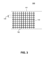
- Fig. 3 is a detailed view of a protection device 100 including a plate 101 and a mesh 102 attached to the plate 101, according to a typical embodiment.
- the protection device 100 includes the plate 101 and has the mesh 102 disposed over at least portions of the plate 101.
- the mesh 102 faces the substrate (not shown in Fig. 3 ).
- the mesh 102 may have a predetermined mesh spacing 104 such that a number of recesses 103 of predetermined sizes are obtained. Within the recesses, and at the mesh 102 and the plate 101, respectively, excess deposition material evaporated from the deposition source 301 may be retained, e.g. as particles or in liquid form.
- the plate 101 may have a corrugated surface in order to enhance a retainment of excess deposition material evaporated from the deposition source 301.
- an interval of the corrugations may correspond to the mesh spacing 104 such that even deeper recesses are obtained which may receive excess deposition material.
- the plate 101 of the protection device 100 may include a material which is selected from the group consisting of steel, copper, aluminium, bronze, an alloy and any combination thereof.
- the mesh 102 may be designed such that the mesh spacing 104 is in a range from 1 mm to 5 cm, and typically amounts to approximately 1 cm.
- the plate may not be fully covered by the mesh 102, i.e. the mesh 102 may be disposed at predetermined portions of the plate 101, wherein remaining portions of the plate 101 may not be covered by the mesh.
- the mesh 102 may be provided at the plate 101 such that the plate 101 is fully covered by the mesh 102.
- the plate 101 and the mesh 102 may be formed as an integral unit, i.e. the integral unit may include the plate 101 fully covered by the mesh 102 or the plate 101 not fully covered by the mesh 102.
- At least one of the plate 101 and the mesh 102 may be formed of a heat-resistant material.
- the plate 101 may include a material which is selected from the group consisting of steel, copper, aluminium, brass, an alloy and any combination thereof.
- the mesh 102 may include a material which is selected from the group consisting of steel, copper, aluminium, brass, an alloy and any combination thereof.
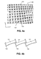
- Fig. 4a is an elevated perspective view showing a protection device in accordance with a typical embodiment.
- a wire mesh 102 is arranged at a side of the plate 101.
- a number of recesses 103 are formed where excess deposition material 200 evaporated by the deposition source 301 may be retained.
- the mesh 102 may be a plaited mesh, wherein the area covered by the mesh 102 may coincide with the area of the plate 101 or may be less than the area of the plate 101 such that portions of the plate 101 are not covered by the mesh 102.
- the mesh spacing 104 may vary along the plate in an x-direction and/or in a y-direction shown in Fig. 4a .
- the recess sizes may be adapted to an expected amount of deposition material to be received by the plate-mesh 101, 102 structure.
- the shape of the recesses 103 may be a square as shown in Fig. 4a , but other shapes may also be applied.
- the mesh may be formed by plated wires.
- the mesh 102 may be bonded at the plate 101 at the side of the plate 101 facing the substrate 302.
- An issue when designing the protection device 100 is the support of the mesh 102 at the plate 101.
- the mesh In order to avoid overheating of the mesh 102 the mesh is attached as close as possible at the plate, i.e. a good thermal contact is provided.
- the evaporation rate at the deposition source 301 is set at high values.
- the mesh 102 may be heated by condensation heat such that the protection device may represent an additional heat source for the substrate 301. In case the mesh 102 has been heated up to excessive temperatures, e.g. due to a long duration of the deposition process and/or interruption of substrate supply, evaporation times and excess deposition material may drop off the mesh 102.
- the mesh 102 is closely attached at the plate 101, e.g. by means of additional fixing points which may be provided in the form of bolt heads. It is noted here that these fixing points may be designed such that they are not acting as additional particle sources. The fixing points may be arranged such that a sufficient thermal contact between the mesh 102 and the respective plate 101 is provided.
- Fig. 4b is a side sectional view of three plates 101 having meshes 102 disposed thereon.
- an individual mesh 102 has a curved shape wherein a convex side of the mesh 102 may touch the plate 101 at the side of the plate 101 facing the substrate 302.
- the curved shape of the mesh 102 provides a mechanical pre-stress for an increased thermal contact of the mesh 102 with the surface of the respective plate 101.
- An increased thermal contact between mesh 102 and plate surface provides an effective cooling of the mesh 102, and thus excess deposition material may be held at the protection device 100 in a more reliable manner.
- the individual meshes 102 may be shaped such that they can be drawn over the respective plate 101 from a side of the plate 101.
- an easy installation of an individual mesh 102 at the corresponding plate 101 may be provided.
- the individual plates 101 having the meshes 102 disposed thereon may partially overlap in a roofing tile-manner as illustrated in the side sectional view of Fig. 4b . In this way a quasi-continuous coating of excess deposition material at meshes 102 belonging to adjacent plates 101 without rated break point within the deposited coating may be achieved.
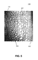
- Fig. 5 depicts a protection device 100 which has been subjected to excess evaporation material 200 evaporated by the deposition source 301. As shown in Fig. 5 , portions of the protection device 100 are coated by excess deposition material, i.e. retained deposition material 201 can be observed in specific regions of the plate-mesh 101, 102 arrangement, e.g. in liquid or solid form.
- the mesh spacing 104 (see Fig. 3 ) is designed such that a dropping-down of deposition material is reduced.
- the received part of deposition material 200 i.e. the excess deposition material is retained at at least one of the plate 101 and the mesh 102 as particles or in liquid form. Evaporation rates which may be provided within the process chamber 300 thus may be increased without damaging the substrate by drop-down of excess deposition material.
- dynamic deposition rates ranging from 0.01 ⁇ m x m/min to 50 ⁇ m x m/min, and typically of approximately 5 ⁇ m x m/min, may be provided within the process chamber 300 without substrate damage.
- Fig. 6 is a flowchart illustrating a method for depositing a thin film onto a substrate 302 within a process chamber 300. The procedure starts at a block 401. At a block 402, the substrate 302 is arranged in the process chamber 300. Then deposition material 200 is generated in a gas phase within the process chamber 300 (block 403).
- generated deposition material i.e. film-forming deposition material 200
- the substrate 302 for forming the thin film.
- At least another part of the generated deposition material 200, i.e. the excess deposition material, is received at the plate 101 having the mesh 102 disposed thereon (block 405).
- the procedure is ended at a block 406.
- a protection device adapted for protecting substrates within a process chamber against deposition material generated by a deposition source
- the protection device including a plate adapted for facing the substrate at a side opposing the deposition source; and a mesh disposed over the plate, the mesh facing the substrate.
- the plate includes a temperature control means adapted for controlling the temperature of the plate.
- the temperature control means may include cooling channels adapted for receiving a cooling fluid.
- the mesh is formed by plated wires.
- a mesh spacing of the mesh is in a range from 1 mm to 5 cm, and typically amounts to approximately 1 cm.
- the mesh spacing varies along the plate.
- the mesh is disposed at predetermined portions of the plate, wherein remaining portions of the plate are not covered by the mesh.
- the mesh may be bonded at the plate at the side of the plate facing the substrate.
- the plate and the mesh are formed as an integral unit.
- at least one of the plate and the wire mesh are formed of a heat resistant material.
- the plate may include a material which is selected from the group consisting of steel, copper, aluminum, brass, an alloy and any combination thereof.
- the wire mesh may include a material which is selected from the group consisting of steel, copper, aluminum, brass, an alloy and any combination thereof.
- the plate includes a heating unit adapted for heating the plate.
- a method is provided for depositing, within a process chamber, a thin film onto a substrate, the method including arranging the substrate in the process chamber; generating deposition material in a gas phase, within the process chamber; depositing, from the gas phase, at least a part of the generated depositing material onto the substrate for forming the thin film; and receiving at least another part of the generated deposition material at a plate having a mesh disposed thereon.
- the method may further include arranging the plate in the vicinity of a deposition source generating the deposition material, the mesh facing the deposition source.
- the deposition material is generated at an evaporation rate which is in a range from 0.01 ⁇ m x m/min to 30 ⁇ m x m/min, and typically amounts to approximately 5.0 ⁇ m x m/min.
- the received part of the generated deposition material is retained at at least one of the plate and the mesh as particles or in liquid form.
- the temperature of the plate may be controlled using a temperature control means.
- the temperature of the plate may be controlled by flowing a cooling fluid through cooling channels provided in the plate.
- the temperature of the plate is controlled by heating the plate by means of a heating unit.
Landscapes
- Chemical & Material Sciences (AREA)
- Chemical Kinetics & Catalysis (AREA)
- Engineering & Computer Science (AREA)
- Materials Engineering (AREA)
- Mechanical Engineering (AREA)
- Metallurgy (AREA)
- Organic Chemistry (AREA)
- General Chemical & Material Sciences (AREA)
- Photovoltaic Devices (AREA)
- Physical Vapour Deposition (AREA)
Priority Applications (2)
| Application Number | Priority Date | Filing Date | Title |
|---|---|---|---|
| EP10153066A EP2354271A1 (fr) | 2010-02-09 | 2010-02-09 | Dispositif et procédé de protection de substrat |
| US12/705,765 US20110195184A1 (en) | 2010-02-09 | 2010-02-15 | Substrate protection device and method |
Applications Claiming Priority (1)
| Application Number | Priority Date | Filing Date | Title |
|---|---|---|---|
| EP10153066A EP2354271A1 (fr) | 2010-02-09 | 2010-02-09 | Dispositif et procédé de protection de substrat |
Publications (1)
| Publication Number | Publication Date |
|---|---|
| EP2354271A1 true EP2354271A1 (fr) | 2011-08-10 |
Family
ID=42290268
Family Applications (1)
| Application Number | Title | Priority Date | Filing Date |
|---|---|---|---|
| EP10153066A Withdrawn EP2354271A1 (fr) | 2010-02-09 | 2010-02-09 | Dispositif et procédé de protection de substrat |
Country Status (2)
| Country | Link |
|---|---|
| US (1) | US20110195184A1 (fr) |
| EP (1) | EP2354271A1 (fr) |
Cited By (1)
| Publication number | Priority date | Publication date | Assignee | Title |
|---|---|---|---|---|
| CN103122451A (zh) * | 2013-02-05 | 2013-05-29 | 吴江南玻华东工程玻璃有限公司 | 可摇动式l型包网挡板 |
Families Citing this family (2)
| Publication number | Priority date | Publication date | Assignee | Title |
|---|---|---|---|---|
| KR102075527B1 (ko) * | 2013-05-16 | 2020-02-11 | 삼성디스플레이 주식회사 | 유기층 증착 장치 및 이를 이용한 유기 발광 디스플레이 장치의 제조 방법 |
| CN112301312A (zh) * | 2019-07-25 | 2021-02-02 | 杭州纤纳光电科技有限公司 | 蒸镀装置及其蒸镀原料的回收方法 |
Citations (5)
| Publication number | Priority date | Publication date | Assignee | Title |
|---|---|---|---|---|
| JPS6130661A (ja) * | 1984-07-19 | 1986-02-12 | Matsushita Electric Ind Co Ltd | 被膜形成装置 |
| JPS62202075A (ja) * | 1986-02-28 | 1987-09-05 | Toshiba Corp | 薄膜形成装置 |
| US5080774A (en) * | 1986-10-11 | 1992-01-14 | Saint-Gobain Vitrage | Surface configuration means for vacuum coating device |
| US20020069970A1 (en) * | 2000-03-07 | 2002-06-13 | Applied Materials, Inc. | Temperature controlled semiconductor processing chamber liner |
| US20070234959A1 (en) * | 2006-04-05 | 2007-10-11 | Seiko Epson Corporation | Evaporation apparatus, evaporation method, method of manufacturing electro-optical device, and film-forming apparatus |
Family Cites Families (3)
| Publication number | Priority date | Publication date | Assignee | Title |
|---|---|---|---|---|
| JP3744964B2 (ja) * | 1995-04-06 | 2006-02-15 | 株式会社アルバック | 成膜装置用構成部品及びその製造方法 |
| WO1998031845A1 (fr) * | 1997-01-16 | 1998-07-23 | Bottomfield, Layne, F. | Composants pour metallisation par evaporation sous vide et procedes correspondants |
| JP4430506B2 (ja) * | 2004-10-14 | 2010-03-10 | 三菱電機株式会社 | 蒸着装置 |
-
2010
- 2010-02-09 EP EP10153066A patent/EP2354271A1/fr not_active Withdrawn
- 2010-02-15 US US12/705,765 patent/US20110195184A1/en not_active Abandoned
Patent Citations (5)
| Publication number | Priority date | Publication date | Assignee | Title |
|---|---|---|---|---|
| JPS6130661A (ja) * | 1984-07-19 | 1986-02-12 | Matsushita Electric Ind Co Ltd | 被膜形成装置 |
| JPS62202075A (ja) * | 1986-02-28 | 1987-09-05 | Toshiba Corp | 薄膜形成装置 |
| US5080774A (en) * | 1986-10-11 | 1992-01-14 | Saint-Gobain Vitrage | Surface configuration means for vacuum coating device |
| US20020069970A1 (en) * | 2000-03-07 | 2002-06-13 | Applied Materials, Inc. | Temperature controlled semiconductor processing chamber liner |
| US20070234959A1 (en) * | 2006-04-05 | 2007-10-11 | Seiko Epson Corporation | Evaporation apparatus, evaporation method, method of manufacturing electro-optical device, and film-forming apparatus |
Cited By (1)
| Publication number | Priority date | Publication date | Assignee | Title |
|---|---|---|---|---|
| CN103122451A (zh) * | 2013-02-05 | 2013-05-29 | 吴江南玻华东工程玻璃有限公司 | 可摇动式l型包网挡板 |
Also Published As
| Publication number | Publication date |
|---|---|
| US20110195184A1 (en) | 2011-08-11 |
Similar Documents
| Publication | Publication Date | Title |
|---|---|---|
| KR101077046B1 (ko) | 신규한 금속 스트립 제품 | |
| US20100248416A1 (en) | Deposition of high vapor pressure materials | |
| US20100140078A1 (en) | Method and apparatus for forming contact layers for continuous workpieces | |
| KR20090026125A (ko) | 대형 기판 상에 아연 산화물 투명 전도성 산화물의 반응성 스퍼터링 | |
| WO2009055125A3 (fr) | Système de protection contre le gel et procédé pour amplifier le transfert de chaleur | |
| US20120021556A1 (en) | Deposition system | |
| US20090061627A1 (en) | Method for producing a metal backside contact of a semiconductor component, in particular, a solar cell | |
| EP3559303A1 (fr) | Source d'évaporation linéaire | |
| CN208136329U (zh) | 一种带防液滴喷溅格栅的热蒸发装置 | |
| JP5346239B2 (ja) | 真空蒸着装置 | |
| EP2507402A1 (fr) | Source de déposition linéaire | |
| KR20140126323A (ko) | 광발전 전지용 보호 코팅 | |
| EP2354271A1 (fr) | Dispositif et procédé de protection de substrat | |
| EP3559305A1 (fr) | Système de dépôt en phase vapeur de rouleau à rouleau | |
| WO2011084292A3 (fr) | Cellule photovoltaïque sous forme d'un film mince de silicium ayant un niveau de flou amélioré et ses procédés de fabrication | |
| US5487786A (en) | Plasma chemical vapor deposition device capable of suppressing generation of polysilane powder | |
| CN103890975B (zh) | 液体靶材的溅射系统 | |
| JP4703782B2 (ja) | 半導体構成要素、特にソーラーセルの金属裏側コンタクトの製造方法 | |
| EP3559304A1 (fr) | Source de vapeur linéaire | |
| WO2006077986A1 (fr) | Dispositif de formation d'un film conducteur transparent, dispositif de formation en continu d'un film conducteur transparent multicouche et procede de formation d'un film a l'aide de ce dernier | |
| WO2013039862A2 (fr) | Procédés de dépôt de matériaux composites métal-polymère sur un substrat | |
| US20100035432A1 (en) | Chemical vapor deposition method and system for semiconductor devices | |
| CN117677728A (zh) | 用于物理气相沉积卷材涂覆的封闭耦接扩散器 | |
| WO2011065998A1 (fr) | Source de déposition linéaire | |
| US20100236920A1 (en) | Deposition apparatus with high temperature rotatable target and method of operating thereof |
Legal Events
| Date | Code | Title | Description |
|---|---|---|---|
| PUAI | Public reference made under article 153(3) epc to a published international application that has entered the european phase |
Free format text: ORIGINAL CODE: 0009012 |
|
| AK | Designated contracting states |
Kind code of ref document: A1 Designated state(s): AT BE BG CH CY CZ DE DK EE ES FI FR GB GR HR HU IE IS IT LI LT LU LV MC MK MT NL NO PL PT RO SE SI SK SM TR |
|
| STAA | Information on the status of an ep patent application or granted ep patent |
Free format text: STATUS: THE APPLICATION IS DEEMED TO BE WITHDRAWN |
|
| 18D | Application deemed to be withdrawn |
Effective date: 20120211 |