EP2355340B1 - Filtre passe-bas analogique à large bande - Google Patents
Filtre passe-bas analogique à large bande Download PDFInfo
- Publication number
- EP2355340B1 EP2355340B1 EP11250107.7A EP11250107A EP2355340B1 EP 2355340 B1 EP2355340 B1 EP 2355340B1 EP 11250107 A EP11250107 A EP 11250107A EP 2355340 B1 EP2355340 B1 EP 2355340B1
- Authority
- EP
- European Patent Office
- Prior art keywords
- filter
- coupled
- capacitor
- inductors
- inductor
- Prior art date
- Legal status (The legal status is an assumption and is not a legal conclusion. Google has not performed a legal analysis and makes no representation as to the accuracy of the status listed.)
- Active
Links
Images


Classifications
-
- H—ELECTRICITY
- H03—ELECTRONIC CIRCUITRY
- H03J—TUNING RESONANT CIRCUITS; SELECTING RESONANT CIRCUITS
- H03J3/00—Continuous tuning
- H03J3/20—Continuous tuning of single resonant circuit by varying inductance only or capacitance only
-
- H—ELECTRICITY
- H01—ELECTRIC ELEMENTS
- H01P—WAVEGUIDES; RESONATORS, LINES, OR OTHER DEVICES OF THE WAVEGUIDE TYPE
- H01P1/00—Auxiliary devices
- H01P1/20—Frequency-selective devices, e.g. filters
- H01P1/201—Filters for transverse electromagnetic waves
- H01P1/203—Strip line filters
- H01P1/20327—Electromagnetic interstage coupling
- H01P1/20354—Non-comb or non-interdigital filters
- H01P1/20381—Special shape resonators
-
- H—ELECTRICITY
- H03—ELECTRONIC CIRCUITRY
- H03H—IMPEDANCE NETWORKS, e.g. RESONANT CIRCUITS; RESONATORS
- H03H7/00—Multiple-port networks comprising only passive electrical elements as network components
- H03H7/01—Frequency selective two-port networks
- H03H7/0153—Electrical filters; Controlling thereof
-
- H—ELECTRICITY
- H03—ELECTRONIC CIRCUITRY
- H03H—IMPEDANCE NETWORKS, e.g. RESONANT CIRCUITS; RESONATORS
- H03H7/00—Multiple-port networks comprising only passive electrical elements as network components
- H03H7/01—Frequency selective two-port networks
- H03H7/06—Frequency selective two-port networks including resistors
Definitions
- the invention relates to a lowpass filter.
- Lowpass filters are known in the art.
- One type of a lowpass filter is a Chebyshev filter that uses fixed values for its inductors and capacitors. Once the fixed values of the inductors and capacitors are selected, the cutoff frequency of the filter cannot typically be varied without changing components.
- U.S. Patent Publ. No. 2005/0134398 discloses a tunable high-order Bessel low pass filter that includes two tunable inductors VL1 and VL2.
- the 398 publication fails to disclose a low pass filter that provides adequate out of band rejection.
- a low pass filter having high linearity and which has a tunable cutoff frequency can be achieved by a plurality of inductors coupled in series between RF input and output terminals, and at least one electrically tunable capacitor coupled to a node of one of the inductors, in which each of the inductors includes a winding, and a resistance and a capacitance coupled in series across a portion of the winding to enhance the out of band rejection of the low pass filter.
- the subject invention features a low pass filter which includes an RF input terminal; an RF output terminal; a plurality of inductors coupled in series between the RF input and output terminals; and at least one electrically tunable capacitor coupled to a node of one of the inductors; at least one of the inductors including a winding that includes a first end, a second end and a pair of nodes defining a portion of the winding between the first end and the second end, and a combination of resistor and a capacitor coupled in series the resistor and the capacitor combination being coupled in parallel with the portion of the winding defined by the pair of nodes to enhance the out of band rejection of the low pass filter.
- the resistance and the capacitance are coupled in series between two nodes that have a phase difference of approximately 180 degrees at a frequency at which the inductor becomes resonant.
- a magnimde of a reactance of the capacitance may be approximately equal to a value of the resistor at the resonant frequency of the inductor.
- the electrically tunable capacitors may each include a varactor.
- Each of the varactors may include two diodes coupled together anode to anode or cathode to cathode.
- Each of the varactors may alternatively include one diode.
- Each of the varactors may include a p-n junction.
- Each of the varactors may include a field effect transistor (FET) and use the capacitance between a gate and a source of the FET.
- FET field effect transistor
- Each electrically tunable capacitor may include a ferroelectric based capacitor.
- Each electrically tunable capacitor may include a MEMS-based capacitor.
- the electrically tunable capacitors may be coupled between ground and the node of one of the inductors.
- the filter may also include a control circuit coupled to the electrically tunable capacitors to adjust the cut off frequency of the falter.
- the control circuit may include a frequency control terminal, and an inductance and a resistance coupled in series between the frequency control terminal and each of the tunable capacitors for tuning the tunable capacitors.
- the filter may be implemented on a planar monolithic substrate.
- the monolithic substrate may be selected from the group of GaAs or SiGe.
- the monolithic substrate may be mounted in a surface-mount package.
- Each of the inductors may be a lumped inductor.
- Each of the inductors may be a spiral inductor.
- the subject invention features a low pass filter which includes an RF input terminal; an RF output terminal; a plurality of inductors coupled in series between the RF input and output terminals; at least one electrically tunable capacitor coupled between ground and a node of one of the inductors; and a control circuit coupled to the electrically tunable capacitors of the resonating circuits to adjust the cut off frequency of the filter; each of the inductors including a winding, and a resistance and a capacitance coupled in series across two nodes of the winding that have a phase difference of approximately 180 degrees at a frequency at which the inductor becomes resonant to enhance the out of band rejection of the low pass filter.
- the plurality of electrically tunable capacitors each includes a varactor.
- Each of the varactors may include two diodes coupled together anode to anode or cathode to cathode.
- Each of the varactors may include one diode.
- an inductor in another embodiment, includes a winding, and a resistance and a capacitance coupled in series across a portion of the winding to enhance the out of band rejection of the inductor, the resistance and the capacitance coupled in series between two nodes of the winding that have a phase difference of approximately 180 degrees at a frequency at which the inductor becomes resonant.
- the magnitude of a reactance of the capacitance may be approximately equal to a value of the resistor at the resonant frequency of the inductor.
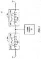
- a wideband analog lowpass filter 10 in accordance with the invention that includes an RF input terminal 12, an RF output terminal 14, and a plurality of inductors 16a-b coupled in series between the RF input and output terminals. At least one electrically tunable capacitor 18 is coupled to a node of one of inductors 16a-b.
- Each of the inductors 16a-b respectively includes a winding 20a-b, and a resistance 22a-b and a capacitance 24a-b coupled in series across a portion of the winding to enhance the out of band rejection of the low pass filter.
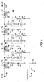
- FIG. 2 Another embodiment of wideband analog lowpass filter 10a, Fig. 2 , takes the configuration of a seventh-order lumped element Chebyshev filter.
- Filter 10a includes back to back varactors 18a-18c to provide electrically tunable capacitance. Although single varactors may be used, the back to back varactors provide improved linearity performance over a single varactor implementation.
- a control circuit 26 is coupled to the pairs of tunable varactors 18a-18c to adjust the cut off frequency of the filter.
- Control circuit 26 includes a frequency control terminal 28, and inductors 30a-c and resistors 32a-c coupled in series between the frequency control terminal and the cathodes of each of the pairs of tunable varactors 18a-18c for tuning the varactors.
- Inductor 33a-c and resistors 31a-c also provide a dc return for some of the anodes of the pairs of varactors 18a-18c that are not already directly grounded.
- the pairs of varactors 18a-18c are respectively ac coupled to inductors 16a-c through capacitors 34a-c.
- the reactance of capacitors 34a-c are respectively very small compared to the reactance of the pairs of back to back varactors 18a-18c.
- Inductors 16c-f have embedded resistors 22c-f and capacitors 24c-fwhich provide significant additional out of band rejection in the frequency range where distributed circuit effects, such as parasitic capacitance inherent in the physical layout of the inductors typically don't provide the lumped element equivalent inductance as was the case in the frequency range of the pass band.
- Inductors 16c-f may be implemented as lumped inductors and/or as planar spiral inductors.
- filter 10a includes four inductors 16c-f
- the subject invention could include any number of inductors.
- one embodiment of the invention includes a single inductor 16a having a winding 20a, and a resistance 22a and a capacitance 24a coupled in series across a portion of the winding to enhance the out of band rejection of the inductor.
- Filter 10a could also take the configuration of any type of filter topology which incorporates lumped element equivalent inductors, such as for example, Butterworth, Eliptic, Bessel, Cauer filters, etc.
- the linearity of filter 10a is improved by incorporating back to back pairs of varactors in the filter substantially eliminating the non-symmetrical variation of capacitance under ac excitation around a given dc operating point.
- the back to back pairs of varactors 18a-c in Fig. 2 are shown coupled as cathode to cathode, but each may alternatively be coupled as anode to anode.
- Other electrically tunable capacitors could be used instead of back to back pairs of tunable varactors 18a-18c, such as a single varactor, a ferroelectric based capacitor, a MEMS-based capacitor, and/or a field effect transistor (FET) that uses the capacitance between the gate and the source of the FET.
- FET field effect transistor
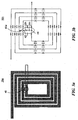
- a layout, Fig. 3a , of one embodiment of inductor 16g shows an exemplary location of the resistor and capacitor 40 within inductor 16g.
- the location of the resistor and capacitor 40 is dependent on the inductor layout and may be determined by examination of a finite element analysis of the structure showing the electromagnetic field distribution.
- the resistor and capacitor 40 are preferably placed between nodes which have a phase difference of approximately 180 degrees at the frequency where inductor 16g becomes resonant. This has the desirable effect of absorbing the energy in the frequency range where the inductor is resonant while having only a very small effect on the performance of inductor 16g (and in turn filter 10a) in the frequency range of the pass band.
- 3b shows the equivalent low frequency lumped element inductor model 16h of inductor 16g which illustrates an example of resistor 22h and capacitor 24h coupled in series across a portion of the inductor winding between nodes 42 and 44 to enhance the out of band rejection of the low pass filter.
- the magnitude of the reactance of the capacitor 24h is approximately equal to the value of resistor 22h at the resonant frequency of the inductor. This helps to ensure that there is minimal impact to the performance of the inductor in the passband.
- the filter may be implemented on a planar monolithic substrate which for example may be a GaAs or SiGe substrate.
- the response 60, Fig. 5 , of the lowpass filter 10a shows the insertion loss of the lowpass filter as the tuning voltage applied to the cathodes of varactors 18a-c is varied across the range of 0 to 14 volts.
- the corner or cutoff frequency 62 of filter 10a tunes from 2 GHz to 4 GHz.
- the 60 dB stop band 64 of this filter extends to 24 GHz and the out of band rejection 66 is still 30 dB at 30 GHz.
- Embodiments of the invention provide a lowpass filter which has a tunable cutoff frequency and has high linearity such that a minimal amount of additional spurious are generated when subjected to an input spectrum with multiple tones.
- the out of band rejection may remain high and extend several octaves or more beyond the initial stop band to insure that spurious far from carrier do not re-enter the system in some non obvious fashion. This performance may be achieved with relatively low and flat insertion loss.
- Embodiments of the invention may also be realized on a monolithic substrate to benefit from the consistency of the many reactive elements, reduced size, low cost, and the possibility to integrate other active or passive circuit functions on the same die.
Landscapes
- Physics & Mathematics (AREA)
- Electromagnetism (AREA)
- Filters And Equalizers (AREA)
- Networks Using Active Elements (AREA)
Claims (15)
- Filtre passe-bas (10) ayant une borne d'entrée RF (12) et une borne de sortie RF (14), le filtre passe-bas comportant :- une pluralité d'inducteurs (16a-b) couplés en série entre les bornes d'entrée et de sortie RF ; et- au moins un condensateur accordable électriquement (18) couplé à un noeud d'un des inducteurs ; le filtre passe-bas étant caractérisé en ce quechacun des inducteurs comporte un enroulement (20a-b) qui présente une première extrémité, une seconde extrémité et une paire de noeuds (42, 44) définissant une partie de l'enroulement entre la première extrémité et la seconde extrémité, et une combinaison d'une résistance (22a-b) et d'un condensateur (24a-b) couplés en série, la combinaison de la résistance et du condensateur étant couplée en parallèle avec la partie de l'enroulement définie par la paire de noeuds pour l'arrêt hors-bande du filtre passe-bas.
- Filtre selon la revendication 1, dans lequel la résistance et le condensateur sont couplés en série entre deux noeuds qui ont une différence de phase d'environ 180 degrés à une fréquence à laquelle l'inducteur devient résonant.
- Filtre selon la revendication 1, dans lequel la pluralité de condensateurs électriquement accordables comporte chacun un varactor (18a-18c).
- Filtre selon la revendication 3, dans lequel chacun des varactors comporte deux diodes couplées ensemble anode à d'anode ou de cathode à cathode.
- Filtre selon la revendication 1, comportant en outre un circuit de contrôle (26) couplé aux condensateurs accordables électriquement pour ajuster la fréquence de coupure du filtre.
- Filtre selon la revendication 5, dans lequel le circuit de contrôle comporte une borne de contrôle de fréquence (28) ainsi qu'un inducteur (30a-c) et une résistance (32a-c) couplés en série entre la borne de contrôle de fréquence et chacun des condensateurs accordables pour accorder les condensateurs accordables.
- Filtre selon la revendication 1 dans lequel le filtre est mis en oeuvre sur un substrat monolithique planaire.
- Filtre selon la revendication 3 dans lequel chacun des varactors comporte une jonction p-n.
- Filtre selon la revendication 3 dans lequel chacun des varactors comporte un transistor à effet de champ (FET) et utilise un condensateur entre une porte et une source du FET.
- Filtre selon la revendication 1 dans lequel chaque condensateur électriquement accordable comporte un condensateur à base ferroélectrique.
- Filtre selon la revendication 1 dans lequel chaque condensateur électriquement accordable comporte un condensateur à base MEMS.
- Filtre selon la revendication 7 dans lequel le substrat monolithique est monté dans un boîtier de montage en surface.
- Filtre selon la revendication 1 dans lequel chacun des inducteurs est un inducteur spiral.
- Filtre selon la revendication 1 dans lequel l'au moins un condensateur électriquement accordable est couplé entre la terre et le noeud de l'un des inducteurs.
- Filtre selon la revendication 1 dans lequel une magnitude d'une réactance du condensateur de l'inducteur est approximativement égale à une valeur de la résistance à la fréquence de résonance de l'inducteur.
Applications Claiming Priority (1)
| Application Number | Priority Date | Filing Date | Title |
|---|---|---|---|
| US33751510P | 2010-02-04 | 2010-02-04 |
Publications (2)
| Publication Number | Publication Date |
|---|---|
| EP2355340A1 EP2355340A1 (fr) | 2011-08-10 |
| EP2355340B1 true EP2355340B1 (fr) | 2016-11-09 |
Family
ID=43928861
Family Applications (1)
| Application Number | Title | Priority Date | Filing Date |
|---|---|---|---|
| EP11250107.7A Active EP2355340B1 (fr) | 2010-02-04 | 2011-02-01 | Filtre passe-bas analogique à large bande |
Country Status (3)
| Country | Link |
|---|---|
| US (1) | US8928431B2 (fr) |
| EP (1) | EP2355340B1 (fr) |
| CN (1) | CN102148610B (fr) |
Families Citing this family (13)
| Publication number | Priority date | Publication date | Assignee | Title |
|---|---|---|---|---|
| JP5752803B2 (ja) * | 2010-12-23 | 2015-07-22 | クゥアルコム・テクノロジーズ・インコーポレイテッド | Rf装置およびrf装置のチューニング方法 |
| CN104602377B (zh) * | 2013-10-30 | 2017-03-08 | 美的集团股份有限公司 | 电磁炉和用于电磁炉的滤波电路及其的控制方法 |
| CN104202006A (zh) * | 2014-09-01 | 2014-12-10 | 王少夫 | 一种可调的简易低通滤波电路 |
| US9800134B2 (en) * | 2015-02-25 | 2017-10-24 | Rockwell Automation Technologies, Inc. | Motor drive with LCL filter inductor with built-in passive damping resistor for AFE rectifier |
| US9948265B2 (en) * | 2015-05-14 | 2018-04-17 | Mediatek Inc. | Inductor capacitor tank for resonator |
| JP2018113547A (ja) * | 2017-01-10 | 2018-07-19 | 株式会社村田製作所 | ローパスフィルタ |
| CN107070189A (zh) * | 2017-04-11 | 2017-08-18 | 北京北广科技股份有限公司 | 一种射频电源检波电路中的滤波电路 |
| US10622960B2 (en) * | 2017-10-17 | 2020-04-14 | Mitsubishi Electric Research Laboratories, Inc. | Filters with virtual inductor implemented using negative capacitor |
| CN108377138A (zh) * | 2018-01-10 | 2018-08-07 | 海能达通信股份有限公司 | 一种带通滤波器及接收机 |
| CN108259021A (zh) * | 2018-01-10 | 2018-07-06 | 广西师范大学 | 一种cmos宽带分布式可调带通滤波器 |
| US10522889B2 (en) | 2018-04-09 | 2019-12-31 | United States Of America As Represented By Secretary Of The Navy | Tunable passive enhance Q microwave notch filter |
| EP3588559B1 (fr) * | 2018-06-29 | 2021-10-20 | Intel Corporation | Circuit de protection contre les décharges électrostatiques pour des interfaces multibandes à large plage de fréquences |
| US11716066B2 (en) | 2020-12-16 | 2023-08-01 | KYOCERA AVX Components Corporation | Compact, high-power thin-film filter |
Family Cites Families (13)
| Publication number | Priority date | Publication date | Assignee | Title |
|---|---|---|---|---|
| NL278982A (fr) * | 1961-10-06 | |||
| US5032808A (en) * | 1989-07-21 | 1991-07-16 | Prabhakara Reddy | R.F. choke for CATV system |
| US5173681A (en) * | 1990-09-18 | 1992-12-22 | Quantum Engineering, Inc. | Speed sensitive visual warning system for locomotives |
| US5173671A (en) | 1990-12-18 | 1992-12-22 | Raytheon Company | Monolithic lumped element networks |
| JPH10209714A (ja) * | 1996-11-19 | 1998-08-07 | Sharp Corp | 電圧制御通過帯域可変フィルタおよびそれを用いる高周波回路モジュール |
| US5959515A (en) * | 1997-08-11 | 1999-09-28 | Motorola, Inc. | High Q integrated resonator structure |
| FR2798237B1 (fr) * | 1999-09-07 | 2002-05-03 | Itis | Dispositif de filtrage commande en frequence pour la bande uhf |
| US6850106B1 (en) * | 2003-07-08 | 2005-02-01 | Mohan Krishna Kunanayagam | Voltage controlled oscillator delay cell |
| KR100563661B1 (ko) | 2003-12-18 | 2006-03-23 | 한국전자통신연구원 | 가변 고차 베셀 저역 통과 필터 |
| US7305223B2 (en) * | 2004-12-23 | 2007-12-04 | Freescale Semiconductor, Inc. | Radio frequency circuit with integrated on-chip radio frequency signal coupler |
| US7679473B2 (en) | 2008-01-15 | 2010-03-16 | California Micro Devices | Low pass filter incorporating coupled inductors to enhance stop band attenuation |
| TWI350655B (en) | 2008-03-20 | 2011-10-11 | Ind Tech Res Inst | Circuit device with inductor and capacitor in parallel connection |
| US8305164B1 (en) * | 2009-06-09 | 2012-11-06 | The United States Of America, As Represented By The Secretary Of The Navy | Frequency-agile frequency-selective variable attenuator |
-
2011
- 2011-02-01 CN CN201110093892.0A patent/CN102148610B/zh active Active
- 2011-02-01 EP EP11250107.7A patent/EP2355340B1/fr active Active
- 2011-02-01 US US12/931,499 patent/US8928431B2/en active Active
Non-Patent Citations (1)
| Title |
|---|
| None * |
Also Published As
| Publication number | Publication date |
|---|---|
| CN102148610B (zh) | 2016-01-27 |
| US8928431B2 (en) | 2015-01-06 |
| US20110187449A1 (en) | 2011-08-04 |
| CN102148610A (zh) | 2011-08-10 |
| EP2355340A1 (fr) | 2011-08-10 |
Similar Documents
| Publication | Publication Date | Title |
|---|---|---|
| EP2355340B1 (fr) | Filtre passe-bas analogique à large bande | |
| EP2355349B1 (fr) | Filtre passe-bande analogique à bande large | |
| EP2387095B1 (fr) | Filtre en peigne | |
| US8525620B2 (en) | BAW resonator filter bandwidth and out-of-band frequency rejection | |
| Lucyszyn et al. | Monolithic narrow-band filter using ultrahigh-Q tunable active inductors | |
| CN101894995B (zh) | 一种具有恒定绝对带宽的射频电调带通滤波器 | |
| US9154104B2 (en) | Miniaturized passive low pass filter | |
| CN101473488B (zh) | 用于多频带射频耦合的pin二极管网络 | |
| US6806793B2 (en) | MLC frequency selective circuit structures | |
| US6768383B2 (en) | High-frequency amplifier | |
| CN111697939B (zh) | 一种可重构带阻滤波器 | |
| US6255913B1 (en) | Variable frequency oscillator circuit | |
| US20210344319A1 (en) | Interdigitated rf filter | |
| US6781482B2 (en) | Integrated circuit | |
| Bhat et al. | Electronically tunable dual band microwave filter | |
| CN221862820U (zh) | 一种电调射频滤波器电路 | |
| TWI803091B (zh) | 雙工器 | |
| CN121585133B (zh) | 一种高邻带抑制的大带宽滤波器 | |
| Zhu et al. | Active Tunable Bandpass Filter based on Distributed Amplification | |
| CN113037239A (zh) | 滤波器和电子设备 | |
| EP2306636B1 (fr) | Circuit résonant pour des oscillateurs à micro-ondes | |
| EP2362540B1 (fr) | Oscillateur de commande de tension à micro-ondes avec un rapport signal sur bruit amélioré | |
| JPH10284996A (ja) | 高速同調フィルタ | |
| JP2021170805A (ja) | フィルタおよび電子機器 | |
| KR20070112992A (ko) | 알에프 하모닉 주파수의 노치 회로 |
Legal Events
| Date | Code | Title | Description |
|---|---|---|---|
| PUAI | Public reference made under article 153(3) epc to a published international application that has entered the european phase |
Free format text: ORIGINAL CODE: 0009012 |
|
| 17P | Request for examination filed |
Effective date: 20110223 |
|
| AK | Designated contracting states |
Kind code of ref document: A1 Designated state(s): AL AT BE BG CH CY CZ DE DK EE ES FI FR GB GR HR HU IE IS IT LI LT LU LV MC MK MT NL NO PL PT RO RS SE SI SK SM TR |
|
| AX | Request for extension of the european patent |
Extension state: BA ME |
|
| REG | Reference to a national code |
Ref country code: DE Ref legal event code: R079 Ref document number: 602011032145 Country of ref document: DE Free format text: PREVIOUS MAIN CLASS: H03H0007010000 Ipc: H01P0001203000 |
|
| GRAP | Despatch of communication of intention to grant a patent |
Free format text: ORIGINAL CODE: EPIDOSNIGR1 |
|
| RIC1 | Information provided on ipc code assigned before grant |
Ipc: H01P 1/203 20060101AFI20160223BHEP Ipc: H03H 7/01 20060101ALI20160223BHEP Ipc: H03J 3/20 20060101ALI20160223BHEP Ipc: H03H 7/06 20060101ALI20160223BHEP |
|
| INTG | Intention to grant announced |
Effective date: 20160311 |
|
| GRAP | Despatch of communication of intention to grant a patent |
Free format text: ORIGINAL CODE: EPIDOSNIGR1 |
|
| INTG | Intention to grant announced |
Effective date: 20160616 |
|
| RAP1 | Party data changed (applicant data changed or rights of an application transferred) |
Owner name: HITTITE MICROWAVE LLC |
|
| GRAS | Grant fee paid |
Free format text: ORIGINAL CODE: EPIDOSNIGR3 |
|
| GRAA | (expected) grant |
Free format text: ORIGINAL CODE: 0009210 |
|
| AK | Designated contracting states |
Kind code of ref document: B1 Designated state(s): AL AT BE BG CH CY CZ DE DK EE ES FI FR GB GR HR HU IE IS IT LI LT LU LV MC MK MT NL NO PL PT RO RS SE SI SK SM TR |
|
| REG | Reference to a national code |
Ref country code: GB Ref legal event code: FG4D |
|
| REG | Reference to a national code |
Ref country code: AT Ref legal event code: REF Ref document number: 844668 Country of ref document: AT Kind code of ref document: T Effective date: 20161115 Ref country code: CH Ref legal event code: EP |
|
| REG | Reference to a national code |
Ref country code: IE Ref legal event code: FG4D |
|
| REG | Reference to a national code |
Ref country code: DE Ref legal event code: R096 Ref document number: 602011032145 Country of ref document: DE |
|
| PG25 | Lapsed in a contracting state [announced via postgrant information from national office to epo] |
Ref country code: LV Free format text: LAPSE BECAUSE OF FAILURE TO SUBMIT A TRANSLATION OF THE DESCRIPTION OR TO PAY THE FEE WITHIN THE PRESCRIBED TIME-LIMIT Effective date: 20161109 |
|
| REG | Reference to a national code |
Ref country code: LT Ref legal event code: MG4D |
|
| REG | Reference to a national code |
Ref country code: NL Ref legal event code: MP Effective date: 20161109 |
|
| REG | Reference to a national code |
Ref country code: AT Ref legal event code: MK05 Ref document number: 844668 Country of ref document: AT Kind code of ref document: T Effective date: 20161109 |
|
| PG25 | Lapsed in a contracting state [announced via postgrant information from national office to epo] |
Ref country code: LT Free format text: LAPSE BECAUSE OF FAILURE TO SUBMIT A TRANSLATION OF THE DESCRIPTION OR TO PAY THE FEE WITHIN THE PRESCRIBED TIME-LIMIT Effective date: 20161109 Ref country code: NL Free format text: LAPSE BECAUSE OF FAILURE TO SUBMIT A TRANSLATION OF THE DESCRIPTION OR TO PAY THE FEE WITHIN THE PRESCRIBED TIME-LIMIT Effective date: 20161109 Ref country code: GR Free format text: LAPSE BECAUSE OF FAILURE TO SUBMIT A TRANSLATION OF THE DESCRIPTION OR TO PAY THE FEE WITHIN THE PRESCRIBED TIME-LIMIT Effective date: 20170210 Ref country code: NO Free format text: LAPSE BECAUSE OF FAILURE TO SUBMIT A TRANSLATION OF THE DESCRIPTION OR TO PAY THE FEE WITHIN THE PRESCRIBED TIME-LIMIT Effective date: 20170209 Ref country code: SE Free format text: LAPSE BECAUSE OF FAILURE TO SUBMIT A TRANSLATION OF THE DESCRIPTION OR TO PAY THE FEE WITHIN THE PRESCRIBED TIME-LIMIT Effective date: 20161109 |
|
| PG25 | Lapsed in a contracting state [announced via postgrant information from national office to epo] |
Ref country code: PL Free format text: LAPSE BECAUSE OF FAILURE TO SUBMIT A TRANSLATION OF THE DESCRIPTION OR TO PAY THE FEE WITHIN THE PRESCRIBED TIME-LIMIT Effective date: 20161109 Ref country code: FI Free format text: LAPSE BECAUSE OF FAILURE TO SUBMIT A TRANSLATION OF THE DESCRIPTION OR TO PAY THE FEE WITHIN THE PRESCRIBED TIME-LIMIT Effective date: 20161109 Ref country code: BE Free format text: LAPSE BECAUSE OF NON-PAYMENT OF DUE FEES Effective date: 20170228 Ref country code: HR Free format text: LAPSE BECAUSE OF FAILURE TO SUBMIT A TRANSLATION OF THE DESCRIPTION OR TO PAY THE FEE WITHIN THE PRESCRIBED TIME-LIMIT Effective date: 20161109 Ref country code: AT Free format text: LAPSE BECAUSE OF FAILURE TO SUBMIT A TRANSLATION OF THE DESCRIPTION OR TO PAY THE FEE WITHIN THE PRESCRIBED TIME-LIMIT Effective date: 20161109 Ref country code: PT Free format text: LAPSE BECAUSE OF FAILURE TO SUBMIT A TRANSLATION OF THE DESCRIPTION OR TO PAY THE FEE WITHIN THE PRESCRIBED TIME-LIMIT Effective date: 20170309 Ref country code: RS Free format text: LAPSE BECAUSE OF FAILURE TO SUBMIT A TRANSLATION OF THE DESCRIPTION OR TO PAY THE FEE WITHIN THE PRESCRIBED TIME-LIMIT Effective date: 20161109 Ref country code: ES Free format text: LAPSE BECAUSE OF FAILURE TO SUBMIT A TRANSLATION OF THE DESCRIPTION OR TO PAY THE FEE WITHIN THE PRESCRIBED TIME-LIMIT Effective date: 20161109 Ref country code: IS Free format text: LAPSE BECAUSE OF FAILURE TO SUBMIT A TRANSLATION OF THE DESCRIPTION OR TO PAY THE FEE WITHIN THE PRESCRIBED TIME-LIMIT Effective date: 20170309 |
|
| PG25 | Lapsed in a contracting state [announced via postgrant information from national office to epo] |
Ref country code: RO Free format text: LAPSE BECAUSE OF FAILURE TO SUBMIT A TRANSLATION OF THE DESCRIPTION OR TO PAY THE FEE WITHIN THE PRESCRIBED TIME-LIMIT Effective date: 20161109 Ref country code: EE Free format text: LAPSE BECAUSE OF FAILURE TO SUBMIT A TRANSLATION OF THE DESCRIPTION OR TO PAY THE FEE WITHIN THE PRESCRIBED TIME-LIMIT Effective date: 20161109 Ref country code: SK Free format text: LAPSE BECAUSE OF FAILURE TO SUBMIT A TRANSLATION OF THE DESCRIPTION OR TO PAY THE FEE WITHIN THE PRESCRIBED TIME-LIMIT Effective date: 20161109 Ref country code: CZ Free format text: LAPSE BECAUSE OF FAILURE TO SUBMIT A TRANSLATION OF THE DESCRIPTION OR TO PAY THE FEE WITHIN THE PRESCRIBED TIME-LIMIT Effective date: 20161109 Ref country code: DK Free format text: LAPSE BECAUSE OF FAILURE TO SUBMIT A TRANSLATION OF THE DESCRIPTION OR TO PAY THE FEE WITHIN THE PRESCRIBED TIME-LIMIT Effective date: 20161109 |
|
| REG | Reference to a national code |
Ref country code: DE Ref legal event code: R097 Ref document number: 602011032145 Country of ref document: DE |
|
| PG25 | Lapsed in a contracting state [announced via postgrant information from national office to epo] |
Ref country code: SM Free format text: LAPSE BECAUSE OF FAILURE TO SUBMIT A TRANSLATION OF THE DESCRIPTION OR TO PAY THE FEE WITHIN THE PRESCRIBED TIME-LIMIT Effective date: 20161109 Ref country code: BE Free format text: LAPSE BECAUSE OF FAILURE TO SUBMIT A TRANSLATION OF THE DESCRIPTION OR TO PAY THE FEE WITHIN THE PRESCRIBED TIME-LIMIT Effective date: 20161109 Ref country code: IT Free format text: LAPSE BECAUSE OF FAILURE TO SUBMIT A TRANSLATION OF THE DESCRIPTION OR TO PAY THE FEE WITHIN THE PRESCRIBED TIME-LIMIT Effective date: 20161109 Ref country code: BG Free format text: LAPSE BECAUSE OF FAILURE TO SUBMIT A TRANSLATION OF THE DESCRIPTION OR TO PAY THE FEE WITHIN THE PRESCRIBED TIME-LIMIT Effective date: 20170209 |
|
| PLBE | No opposition filed within time limit |
Free format text: ORIGINAL CODE: 0009261 |
|
| STAA | Information on the status of an ep patent application or granted ep patent |
Free format text: STATUS: NO OPPOSITION FILED WITHIN TIME LIMIT |
|
| PG25 | Lapsed in a contracting state [announced via postgrant information from national office to epo] |
Ref country code: MC Free format text: LAPSE BECAUSE OF FAILURE TO SUBMIT A TRANSLATION OF THE DESCRIPTION OR TO PAY THE FEE WITHIN THE PRESCRIBED TIME-LIMIT Effective date: 20161109 |
|
| REG | Reference to a national code |
Ref country code: CH Ref legal event code: PL |
|
| 26N | No opposition filed |
Effective date: 20170810 |
|
| PG25 | Lapsed in a contracting state [announced via postgrant information from national office to epo] |
Ref country code: LI Free format text: LAPSE BECAUSE OF NON-PAYMENT OF DUE FEES Effective date: 20170228 Ref country code: CH Free format text: LAPSE BECAUSE OF NON-PAYMENT OF DUE FEES Effective date: 20170228 |
|
| REG | Reference to a national code |
Ref country code: IE Ref legal event code: MM4A |
|
| PG25 | Lapsed in a contracting state [announced via postgrant information from national office to epo] |
Ref country code: SI Free format text: LAPSE BECAUSE OF FAILURE TO SUBMIT A TRANSLATION OF THE DESCRIPTION OR TO PAY THE FEE WITHIN THE PRESCRIBED TIME-LIMIT Effective date: 20161109 |
|
| REG | Reference to a national code |
Ref country code: FR Ref legal event code: ST Effective date: 20171031 |
|
| PG25 | Lapsed in a contracting state [announced via postgrant information from national office to epo] |
Ref country code: LU Free format text: LAPSE BECAUSE OF NON-PAYMENT OF DUE FEES Effective date: 20170201 |
|
| PG25 | Lapsed in a contracting state [announced via postgrant information from national office to epo] |
Ref country code: FR Free format text: LAPSE BECAUSE OF NON-PAYMENT OF DUE FEES Effective date: 20170228 |
|
| PG25 | Lapsed in a contracting state [announced via postgrant information from national office to epo] |
Ref country code: IE Free format text: LAPSE BECAUSE OF NON-PAYMENT OF DUE FEES Effective date: 20170201 |
|
| PG25 | Lapsed in a contracting state [announced via postgrant information from national office to epo] |
Ref country code: MT Free format text: LAPSE BECAUSE OF NON-PAYMENT OF DUE FEES Effective date: 20170201 |
|
| PG25 | Lapsed in a contracting state [announced via postgrant information from national office to epo] |
Ref country code: HU Free format text: LAPSE BECAUSE OF FAILURE TO SUBMIT A TRANSLATION OF THE DESCRIPTION OR TO PAY THE FEE WITHIN THE PRESCRIBED TIME-LIMIT; INVALID AB INITIO Effective date: 20110201 |
|
| PG25 | Lapsed in a contracting state [announced via postgrant information from national office to epo] |
Ref country code: CY Free format text: LAPSE BECAUSE OF NON-PAYMENT OF DUE FEES Effective date: 20161109 |
|
| PG25 | Lapsed in a contracting state [announced via postgrant information from national office to epo] |
Ref country code: MK Free format text: LAPSE BECAUSE OF FAILURE TO SUBMIT A TRANSLATION OF THE DESCRIPTION OR TO PAY THE FEE WITHIN THE PRESCRIBED TIME-LIMIT Effective date: 20161109 |
|
| PG25 | Lapsed in a contracting state [announced via postgrant information from national office to epo] |
Ref country code: TR Free format text: LAPSE BECAUSE OF FAILURE TO SUBMIT A TRANSLATION OF THE DESCRIPTION OR TO PAY THE FEE WITHIN THE PRESCRIBED TIME-LIMIT Effective date: 20161109 |
|
| PGFP | Annual fee paid to national office [announced via postgrant information from national office to epo] |
Ref country code: GB Payment date: 20200123 Year of fee payment: 10 |
|
| PG25 | Lapsed in a contracting state [announced via postgrant information from national office to epo] |
Ref country code: AL Free format text: LAPSE BECAUSE OF FAILURE TO SUBMIT A TRANSLATION OF THE DESCRIPTION OR TO PAY THE FEE WITHIN THE PRESCRIBED TIME-LIMIT Effective date: 20161109 |
|
| GBPC | Gb: european patent ceased through non-payment of renewal fee |
Effective date: 20210201 |
|
| PG25 | Lapsed in a contracting state [announced via postgrant information from national office to epo] |
Ref country code: GB Free format text: LAPSE BECAUSE OF NON-PAYMENT OF DUE FEES Effective date: 20210201 |
|
| PGFP | Annual fee paid to national office [announced via postgrant information from national office to epo] |
Ref country code: DE Payment date: 20260121 Year of fee payment: 16 |