EP2359404B1 - Bipolar-punch-through-halbleiteranordnung und verfahren zur herstellung einer solchen halbleiteranordnung - Google Patents
Bipolar-punch-through-halbleiteranordnung und verfahren zur herstellung einer solchen halbleiteranordnung Download PDFInfo
- Publication number
- EP2359404B1 EP2359404B1 EP09779699.9A EP09779699A EP2359404B1 EP 2359404 B1 EP2359404 B1 EP 2359404B1 EP 09779699 A EP09779699 A EP 09779699A EP 2359404 B1 EP2359404 B1 EP 2359404B1
- Authority
- EP
- European Patent Office
- Prior art keywords
- region
- main side
- layer
- conductivity type
- regions
- Prior art date
- Legal status (The legal status is an assumption and is not a legal conclusion. Google has not performed a legal analysis and makes no representation as to the accuracy of the status listed.)
- Active
Links
Images



Classifications
-
- H—ELECTRICITY
- H10—SEMICONDUCTOR DEVICES; ELECTRIC SOLID-STATE DEVICES NOT OTHERWISE PROVIDED FOR
- H10D—INORGANIC ELECTRIC SEMICONDUCTOR DEVICES
- H10D62/00—Semiconductor bodies, or regions thereof, of devices having potential barriers
- H10D62/10—Shapes, relative sizes or dispositions of the regions of the semiconductor bodies; Shapes of the semiconductor bodies
- H10D62/13—Semiconductor regions connected to electrodes carrying current to be rectified, amplified or switched, e.g. source or drain regions
- H10D62/141—Anode or cathode regions of thyristors; Collector or emitter regions of gated bipolar-mode devices, e.g. of IGBTs
- H10D62/142—Anode regions of thyristors or collector regions of gated bipolar-mode devices
-
- H—ELECTRICITY
- H10—SEMICONDUCTOR DEVICES; ELECTRIC SOLID-STATE DEVICES NOT OTHERWISE PROVIDED FOR
- H10P—GENERIC PROCESSES OR APPARATUS FOR THE MANUFACTURE OR TREATMENT OF DEVICES COVERED BY CLASS H10
- H10P10/00—Bonding of wafers, substrates or parts of devices
-
- H—ELECTRICITY
- H10—SEMICONDUCTOR DEVICES; ELECTRIC SOLID-STATE DEVICES NOT OTHERWISE PROVIDED FOR
- H10D—INORGANIC ELECTRIC SEMICONDUCTOR DEVICES
- H10D12/00—Bipolar devices controlled by the field effect, e.g. insulated-gate bipolar transistors [IGBT]
- H10D12/411—Insulated-gate bipolar transistors [IGBT]
- H10D12/441—Vertical IGBTs
-
- H—ELECTRICITY
- H10—SEMICONDUCTOR DEVICES; ELECTRIC SOLID-STATE DEVICES NOT OTHERWISE PROVIDED FOR
- H10D—INORGANIC ELECTRIC SEMICONDUCTOR DEVICES
- H10D18/00—Thyristors
-
- H—ELECTRICITY
- H10—SEMICONDUCTOR DEVICES; ELECTRIC SOLID-STATE DEVICES NOT OTHERWISE PROVIDED FOR
- H10D—INORGANIC ELECTRIC SEMICONDUCTOR DEVICES
- H10D48/00—Individual devices not covered by groups H10D1/00 - H10D44/00
- H10D48/30—Devices controlled by electric currents or voltages
- H10D48/32—Devices controlled by only the electric current supplied, or only the electric potential applied, to an electrode which does not carry the current to be rectified, amplified or switched
- H10D48/34—Bipolar devices
-
- H—ELECTRICITY
- H10—SEMICONDUCTOR DEVICES; ELECTRIC SOLID-STATE DEVICES NOT OTHERWISE PROVIDED FOR
- H10D—INORGANIC ELECTRIC SEMICONDUCTOR DEVICES
- H10D8/00—Diodes
Definitions
- the invention relates to the field of power electronics and more particularly to a method for manufacturing a bipolar punch-through semiconductor device according to the preamble of claim 7 and to a bipolar punch-through semiconductor device according to the preamble of claim 1.
- the disappearance of charge is also related to the punch through voltage V pth of the device when the space charge region reaches the buffer region sweeping out all the remaining carriers stored during forward conduction.
- the V pth value is dependent on the base region thickness and resistivity and is normally close to the nominal DC link value (i.e. half the rated voltage) for medium to low voltage devices ( ⁇ 2000 V) and much lower for high voltage devices which require high resistivity base regions (> 2000 V).
- the V pth is higher for thicker and/or lower resistivity base regions.
- a different prior art technology for achieving soft recovery performance in diodes has been implemented which is based on a different concept compared to the above conventional technologies.
- the design includes highly doped P+ regions arranged alternately with the N+ cathode regions of the main diode.
- the operating mechanism of this technology is based on the returning electrons during diode reverse recovery which will flow near the P+N junctions towards the N+ cathode regions. This results in an increased lateral voltage drop at the P+N junctions which will exceed the built-in voltage of the P+N junction, hence causing hole injection from the P+ region.
- the injected or induced holes will provide charge for soft performance during the latest stages of reverse recovery independent of the device base region and buffer design parameters.
- EP 0 700 095 discloses a GTO thyristor with transparent anode-emitter.
- This object is achieved by a method for manufacturing a bipolar punch-through semiconductor device according to claim 7 and by a bipolar punch-through semiconductor device according to claim 1.
- a bipolar punch-through semiconductor device with a semiconductor substrate which comprises depending on the semiconductor type at least a two-layer structure with layers of a first and a second conductivity type, one of the layers being a base layer of the first conductivity type.
- the substrate comprises a first main side (emitter side), on which a first electrical contact is arranged, and a second main side (collector side), on which a second electrical contact is arranged.
- the first main side is arranged opposite of the second main side.
- a buffer layer of the first conductivity type is arranged on the base layer on the second main side, which buffer layer has a higher doping concentration than the base layer.
- a first layer is arranged in the substrate between the buffer layer and the second electrical contact.
- the first layer comprises alternately at least one first region of the first conductivity type and at least one second region of the second conductivity type.
- the second region is an activated region, which has a depth of at maximum 2 ⁇ m and it has a junction profile, which drops from 90 % to 10 % of the maximum doping concentration within at most 1 ⁇ m.
- the manufacturing method for the manufacturing of the first layer of the bipolar punch-through semiconductor device comprises the following steps:
- the operating mechanism is based on the same principle mentioned above for providing extra holes from P+ regions alternating with N+ regions in any power bipolar punch-through semiconductor device structure.
- This method allows the device design to be independent from the conventional design rules for increasing the V pth or anode injection efficiency resulting in more design freedom and thinner base regions closer to the semiconductor design limits for lower losses.
- the inventive semiconductor device is referred to as having a Turn-off Charge Induction (TCI) for soft turn-off switching.
- TCI Turn-off Charge Induction
- FIG. 11 shallow and highly doped regions of the second conductivity type with very steep P+N junction, e.g. p+ doped, alternating with regions of the first conductivity type, e.g. n+ doped, in a plane ensure that during turn-off the passing electrons induce a large potential across the P+ region junction forcing a controlled level of hole injection for soft turn-off.
- the dotted line in FIG. 11 marks the edge of the space charge region (SCR).
- Fig. 9 shows voltages and currents during turn-off of an inventive reverse conducting IGBT in transistor mode (black line) in comparison to a prior art device (grey line). Both voltage and current show a much smoother behaviour of the inventive device.
- the maximum overvoltage of the prior art device is more than 3000 V and for the inventive device it is less than 2800 V for the devices being operated at
- the invention is largely based on providing P+ regions with very steep junction profiles (abrupt junctions) alternating with N+ regions in a plane as shown in FIG 7 .
- the N+ regions are typically also shallow.
- the very steep P+N junction profiles provide a lower effective built-in voltage and higher lateral resistance for improved hole injection independent of the width of the P+ regions relative to the N+ region. This makes the invention applicable with more design freedom to most power semiconductor devices.
- particles of the second conductivity type like Boron with high activation energy are used, which have no or minimum diffusion occurring during the heat treatment, by which diffusion depth of up to or less than ⁇ 1 ⁇ m can be achieved.
- Such abrupt junction profiles can be achieved typically with Boron particles in silicon substrates at temperatures below 1000°C for less than an hour or by laser annealing.
- the P+ type implant or deposition dose can very from 1*10 13 up to 1*10 16 cm -2 depending on the amount of charge needed for softness.
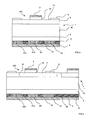
- a typical example for applying the invention is in a Reverse Conducting semiconductor device, also called Reverse Conducting insulated gate bipolar transistor (RC-IGBT) for soft turn-off performance as shown in figure 1 and 2 in both transistor mode and diode mode respectively.
- RC-IGBT Reverse Conducting insulated gate bipolar transistor
- the concept can also be applied easily in normal insulated gate bipolar transistors (IGBTs) and gate commutated transistors (GCTs).
- IGBTs insulated gate bipolar transistors
- GCTs gate commutated transistors
- the P+ regions dimensions are wider relative to the alternating N+ regions on the same plane to ensure good bipolar action under normal conditions.
- a bipolar punch-through semiconductor device comprises a semiconductor substrate 1, also called semiconductor wafer, with a first main side 11 and a second main side 12, which is arranged opposite of the first main side 11.
- a first electrical contact 2 is arranged on the first main side 11, and a second electrical contact 3 is arranged on the second main side 12.
- the device has at least a two-layer structure with layers of a first and a second conductivity type, one of the layers being a base layer 10 of the first conductivity type.
- a buffer layer 4 of the first conductivity type which has a higher doping concentration than the base layer 10, is arranged on the base layer 10 on the second main side 12.
- a first layer 5 is arranged in the substrate 1 between the buffer layer 4 and the second electrical contact 12, the first layer 5 comprising alternately at least one first region 51, 51' of the first conductivity type and at least one second region 52, 52' of the second conductivity type.
- the second region 52, 52' is an activated region, which has a depth of at maximum 2 ⁇ m and which second region has a junction profile 53, which drops 54 from 90 % to 10 % of the maximum doping concentration within at most 1 ⁇ m in depth direction, i.e. between the second region 52 and the buffer layer 4, as visualized in FIG 7 .
- the first region 51, 51' is a region, which has a depth of at maximum 2 ⁇ m.
- the first and/or second regions 51, 51', 52, 52' can be designed in a regular geometrical shape like in cells or stripes.
- the cells can have any shape like a square, rectangular or a circle or any other regular or irregular shape.
- the buffer layer 4 has a doping concentration of at maximum 5*10 16 cm -3 .
- inventive bipolar punch-through semiconductor devices are typically bipolar switched, reverse conducting switches or diodes.
- inventive bipolar punch-through semiconductor devices can for example be used in a converter.
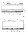
- FIG 8 such an inventive bipolar punch-through semiconductor device in form of a bipolar diode 101 is shown.
- the diode 101 comprises a base layer 10 of a first conductivity type, i.e. of n type, with a first main side 11 and a second main side 12 opposite the first main side 11.
- a second p doped layer 6 is arranged on the first main side 11.
- a first electrical contact 2, typically in form of a metal layer, is arranged on top of the second layer 6, i.e. on that side of the second layer 6, which lies opposite the base layer 10.
- first (n+) doped regions 51' with a higher doping concentration than the base layer 10 and a plurality of second (p+) doped regions 52', both of which regions are arranged alternately.
- a second electrical contact 3, typically in form of a metal layer is arranged on top of the first and second regions, i.e. on that side of the regions, which lies opposite the base layer 10.
- An (n+) doped buffer layer 4 is arranged between the base layer 10 and the first and second regions 51', 52'. This buffer layer 4 has a higher doping concentration than the base layer 10 and a lower doping concentration than the first regions 51'.
- the total area of the all second (p+) doped regions 52' in the diode is between 1 and 25 % of the total substrate area.
- the width of the first regions 51' is typically at least 50 ⁇ m, whereas the width of the second regions 52' is at least 5 ⁇ m.
- the doping concentration of the buffer layer 4 is at maximum 5*10 16 /cm 3 .
- the inventive bipolar punch-through semiconductor device can also be a bipolar switch, e.g. in form of a punch-through insulated gate bipolar transistor 100 as shown in FIG 1 .
- the insulated gate bipolar transistor 100 comprises an n type base layer 10 with a first main side 11 in form of an emitter side and a second main side 12 in form of a collector side opposite the emitter side.
- a p type second layer 6 is arranged on the emitter side.
- At least one n type source region 7 is arranged on the emitter side and is surrounded by the second layer 6.
- the at least one source region 7 has a higher doping than the base layer 10.
- An electrically insulating layer 8 is arranged on the emitter side on top of the base layer 10, the second layer 6 and the source region 7.
- An electrically conductive gate electrode 9 is arranged on the emitter side electrically insulated from the at least one second layer 6, the source regions 7 and the base layer 10 by the electrically insulating layer 8.
- the gate electrode 9 is embedded in the electrically insulating layer 8.
- the electrically insulating layer 8 comprises a first electrically insulating region 81, preferably made of a silicon dioxide, and a second electrically insulating region 82, preferably also made of a silicon dioxide, preferably of the same material as the first electrically insulating region 81.
- the second electrically insulating region 82 covers the first electrically insulating region 81.
- the first electrically insulating region 81 is arranged on top of the emitter side.
- the gate electrode 9 is embedded, typically it is completely embedded.
- the gate electrode 9 is typically made of a heavily doped polysilicon or a metal like aluminum.
- the at least one source region 7, the gate electrode 9 and the electrically insulating layer 8 are formed in such a way that an opening is created above the second layer 6. The opening is surrounded by the at least one source region 7, the gate electrode 9 and the electrically insulating layer 8.
- a first electrical contact 2 is arranged on the emitter side within the opening so that it is in direct electrical contact to the second layer 6 and the source regions 7.
- This first electrical contact 2 typically also covers the electrically insulating layer 8, but is separated and thus electrically insulated from the gate electrode 9 by the second electrically insulating region 82.
- the inventive IGBT may comprise a gate electrode, formed as trench gate electrode 9' as shown in FIG 2 .
- the trench gate electrode 9' is arranged in the same plane as the second layer 6 and adjacent to the source regions 7, separated from each other by a first insulating region 81, which also separates the gate electrode 9 from the base layer 10.
- a second insulating region 82 is arranged on top of the gate electrode formed as a trench gate electrode 9', thus insulating the trench gate electrode 9' from the first electrical contact 2.
- the IGBT further comprises an n type buffer layer 4, which is arranged between the base layer 10 and the second electrical contact 3, which buffer layer 4 has a higher doping than the base layer 10 and a lower doping than the first region 51.
- the at least one first and second region 51, 52 are arranged on the collector side between the buffer layer 4 and the second main electrode 3.
- the insulated gate bipolar transistor acts as a reverse conducting semiconductor device (RC-IGBT).
- a diode is formed between the first electrical contact 2, which forms an anode electrode in the diode, the second layer 6, part of which forms an anode layer, the base layer 10, part of which forms a base layer in the diode, the buffer layer 4, the first region 51, which region forms a cathode layer, and the second electrical contact 3, which forms a cathode electrode.
- an insulating bipolar transistor is formed between the first electrical contact 2, which forms an emitter electrode in the IGBT, the source region 7, the second layer 6, part of which forms a channel region, the base layer 10, part of which forms a base region in the IGBT, the buffer layer 4, the second region 52, which forms a collector layer, and the second electrical contact 3, part of which forms a collector electrode.
- the inventive bipolar punch-through semiconductor device can also be a bipolar switch in form of a punch-through integrated gate commutated thyristor (IGCT) as shown in FIG 3 .
- IGCT punch-through integrated gate commutated thyristor
- the semiconductor substrate comprises a four-layer pnpn structure with layers of different conductivity types.
- the structure defines an inner structure of a gate-commutated thyristor, which can be turned-off via a gate electrode.
- the structure comprises the following layers:
- the gate electrode 9 is arranged on the cathode side of the substrate 1 and electrically contacts the second layer 6.
- the at least one first and second region 51, 52 are arranged on the collector side between the buffer layer 4 and the second electrical contact 3.
- the inventive bipolar punch-through semiconductor device can also be a reverse conducting punch-through integrated gate commutated thyristor as shown in the figures 4 to 6 .
- Such a device comprises within one common substrate 1 an integrated gate commutated thyristor and adjacent to it, a freewheeling diode.
- the IGCT can comprise alternatingly first and second regions 51, 52, the second regions 52 preferably having a total area of 75 to 99 % of the total wafer area ( FIG 4 ) and the diode comprises a single n doped third region 55.
- the diode can comprise alternatingly first and second regions 51', 52', the second regions 52' preferably having a total area of 1 to 25 % of the total wafer area ( FIG 5 ).
- the IGCT comprises a single p doped fourth region 56.
- the first layer comprises the single third region 55 or the single fourth region 56, respectively.
- both the IGCT and the diode comprise alternatingly first and second regions 51, 52, 51', 52' according to the rules given above for the IGCT and the diode, respectively ( FIG 6 ).
- the layers on the first main side 11 are manufactured, resulting in a semi-fabricated semiconductor device.
- the layers on the second side 12 of the substrate 1 are manufactured after manufacturing the layers on the first side 11 either before or after creating the first electrical contact 2 or at any stage during the manufacturing of the layers on the second main side 12.
- the buffer layer is typically manufactured before the first and second regions are created.
- a semiconductor substrate 1 is provided with a first main side 11 and a second main side 12 opposite of the first main side 11.
- the finalized semiconductor device comprises at least a two-layer structure with layers of a first and a second conductivity type, one of the layers being a base layer 10 of the first conductivity type.
- a first electrical contact 2 is arranged on the first main side 11 and a second electrical contact 3 is arranged on the second main side 12.
- a buffer layer 4 of the first conductivity type is arranged on the base layer 10 on the second main side 12, which buffer layer 4 has a higher doping concentration than the base layer 10.
- a first layer 5 is arranged in the substrate 1 between the buffer layer 4 and the second electrical contact 3, the first layer 5 comprising alternately at least one first region 51, 51' of the first conductivity type and at least one second region 52, 52' of the second conductivity type.
- the manufacturing method for the creation of the first layer 5 comprises the following steps: For the creation of the first region 51, 51' particles of the first conductivity type are applied, in particular by implantation or deposition, on the second main side 12. For the creation of the second region 52, 52' particles of the second conductivity type are applied also preferably by implantation or deposition on the second main side 12. At least one of the steps of applying of particles of the first conductivity type or applying of particles of the second conductivity type is performed through a mask. The particles of the second conductivity type are afterwards activated at such conditions that the particles diffuse into the substrate 1 by not more than 2 ⁇ m and that the junction profile of the second region drops from 90 % to 10 % of the maximum doping concentration within at most 1 ⁇ m.
- the particles of the first conductivity type are activated at such conditions that the particles diffuse into the substrate 1 by not more than 2 ⁇ m.
- the particles for the creation of the first region 51, 51' or the second region 52, 52' or both regions 51, 51', 52, 52' are implanted or deposited.
- the doping concentration for the particles for the creation of the first region 51, 51' is 1 * 10 17 up to 1 * 10 20 cm -3
- the doping concentration for the particles for the creation of the second region 52, 52' is 1 * 10 16 up to 1 * 10 18 cm -3 .
- the total areas of the first and second regions are varied, in particular accordingly to the values given above for the varies semiconductor types.
- the particles for the creation of the first region 51, 51' or the second region 52, 52' or both regions 51, 51', 52, 52' can be activated by laser annealing or by a heat treatment.
- the heat treatment is performed at a temperature between 400 °C and 1000 °C and/or for at most 60 min.
- the particles for the creation of the first region 51, 51' and the second region 52, 52' can be activated simultaneously or alternatively, the particles can be activated consecutively for one layer after the other.
- the particles for the creation of the second region are Boron particles, as Boron particles have high activation energy with no or minimum diffusion occurring.
- a second electrical contact 3 is created on the second main side 12 on the first and second regions 51, 51', 52, 52' and if applicable the third or fourth region 55, 56 so that the second electrical contact 3 is in direct electrical contact to the first and second regions 51, 51', 52, 52' (and if applicable the third or fourth region 55, 56).
- metal is deposited on the second main side 12 for creating the second electrical contact 3.
Landscapes
- Electrodes Of Semiconductors (AREA)
- Bipolar Transistors (AREA)
- Thyristors (AREA)
Claims (11)
- Bipolarer Punch-Through-Halbleiterschalter mit einem Halbleitersubstrat (1), das mindestens eine Zwei-Schicht-Struktur mit Schichten eines ersten und eines zweiten Leitfähigkeitstyps umfasst, wobei eine der Schichten eine Basisschicht (10) des ersten Leitfähigkeitstyps ist,- wobei das Substrat eine erste Hauptseite (11) und eine zweite Hauptseite (12) umfasst,- wobei die erste Hauptseite (11) gegenüber der zweiten Hauptseite (12) angeordnet ist,- wobei ein erster elektrischer Kontakt (2) auf der ersten Hauptseite (11) angeordnet ist,- wobei ein zweiter elektrischer Kontakt (3) auf der zweiten Hauptseite (12) angeordnet ist,- wobei eine Pufferschicht (4) des ersten Leitfähigkeitstyps auf der Basisschicht (10) auf der zweiten Hauptseite (12) angeordnet ist, wobei die Pufferschicht (4) eine höhere Dotierungskonzentration als die Basisschicht (10) aufweist,- wobei eine erste Schicht (5) in dem Substrat (1) zwischen der Pufferschicht (4) und dem zweiten elektrischen Kontakt (3) angeordnet ist, wobei die erste Schicht (5) alternativ mindestens eine erste Region (51, 51') des ersten Leitfähigkeitstyps und mindestens eine zweite Region (52, 52') des zweiten Leitfähigkeitstyps umfasst,- wobei die zweite Region (52, 52') eine aktivierte Region ist, die eine Tiefe von maximal 2 µm aufweist,dadurch gekennzeichnet, dass die zweite Region (52, 52') ein Profil der Dotierungskonzentration aufweist, die innerhalb einer Distanz (54) zwischen 90 % bis 10 % der maximalen Dotierungskonzentration abfällt, wobei die Distanz (54) höchstens 1 µm beträgt, und dadurch, dass
mindestens eine der folgenden geometrischen Regeln erfüllt wird:- die Breite der zweiten Region (52, 52') beträgt mindestens 50 µm,- die Breite der ersten Region (51, 51') beträgt mindestens 5 µm,- der bipolare Schalter ist ein kommutierter Thyristor mit isoliertem Gate (102) und die gesamte Fläche der zweiten Regionen (52, 52') liegt zwischen 75 und 99 % der gesamten Substratfläche, oder- der bipolare Schalter ist ein bipolarer Transistor mit isoliertem Gate (100) und die gesamte Fläche der zweiten Regionen (52, 52') liegt zwischen 90 und 99 % der gesamten Waferfläche. - Bipolarer Punch-Through-Halbleiterschalter nach Anspruch 1, dadurch gekennzeichnet, dass
die erste Region (51, 51') eine Region ist, die eine Tiefe von maximal 2 µm aufweist. - Bipolarer Punch-Through-Halbleiterschalter nach Anspruch 1, dadurch gekennzeichnet, dass
die ersten und/oder zweiten Regionen (51, 51', 52, 52') in einer regelmäßigen geometrischen Form, in besonderen Zellen oder Streifen vorgesehen sind. - Bipolarer Punch-Through-Halbleiterschalter nach einem der Ansprüche 1 bis 3, dadurch gekennzeichnet, dass
die Pufferschicht (4) eine Dotierungskonzentration von höchstens 5 * 1018 cm-3 aufweist. - Bipolarer Punch-Through-Halbleiterschalter, die ein in Sperrrichtung leitender Halbleiterschalter ist, umfassend einen bipolaren Schalter in der Form eines kommutierten Thyristors mit isoliertem Gate (102) und eine Diode (101) auf einem gemeinsamen Substrat (1), wobei
der kommutierte Thyristor mit isoliertem Gate (102) gemäß einem der Ansprüche 1 bis 4 vorgesehen ist. - Bipolarer Punch-Through-Halbleiterschalter, dadurch gekennzeichnet, dass der Halbleiterschalter ein in Sperrrichtung leitender Halbleiterschalter ist, umfassend einen bipolaren Transistor mit isoliertem Gate nach einem der Ansprüche 1 bis 4 und eine Diode auf einem gemeinsamen Substrat (1), wobei die gesamte Fläche der zweiten Regionen (52, 52') 70 bis 90 % der gesamten Substratfläche beträgt.
- Verfahren zur Herstellung einer bipolaren Punch-Through-Halbleiterschalter nach einem der Ansprüche 1 bis 6 mit einem Halbleitersubstrat (1), das mindestens eine Zwei-Schicht-Struktur mit Schichten eines ersten und eines zweiten Leitfähigkeitstyps umfasst, wobei eine der Schichten eine Basisschicht (10) des ersten Leitfähigkeitstyps ist,- wobei das Substrat (1) eine erste Hauptseite (11) und eine zweite Hauptseite (12) umfasst,- wobei die erste Hauptseite (11) gegenüber der zweiten Hauptseite (12) angeordnet ist,- wobei ein erster elektrischer Kontakt (2) auf der ersten Hauptseite (11) angeordnet ist,- wobei ein zweiter elektrischer Kontakt (3) auf der zweiten Hauptseite (12) angeordnet ist,- wobei eine Pufferschicht (4) des ersten Leitfähigkeitstyps auf der Basisschicht (10) auf der zweiten Hauptseite (12) angeordnet ist, wobei die Pufferschicht (4) eine höhere Dotierungskonzentration als die Basisschicht (10) aufweist,wobei eine erste Schicht (5) in dem Substrat (1) zwischen der Pufferschicht (4) und dem zweiten elektrischen Kontakt (3) angeordnet ist, wobei die erste Schicht (5) alternativ mindestens eine erste Region (51, 51') des ersten Leitfähigkeitstyps und mindestens eine zweite Region (52, 52') des zweiten Leitfähigkeitstyps umfasst,
wobei das Herstellungsverfahren die folgenden Schritte umfasst:das Substrat (1) wird bereitgestellt, indemzur Erzeugung der ersten Schicht (5) die folgenden Schritte durchgeführt werden:- zur Erzeugung der ersten Region (51, 51') werden Partikel des ersten Leitfähigkeitstyps auf die zweite Hauptseite (12) aufgebracht,- zur Erzeugung der zweiten Region (52, 52') werden Partikel des zweiten Leitfähigkeitstyps auf die zweite Hauptseite (12) aufgebracht,- die Partikel des zweiten Leitfähigkeitstyps werden anschließend bei derartigen Bedingungen aktiviert, dass die Partikel um nicht mehr als 2 µm in das Substrat (1) diffundieren und dass das Profil der Dotierungskonzentration der zweiten Region (52, 52') innerhalb einer Distanz (54) zwischen 90 % und 10 % der maximalen Dotierungskonzentration abfällt, wobei die Distanz (54) höchsten 1 µm beträgt,- mindestens einer der Schritte des Aufbringens von Partikeln zur Erzeugung der ersten Region (51, 51') oder der zweiten Region (52) wird durch eine Maske durchgeführt. - Verfahren nach Anspruch 7, dadurch gekennzeichnet, dass- die Partikel des ersten Leitfähigkeitstyps bei derartigen Bedingungen aktiviert werden, dass die Partikel um nicht mehr als 2 µm in das Substrat (1) diffundieren.
- Verfahren nach einem der Ansprüche 7 oder 8, dadurch gekennzeichnet, dass mindestens eine der folgenden geometrischen Regeln erfüllt wird:- die erste Region (51, 51') wird derart erzeugt, dass das Profil der Dotierungskonzentration der ersten Region (51, 51') innerhalb einer Distanz (54) zwischen 90 % und 10 % der maximalen Dotierungskonzentration abfällt, wobei die Distanz (54) maximal 1 µm beträgt,- die Tiefe der ersten Region (51) ist gleich oder größer als die Tiefe der zweiten Region (52, 52').
- Verfahren nach einem der Ansprüche 7 bis 9, dadurch gekennzeichnet, dass die Partikel zur Erzeugung mindestens einer der Regionen, wobei die Regionen die erste Region und die zweite Region (51, 51', 52, 52') sind, mit einer Dotierungskonzentration von 1 * 1017 bis zu 1 * 1020 cm-3 für die Partikel zur Erzeugung der ersten Region (51, 51') und/oder 1 * 1016 bis zu 1 * 1018 cm-3 für die Partikel zur Erzeugung der zweiten Region (52, 52') aufgebracht werden.
- Verfahren nach einem der Ansprüche 7 bis 10, dadurch gekennzeichnet, dass die Partikel zur Erzeugung mindestens einer der Regionen, wobei die Regionen die erste Region und die zweite Region (51, 51', 52, 52') sind, aktiviert werden- durch Laser-Glühen oder- durch eine Wärmebehandlung bei einer Temperatur zwischen 400 °C und 1000 °C,- durch eine Wärmebehandlung über höchsten 60 Min.,wobei die Partikel zur Erzeugung der ersten Region (51, 51') und der zweiten Region (52, 52') gleichzeitig oder nacheinander aktiviert werden.
Priority Applications (1)
| Application Number | Priority Date | Filing Date | Title |
|---|---|---|---|
| EP09779699.9A EP2359404B1 (de) | 2008-12-15 | 2009-06-10 | Bipolar-punch-through-halbleiteranordnung und verfahren zur herstellung einer solchen halbleiteranordnung |
Applications Claiming Priority (3)
| Application Number | Priority Date | Filing Date | Title |
|---|---|---|---|
| EP08171605 | 2008-12-15 | ||
| PCT/EP2009/057149 WO2010069618A1 (en) | 2008-12-15 | 2009-06-10 | Bipolar punch-through semiconductor device and method for manufacturing such a semiconductor device |
| EP09779699.9A EP2359404B1 (de) | 2008-12-15 | 2009-06-10 | Bipolar-punch-through-halbleiteranordnung und verfahren zur herstellung einer solchen halbleiteranordnung |
Publications (2)
| Publication Number | Publication Date |
|---|---|
| EP2359404A1 EP2359404A1 (de) | 2011-08-24 |
| EP2359404B1 true EP2359404B1 (de) | 2015-01-14 |
Family
ID=41016979
Family Applications (1)
| Application Number | Title | Priority Date | Filing Date |
|---|---|---|---|
| EP09779699.9A Active EP2359404B1 (de) | 2008-12-15 | 2009-06-10 | Bipolar-punch-through-halbleiteranordnung und verfahren zur herstellung einer solchen halbleiteranordnung |
Country Status (6)
| Country | Link |
|---|---|
| US (1) | US8508016B2 (de) |
| EP (1) | EP2359404B1 (de) |
| JP (1) | JP2012512538A (de) |
| KR (1) | KR20110094066A (de) |
| CN (1) | CN102318071B (de) |
| WO (1) | WO2010069618A1 (de) |
Families Citing this family (14)
| Publication number | Priority date | Publication date | Assignee | Title |
|---|---|---|---|---|
| EP2535940B1 (de) * | 2011-06-14 | 2013-08-21 | ABB Technology AG | Bipolare Diode und Verfahren zur deren Herstellung |
| CN103311270B (zh) * | 2012-03-12 | 2015-10-14 | 上海华虹宏力半导体制造有限公司 | 逆导型igbt半导体器件及制造方法 |
| US9018674B2 (en) * | 2012-04-06 | 2015-04-28 | Infineon Technologies Ag | Reverse conducting insulated gate bipolar transistor |
| CN102832240A (zh) * | 2012-09-11 | 2012-12-19 | 电子科技大学 | 一种集电极终端具有介质层的绝缘栅双极型晶体管 |
| KR101398125B1 (ko) * | 2013-06-19 | 2014-05-27 | 주식회사 시지트로닉스 | 자기정렬 고속 회복 다이오드 및 그 제조 방법 |
| DE102016117723A1 (de) | 2016-09-20 | 2018-03-22 | Infineon Technologies Ag | Diodenstruktur eines Leistungshalbleiterbauelements |
| CN106847810A (zh) * | 2016-12-27 | 2017-06-13 | 湖南大学 | Bjt辅助的改进型gto结构、控制方法及制备方法 |
| CN108122971B (zh) * | 2017-12-25 | 2020-11-27 | 电子科技大学 | 一种rc-igbt器件及其制备方法 |
| WO2020240728A1 (ja) | 2019-05-29 | 2020-12-03 | 三菱電機株式会社 | 半導体装置、および、半導体装置の製造方法 |
| GB2589057B (en) | 2019-08-27 | 2023-07-19 | Mqsemi Ag | Bipolar semiconductor device and method for manufacturing such a semiconductor device |
| GB2589543A (en) | 2019-09-09 | 2021-06-09 | Mqsemi Ag | Method for forming a low injection P-type contact region and power semiconductor devices with the same |
| CN110797403B (zh) * | 2019-10-18 | 2023-08-01 | 上海睿驱微电子科技有限公司 | 一种rc-igbt半导体装置 |
| EP3935671B1 (de) * | 2020-03-17 | 2022-05-11 | Hitachi Energy Switzerland AG | Halbleiterbauelement mit schrittweiser injektion von ladungsträgern für eine weichere reverse-recovery |
| KR102372374B1 (ko) * | 2020-09-11 | 2022-03-11 | (주) 트리노테크놀로지 | 고속 및 소프트 회복 특성을 가진 하이브리드 다이오드 |
Family Cites Families (11)
| Publication number | Priority date | Publication date | Assignee | Title |
|---|---|---|---|---|
| JPH07109882B2 (ja) * | 1988-02-26 | 1995-11-22 | 三菱電機株式会社 | バイポーラ型半導体スイッチング装置 |
| JPH0242447U (de) * | 1988-09-19 | 1990-03-23 | ||
| JP2504609B2 (ja) * | 1990-07-10 | 1996-06-05 | 株式会社東芝 | 半導体装置 |
| JPH05347413A (ja) | 1992-06-12 | 1993-12-27 | Toshiba Corp | 半導体装置の製造方法 |
| JP2851027B2 (ja) * | 1993-10-21 | 1999-01-27 | 東洋電機製造株式会社 | バッファを有する半導体スイッチング素子 |
| JPH07153942A (ja) * | 1993-12-01 | 1995-06-16 | Matsushita Electron Corp | 絶縁ゲート型バイポーラトランジスタおよびその製造方法 |
| DE4431294A1 (de) * | 1994-09-02 | 1996-03-07 | Abb Management Ag | Abschaltbarer Thyristor für hohe Blockierspannungen und kleiner Bauelementdicke |
| JP2005057235A (ja) * | 2003-07-24 | 2005-03-03 | Mitsubishi Electric Corp | 絶縁ゲート型バイポーラトランジスタ及びその製造方法、並びに、インバータ回路 |
| JP4899405B2 (ja) * | 2004-11-08 | 2012-03-21 | 株式会社デンソー | 炭化珪素半導体装置およびその製造方法 |
| DE102005035648B4 (de) * | 2005-07-29 | 2010-06-10 | Infineon Technologies Austria Ag | Verfahren zur Herstellung eines Hochleistungsbauelements |
| JP5283326B2 (ja) * | 2006-10-27 | 2013-09-04 | 三菱電機株式会社 | 半導体装置およびその製造方法 |
-
2009
- 2009-06-10 WO PCT/EP2009/057149 patent/WO2010069618A1/en not_active Ceased
- 2009-06-10 KR KR1020117013653A patent/KR20110094066A/ko not_active Ceased
- 2009-06-10 EP EP09779699.9A patent/EP2359404B1/de active Active
- 2009-06-10 JP JP2011541239A patent/JP2012512538A/ja active Pending
- 2009-06-10 CN CN200980157041.9A patent/CN102318071B/zh active Active
-
2011
- 2011-06-15 US US13/160,945 patent/US8508016B2/en active Active
Also Published As
| Publication number | Publication date |
|---|---|
| US20110278694A1 (en) | 2011-11-17 |
| CN102318071B (zh) | 2015-08-19 |
| KR20110094066A (ko) | 2011-08-19 |
| EP2359404A1 (de) | 2011-08-24 |
| WO2010069618A1 (en) | 2010-06-24 |
| CN102318071A (zh) | 2012-01-11 |
| US8508016B2 (en) | 2013-08-13 |
| JP2012512538A (ja) | 2012-05-31 |
Similar Documents
| Publication | Publication Date | Title |
|---|---|---|
| US8508016B2 (en) | Bipolar punch-through semiconductor device and method for manufacturing such a semiconductor device | |
| JP4791704B2 (ja) | 逆導通型半導体素子とその製造方法 | |
| US7932583B2 (en) | Reduced free-charge carrier lifetime device | |
| US6051850A (en) | Insulated gate bipolar junction transistors having built-in freewheeling diodes therein | |
| EP2223340B1 (de) | Rückwärtsleitendes halbleiterbauelement und verfahren zur herstellung eines solchen rückwärtsleitenden halbleiterbauelements | |
| US11699744B2 (en) | Semiconductor device and semiconductor apparatus | |
| EP2341528A1 (de) | Leistungshalbleiterbauelement und Verfahren zu dessen Herstellung | |
| US7816706B2 (en) | Power semiconductor device | |
| JP2014086600A (ja) | 半導体装置、半導体装置の製造方法および半導体装置の制御方法 | |
| EP3948956B1 (de) | Segmentierte leistungsdiodenstruktur mit verbesserter reverse recovery | |
| KR101452098B1 (ko) | 전력 반도체 소자 및 그 제조 방법 | |
| JP7171527B2 (ja) | 半導体装置および電力変換装置 | |
| JP2000150859A (ja) | ダイオード | |
| US6621120B2 (en) | Semiconductor device | |
| JP5135666B2 (ja) | 電力変換装置 | |
| US20100301384A1 (en) | Diode | |
| WO2010142342A1 (en) | Power semiconductor device | |
| KR20150031668A (ko) | 전력 반도체 소자 | |
| KR101928395B1 (ko) | 전력 반도체 소자 및 그 제조 방법 | |
| JP2025127183A (ja) | 半導体装置および電力変換装置 | |
| JP2009158643A (ja) | 半導体装置 |
Legal Events
| Date | Code | Title | Description |
|---|---|---|---|
| PUAI | Public reference made under article 153(3) epc to a published international application that has entered the european phase |
Free format text: ORIGINAL CODE: 0009012 |
|
| 17P | Request for examination filed |
Effective date: 20110610 |
|
| AK | Designated contracting states |
Kind code of ref document: A1 Designated state(s): AT BE BG CH CY CZ DE DK EE ES FI FR GB GR HR HU IE IS IT LI LT LU LV MC MK MT NL NO PL PT RO SE SI SK TR |
|
| RIN1 | Information on inventor provided before grant (corrected) |
Inventor name: RAHIMO, MUNAF Inventor name: KOPTA, ARNOST Inventor name: SCHLAPBACH, ULRICH |
|
| RIN1 | Information on inventor provided before grant (corrected) |
Inventor name: SCHLAPBACH, ULRICH Inventor name: KOPTA, ARNOST Inventor name: RAHIMO, MUNAF |
|
| DAX | Request for extension of the european patent (deleted) | ||
| 17Q | First examination report despatched |
Effective date: 20130807 |
|
| GRAP | Despatch of communication of intention to grant a patent |
Free format text: ORIGINAL CODE: EPIDOSNIGR1 |
|
| INTG | Intention to grant announced |
Effective date: 20140828 |
|
| GRAS | Grant fee paid |
Free format text: ORIGINAL CODE: EPIDOSNIGR3 |
|
| GRAA | (expected) grant |
Free format text: ORIGINAL CODE: 0009210 |
|
| AK | Designated contracting states |
Kind code of ref document: B1 Designated state(s): AT BE BG CH CY CZ DE DK EE ES FI FR GB GR HR HU IE IS IT LI LT LU LV MC MK MT NL NO PL PT RO SE SI SK TR |
|
| REG | Reference to a national code |
Ref country code: GB Ref legal event code: FG4D |
|
| REG | Reference to a national code |
Ref country code: CH Ref legal event code: EP |
|
| REG | Reference to a national code |
Ref country code: IE Ref legal event code: FG4D |
|
| REG | Reference to a national code |
Ref country code: AT Ref legal event code: REF Ref document number: 707430 Country of ref document: AT Kind code of ref document: T Effective date: 20150215 |
|
| REG | Reference to a national code |
Ref country code: DE Ref legal event code: R096 Ref document number: 602009028998 Country of ref document: DE Effective date: 20150226 |
|
| REG | Reference to a national code |
Ref country code: NL Ref legal event code: VDEP Effective date: 20150114 |
|
| REG | Reference to a national code |
Ref country code: AT Ref legal event code: MK05 Ref document number: 707430 Country of ref document: AT Kind code of ref document: T Effective date: 20150114 |
|
| REG | Reference to a national code |
Ref country code: LT Ref legal event code: MG4D |
|
| PG25 | Lapsed in a contracting state [announced via postgrant information from national office to epo] |
Ref country code: BG Free format text: LAPSE BECAUSE OF FAILURE TO SUBMIT A TRANSLATION OF THE DESCRIPTION OR TO PAY THE FEE WITHIN THE PRESCRIBED TIME-LIMIT Effective date: 20150414 Ref country code: ES Free format text: LAPSE BECAUSE OF FAILURE TO SUBMIT A TRANSLATION OF THE DESCRIPTION OR TO PAY THE FEE WITHIN THE PRESCRIBED TIME-LIMIT Effective date: 20150114 Ref country code: NO Free format text: LAPSE BECAUSE OF FAILURE TO SUBMIT A TRANSLATION OF THE DESCRIPTION OR TO PAY THE FEE WITHIN THE PRESCRIBED TIME-LIMIT Effective date: 20150414 Ref country code: FI Free format text: LAPSE BECAUSE OF FAILURE TO SUBMIT A TRANSLATION OF THE DESCRIPTION OR TO PAY THE FEE WITHIN THE PRESCRIBED TIME-LIMIT Effective date: 20150114 Ref country code: LT Free format text: LAPSE BECAUSE OF FAILURE TO SUBMIT A TRANSLATION OF THE DESCRIPTION OR TO PAY THE FEE WITHIN THE PRESCRIBED TIME-LIMIT Effective date: 20150114 Ref country code: SE Free format text: LAPSE BECAUSE OF FAILURE TO SUBMIT A TRANSLATION OF THE DESCRIPTION OR TO PAY THE FEE WITHIN THE PRESCRIBED TIME-LIMIT Effective date: 20150114 Ref country code: HR Free format text: LAPSE BECAUSE OF FAILURE TO SUBMIT A TRANSLATION OF THE DESCRIPTION OR TO PAY THE FEE WITHIN THE PRESCRIBED TIME-LIMIT Effective date: 20150114 |
|
| PG25 | Lapsed in a contracting state [announced via postgrant information from national office to epo] |
Ref country code: PL Free format text: LAPSE BECAUSE OF FAILURE TO SUBMIT A TRANSLATION OF THE DESCRIPTION OR TO PAY THE FEE WITHIN THE PRESCRIBED TIME-LIMIT Effective date: 20150114 Ref country code: AT Free format text: LAPSE BECAUSE OF FAILURE TO SUBMIT A TRANSLATION OF THE DESCRIPTION OR TO PAY THE FEE WITHIN THE PRESCRIBED TIME-LIMIT Effective date: 20150114 Ref country code: NL Free format text: LAPSE BECAUSE OF FAILURE TO SUBMIT A TRANSLATION OF THE DESCRIPTION OR TO PAY THE FEE WITHIN THE PRESCRIBED TIME-LIMIT Effective date: 20150114 Ref country code: GR Free format text: LAPSE BECAUSE OF FAILURE TO SUBMIT A TRANSLATION OF THE DESCRIPTION OR TO PAY THE FEE WITHIN THE PRESCRIBED TIME-LIMIT Effective date: 20150415 Ref country code: IS Free format text: LAPSE BECAUSE OF FAILURE TO SUBMIT A TRANSLATION OF THE DESCRIPTION OR TO PAY THE FEE WITHIN THE PRESCRIBED TIME-LIMIT Effective date: 20150514 Ref country code: LV Free format text: LAPSE BECAUSE OF FAILURE TO SUBMIT A TRANSLATION OF THE DESCRIPTION OR TO PAY THE FEE WITHIN THE PRESCRIBED TIME-LIMIT Effective date: 20150114 |
|
| REG | Reference to a national code |
Ref country code: DE Ref legal event code: R097 Ref document number: 602009028998 Country of ref document: DE |
|
| PG25 | Lapsed in a contracting state [announced via postgrant information from national office to epo] |
Ref country code: SK Free format text: LAPSE BECAUSE OF FAILURE TO SUBMIT A TRANSLATION OF THE DESCRIPTION OR TO PAY THE FEE WITHIN THE PRESCRIBED TIME-LIMIT Effective date: 20150114 Ref country code: RO Free format text: LAPSE BECAUSE OF FAILURE TO SUBMIT A TRANSLATION OF THE DESCRIPTION OR TO PAY THE FEE WITHIN THE PRESCRIBED TIME-LIMIT Effective date: 20150114 Ref country code: DK Free format text: LAPSE BECAUSE OF FAILURE TO SUBMIT A TRANSLATION OF THE DESCRIPTION OR TO PAY THE FEE WITHIN THE PRESCRIBED TIME-LIMIT Effective date: 20150114 Ref country code: CZ Free format text: LAPSE BECAUSE OF FAILURE TO SUBMIT A TRANSLATION OF THE DESCRIPTION OR TO PAY THE FEE WITHIN THE PRESCRIBED TIME-LIMIT Effective date: 20150114 Ref country code: EE Free format text: LAPSE BECAUSE OF FAILURE TO SUBMIT A TRANSLATION OF THE DESCRIPTION OR TO PAY THE FEE WITHIN THE PRESCRIBED TIME-LIMIT Effective date: 20150114 |
|
| PLBE | No opposition filed within time limit |
Free format text: ORIGINAL CODE: 0009261 |
|
| STAA | Information on the status of an ep patent application or granted ep patent |
Free format text: STATUS: NO OPPOSITION FILED WITHIN TIME LIMIT |
|
| 26N | No opposition filed |
Effective date: 20151015 |
|
| PG25 | Lapsed in a contracting state [announced via postgrant information from national office to epo] |
Ref country code: IT Free format text: LAPSE BECAUSE OF FAILURE TO SUBMIT A TRANSLATION OF THE DESCRIPTION OR TO PAY THE FEE WITHIN THE PRESCRIBED TIME-LIMIT Effective date: 20150114 |
|
| PG25 | Lapsed in a contracting state [announced via postgrant information from national office to epo] |
Ref country code: MC Free format text: LAPSE BECAUSE OF FAILURE TO SUBMIT A TRANSLATION OF THE DESCRIPTION OR TO PAY THE FEE WITHIN THE PRESCRIBED TIME-LIMIT Effective date: 20150114 |
|
| REG | Reference to a national code |
Ref country code: CH Ref legal event code: PL |
|
| PG25 | Lapsed in a contracting state [announced via postgrant information from national office to epo] |
Ref country code: SI Free format text: LAPSE BECAUSE OF FAILURE TO SUBMIT A TRANSLATION OF THE DESCRIPTION OR TO PAY THE FEE WITHIN THE PRESCRIBED TIME-LIMIT Effective date: 20150114 Ref country code: LU Free format text: LAPSE BECAUSE OF FAILURE TO SUBMIT A TRANSLATION OF THE DESCRIPTION OR TO PAY THE FEE WITHIN THE PRESCRIBED TIME-LIMIT Effective date: 20150610 |
|
| REG | Reference to a national code |
Ref country code: IE Ref legal event code: MM4A |
|
| REG | Reference to a national code |
Ref country code: FR Ref legal event code: ST Effective date: 20160229 |
|
| PG25 | Lapsed in a contracting state [announced via postgrant information from national office to epo] |
Ref country code: LI Free format text: LAPSE BECAUSE OF NON-PAYMENT OF DUE FEES Effective date: 20150630 Ref country code: IE Free format text: LAPSE BECAUSE OF NON-PAYMENT OF DUE FEES Effective date: 20150610 Ref country code: CH Free format text: LAPSE BECAUSE OF NON-PAYMENT OF DUE FEES Effective date: 20150630 |
|
| PG25 | Lapsed in a contracting state [announced via postgrant information from national office to epo] |
Ref country code: BE Free format text: LAPSE BECAUSE OF FAILURE TO SUBMIT A TRANSLATION OF THE DESCRIPTION OR TO PAY THE FEE WITHIN THE PRESCRIBED TIME-LIMIT Effective date: 20150114 Ref country code: FR Free format text: LAPSE BECAUSE OF NON-PAYMENT OF DUE FEES Effective date: 20150630 |
|
| PG25 | Lapsed in a contracting state [announced via postgrant information from national office to epo] |
Ref country code: MT Free format text: LAPSE BECAUSE OF FAILURE TO SUBMIT A TRANSLATION OF THE DESCRIPTION OR TO PAY THE FEE WITHIN THE PRESCRIBED TIME-LIMIT Effective date: 20150114 |
|
| REG | Reference to a national code |
Ref country code: DE Ref legal event code: R081 Ref document number: 602009028998 Country of ref document: DE Owner name: HITACHI ENERGY SWITZERLAND AG, CH Free format text: FORMER OWNER: ABB TECHNOLOGY AG, ZUERICH, CH Ref country code: DE Ref legal event code: R081 Ref document number: 602009028998 Country of ref document: DE Owner name: ABB SCHWEIZ AG, CH Free format text: FORMER OWNER: ABB TECHNOLOGY AG, ZUERICH, CH Ref country code: DE Ref legal event code: R081 Ref document number: 602009028998 Country of ref document: DE Owner name: ABB POWER GRIDS SWITZERLAND AG, CH Free format text: FORMER OWNER: ABB TECHNOLOGY AG, ZUERICH, CH Ref country code: DE Ref legal event code: R082 Ref document number: 602009028998 Country of ref document: DE Representative=s name: DENNEMEYER & ASSOCIATES S.A., DE Ref country code: DE Ref legal event code: R082 Ref document number: 602009028998 Country of ref document: DE Representative=s name: ZIMMERMANN & PARTNER PATENTANWAELTE MBB, DE |
|
| PG25 | Lapsed in a contracting state [announced via postgrant information from national office to epo] |
Ref country code: HU Free format text: LAPSE BECAUSE OF FAILURE TO SUBMIT A TRANSLATION OF THE DESCRIPTION OR TO PAY THE FEE WITHIN THE PRESCRIBED TIME-LIMIT; INVALID AB INITIO Effective date: 20090610 |
|
| PG25 | Lapsed in a contracting state [announced via postgrant information from national office to epo] |
Ref country code: CY Free format text: LAPSE BECAUSE OF FAILURE TO SUBMIT A TRANSLATION OF THE DESCRIPTION OR TO PAY THE FEE WITHIN THE PRESCRIBED TIME-LIMIT Effective date: 20150114 |
|
| PG25 | Lapsed in a contracting state [announced via postgrant information from national office to epo] |
Ref country code: TR Free format text: LAPSE BECAUSE OF FAILURE TO SUBMIT A TRANSLATION OF THE DESCRIPTION OR TO PAY THE FEE WITHIN THE PRESCRIBED TIME-LIMIT Effective date: 20150114 |
|
| REG | Reference to a national code |
Ref country code: GB Ref legal event code: 732E Free format text: REGISTERED BETWEEN 20180426 AND 20180502 |
|
| PG25 | Lapsed in a contracting state [announced via postgrant information from national office to epo] |
Ref country code: PT Free format text: LAPSE BECAUSE OF FAILURE TO SUBMIT A TRANSLATION OF THE DESCRIPTION OR TO PAY THE FEE WITHIN THE PRESCRIBED TIME-LIMIT Effective date: 20150114 Ref country code: MK Free format text: LAPSE BECAUSE OF FAILURE TO SUBMIT A TRANSLATION OF THE DESCRIPTION OR TO PAY THE FEE WITHIN THE PRESCRIBED TIME-LIMIT Effective date: 20150114 |
|
| REG | Reference to a national code |
Ref country code: DE Ref legal event code: R081 Ref document number: 602009028998 Country of ref document: DE Owner name: HITACHI ENERGY SWITZERLAND AG, CH Free format text: FORMER OWNER: ABB SCHWEIZ AG, BADEN, CH Ref country code: DE Ref legal event code: R082 Ref document number: 602009028998 Country of ref document: DE Representative=s name: DENNEMEYER & ASSOCIATES RECHTSANWALTSGESELLSCH, DE Ref country code: DE Ref legal event code: R081 Ref document number: 602009028998 Country of ref document: DE Owner name: HITACHI ENERGY LTD, CH Free format text: FORMER OWNER: ABB SCHWEIZ AG, BADEN, CH Ref country code: DE Ref legal event code: R082 Ref document number: 602009028998 Country of ref document: DE Representative=s name: DENNEMEYER & ASSOCIATES S.A., DE Ref country code: DE Ref legal event code: R081 Ref document number: 602009028998 Country of ref document: DE Owner name: ABB POWER GRIDS SWITZERLAND AG, CH Free format text: FORMER OWNER: ABB SCHWEIZ AG, BADEN, CH |
|
| REG | Reference to a national code |
Ref country code: GB Ref legal event code: 732E Free format text: REGISTERED BETWEEN 20210909 AND 20210915 |
|
| REG | Reference to a national code |
Ref country code: DE Ref legal event code: R081 Ref document number: 602009028998 Country of ref document: DE Owner name: HITACHI ENERGY SWITZERLAND AG, CH Free format text: FORMER OWNER: ABB POWER GRIDS SWITZERLAND AG, BADEN, CH Ref country code: DE Ref legal event code: R081 Ref document number: 602009028998 Country of ref document: DE Owner name: HITACHI ENERGY LTD, CH Free format text: FORMER OWNER: ABB POWER GRIDS SWITZERLAND AG, BADEN, CH |
|
| P01 | Opt-out of the competence of the unified patent court (upc) registered |
Effective date: 20230527 |
|
| REG | Reference to a national code |
Ref country code: DE Ref legal event code: R082 Ref document number: 602009028998 Country of ref document: DE Representative=s name: DENNEMEYER & ASSOCIATES RECHTSANWALTSGESELLSCH, DE Ref country code: DE Ref legal event code: R082 Ref document number: 602009028998 Country of ref document: DE Representative=s name: DENNEMEYER & ASSOCIATES S.A., DE Ref country code: DE Ref legal event code: R081 Ref document number: 602009028998 Country of ref document: DE Owner name: HITACHI ENERGY LTD, CH Free format text: FORMER OWNER: HITACHI ENERGY SWITZERLAND AG, BADEN, CH |
|
| REG | Reference to a national code |
Ref country code: GB Ref legal event code: 732E Free format text: REGISTERED BETWEEN 20240718 AND 20240724 |
|
| REG | Reference to a national code |
Ref country code: DE Ref legal event code: R079 Ref document number: 602009028998 Country of ref document: DE Free format text: PREVIOUS MAIN CLASS: H01L0029080000 Ipc: H10D0062130000 |
|
| REG | Reference to a national code |
Ref country code: DE Ref legal event code: R082 Ref document number: 602009028998 Country of ref document: DE Representative=s name: DENNEMEYER & ASSOCIATES RECHTSANWALTSGESELLSCH, DE |
|
| PGFP | Annual fee paid to national office [announced via postgrant information from national office to epo] |
Ref country code: DE Payment date: 20250618 Year of fee payment: 17 |
|
| PGFP | Annual fee paid to national office [announced via postgrant information from national office to epo] |
Ref country code: GB Payment date: 20250618 Year of fee payment: 17 |