EP2360742A2 - Procédé et supports pour cellule solaire haute puissance - Google Patents
Procédé et supports pour cellule solaire haute puissance Download PDFInfo
- Publication number
- EP2360742A2 EP2360742A2 EP11165416A EP11165416A EP2360742A2 EP 2360742 A2 EP2360742 A2 EP 2360742A2 EP 11165416 A EP11165416 A EP 11165416A EP 11165416 A EP11165416 A EP 11165416A EP 2360742 A2 EP2360742 A2 EP 2360742A2
- Authority
- EP
- European Patent Office
- Prior art keywords
- solar cell
- photons
- photon
- filter
- energies
- Prior art date
- Legal status (The legal status is an assumption and is not a legal conclusion. Google has not performed a legal analysis and makes no representation as to the accuracy of the status listed.)
- Withdrawn
Links
- 238000000034 method Methods 0.000 title claims abstract description 30
- 238000001228 spectrum Methods 0.000 description 20
- 239000000463 material Substances 0.000 description 16
- 229910052782 aluminium Inorganic materials 0.000 description 9
- XAGFODPZIPBFFR-UHFFFAOYSA-N aluminium Chemical compound [Al] XAGFODPZIPBFFR-UHFFFAOYSA-N 0.000 description 9
- 238000004519 manufacturing process Methods 0.000 description 9
- 239000012071 phase Substances 0.000 description 7
- 239000004065 semiconductor Substances 0.000 description 7
- 230000009102 absorption Effects 0.000 description 6
- 238000010521 absorption reaction Methods 0.000 description 6
- 239000011888 foil Substances 0.000 description 6
- 230000008569 process Effects 0.000 description 6
- JBRZTFJDHDCESZ-UHFFFAOYSA-N AsGa Chemical compound [As]#[Ga] JBRZTFJDHDCESZ-UHFFFAOYSA-N 0.000 description 5
- XUIMIQQOPSSXEZ-UHFFFAOYSA-N Silicon Chemical compound [Si] XUIMIQQOPSSXEZ-UHFFFAOYSA-N 0.000 description 5
- 238000010586 diagram Methods 0.000 description 5
- 230000005611 electricity Effects 0.000 description 5
- 230000003287 optical effect Effects 0.000 description 5
- 230000004044 response Effects 0.000 description 5
- 229910052710 silicon Inorganic materials 0.000 description 5
- 239000010703 silicon Substances 0.000 description 5
- 229910005540 GaP Inorganic materials 0.000 description 4
- GPXJNWSHGFTCBW-UHFFFAOYSA-N Indium phosphide Chemical compound [In]#P GPXJNWSHGFTCBW-UHFFFAOYSA-N 0.000 description 4
- 238000006243 chemical reaction Methods 0.000 description 4
- HZXMRANICFIONG-UHFFFAOYSA-N gallium phosphide Chemical compound [Ga]#P HZXMRANICFIONG-UHFFFAOYSA-N 0.000 description 4
- PCHJSUWPFVWCPO-UHFFFAOYSA-N gold Chemical compound [Au] PCHJSUWPFVWCPO-UHFFFAOYSA-N 0.000 description 4
- 229910052737 gold Inorganic materials 0.000 description 4
- 239000010931 gold Substances 0.000 description 4
- WPYVAWXEWQSOGY-UHFFFAOYSA-N indium antimonide Chemical compound [Sb]#[In] WPYVAWXEWQSOGY-UHFFFAOYSA-N 0.000 description 4
- 230000003993 interaction Effects 0.000 description 4
- 229910002601 GaN Inorganic materials 0.000 description 3
- 229910001218 Gallium arsenide Inorganic materials 0.000 description 3
- 239000004411 aluminium Substances 0.000 description 3
- 230000008901 benefit Effects 0.000 description 3
- 230000036755 cellular response Effects 0.000 description 3
- 238000000576 coating method Methods 0.000 description 3
- 238000005516 engineering process Methods 0.000 description 3
- 239000010408 film Substances 0.000 description 3
- 238000001914 filtration Methods 0.000 description 3
- 229910052738 indium Inorganic materials 0.000 description 3
- APFVFJFRJDLVQX-UHFFFAOYSA-N indium atom Chemical compound [In] APFVFJFRJDLVQX-UHFFFAOYSA-N 0.000 description 3
- 229910000530 Gallium indium arsenide Inorganic materials 0.000 description 2
- KTSFMFGEAAANTF-UHFFFAOYSA-N [Cu].[Se].[Se].[In] Chemical compound [Cu].[Se].[Se].[In] KTSFMFGEAAANTF-UHFFFAOYSA-N 0.000 description 2
- CJOBVZJTOIVNNF-UHFFFAOYSA-N cadmium sulfide Chemical compound [Cd]=S CJOBVZJTOIVNNF-UHFFFAOYSA-N 0.000 description 2
- 229910052980 cadmium sulfide Inorganic materials 0.000 description 2
- 238000002109 crystal growth method Methods 0.000 description 2
- 230000000694 effects Effects 0.000 description 2
- 238000001413 far-infrared spectroscopy Methods 0.000 description 2
- 230000004907 flux Effects 0.000 description 2
- 239000011521 glass Substances 0.000 description 2
- 238000004943 liquid phase epitaxy Methods 0.000 description 2
- 229910001635 magnesium fluoride Inorganic materials 0.000 description 2
- 229910052751 metal Inorganic materials 0.000 description 2
- 239000002184 metal Substances 0.000 description 2
- 229910021420 polycrystalline silicon Inorganic materials 0.000 description 2
- 230000035945 sensitivity Effects 0.000 description 2
- 230000003595 spectral effect Effects 0.000 description 2
- 239000000758 substrate Substances 0.000 description 2
- MARUHZGHZWCEQU-UHFFFAOYSA-N 5-phenyl-2h-tetrazole Chemical compound C1=CC=CC=C1C1=NNN=N1 MARUHZGHZWCEQU-UHFFFAOYSA-N 0.000 description 1
- 229910004613 CdTe Inorganic materials 0.000 description 1
- GYHNNYVSQQEPJS-UHFFFAOYSA-N Gallium Chemical compound [Ga] GYHNNYVSQQEPJS-UHFFFAOYSA-N 0.000 description 1
- JMASRVWKEDWRBT-UHFFFAOYSA-N Gallium nitride Chemical compound [Ga]#N JMASRVWKEDWRBT-UHFFFAOYSA-N 0.000 description 1
- 229910045601 alloy Inorganic materials 0.000 description 1
- 239000000956 alloy Substances 0.000 description 1
- MDPILPRLPQYEEN-UHFFFAOYSA-N aluminium arsenide Chemical compound [As]#[Al] MDPILPRLPQYEEN-UHFFFAOYSA-N 0.000 description 1
- 229910021417 amorphous silicon Inorganic materials 0.000 description 1
- 239000011248 coating agent Substances 0.000 description 1
- 238000010276 construction Methods 0.000 description 1
- HVMJUDPAXRRVQO-UHFFFAOYSA-N copper indium Chemical compound [Cu].[In] HVMJUDPAXRRVQO-UHFFFAOYSA-N 0.000 description 1
- 230000001419 dependent effect Effects 0.000 description 1
- ZZEMEJKDTZOXOI-UHFFFAOYSA-N digallium;selenium(2-) Chemical compound [Ga+3].[Ga+3].[Se-2].[Se-2].[Se-2] ZZEMEJKDTZOXOI-UHFFFAOYSA-N 0.000 description 1
- 230000007613 environmental effect Effects 0.000 description 1
- 229910052733 gallium Inorganic materials 0.000 description 1
- 229910052732 germanium Inorganic materials 0.000 description 1
- GNPVGFCGXDBREM-UHFFFAOYSA-N germanium atom Chemical compound [Ge] GNPVGFCGXDBREM-UHFFFAOYSA-N 0.000 description 1
- 238000002955 isolation Methods 0.000 description 1
- 238000001459 lithography Methods 0.000 description 1
- 238000002488 metal-organic chemical vapour deposition Methods 0.000 description 1
- 238000001451 molecular beam epitaxy Methods 0.000 description 1
- 239000003921 oil Substances 0.000 description 1
- 230000003071 parasitic effect Effects 0.000 description 1
- 230000005855 radiation Effects 0.000 description 1
- 239000010409 thin film Substances 0.000 description 1
Images


Classifications
-
- H—ELECTRICITY
- H10—SEMICONDUCTOR DEVICES; ELECTRIC SOLID-STATE DEVICES NOT OTHERWISE PROVIDED FOR
- H10F—INORGANIC SEMICONDUCTOR DEVICES SENSITIVE TO INFRARED RADIATION, LIGHT, ELECTROMAGNETIC RADIATION OF SHORTER WAVELENGTH OR CORPUSCULAR RADIATION
- H10F10/00—Individual photovoltaic cells, e.g. solar cells
- H10F10/10—Individual photovoltaic cells, e.g. solar cells having potential barriers
- H10F10/16—Photovoltaic cells having only PN heterojunction potential barriers
- H10F10/161—Photovoltaic cells having only PN heterojunction potential barriers comprising multiple PN heterojunctions, e.g. tandem cells
-
- H—ELECTRICITY
- H10—SEMICONDUCTOR DEVICES; ELECTRIC SOLID-STATE DEVICES NOT OTHERWISE PROVIDED FOR
- H10F—INORGANIC SEMICONDUCTOR DEVICES SENSITIVE TO INFRARED RADIATION, LIGHT, ELECTROMAGNETIC RADIATION OF SHORTER WAVELENGTH OR CORPUSCULAR RADIATION
- H10F10/00—Individual photovoltaic cells, e.g. solar cells
- H10F10/10—Individual photovoltaic cells, e.g. solar cells having potential barriers
-
- H—ELECTRICITY
- H10—SEMICONDUCTOR DEVICES; ELECTRIC SOLID-STATE DEVICES NOT OTHERWISE PROVIDED FOR
- H10F—INORGANIC SEMICONDUCTOR DEVICES SENSITIVE TO INFRARED RADIATION, LIGHT, ELECTROMAGNETIC RADIATION OF SHORTER WAVELENGTH OR CORPUSCULAR RADIATION
- H10F77/00—Constructional details of devices covered by this subclass
- H10F77/40—Optical elements or arrangements
- H10F77/42—Optical elements or arrangements directly associated or integrated with photovoltaic cells, e.g. light-reflecting means or light-concentrating means
- H10F77/484—Refractive light-concentrating means, e.g. lenses
-
- H—ELECTRICITY
- H10—SEMICONDUCTOR DEVICES; ELECTRIC SOLID-STATE DEVICES NOT OTHERWISE PROVIDED FOR
- H10F—INORGANIC SEMICONDUCTOR DEVICES SENSITIVE TO INFRARED RADIATION, LIGHT, ELECTROMAGNETIC RADIATION OF SHORTER WAVELENGTH OR CORPUSCULAR RADIATION
- H10F77/00—Constructional details of devices covered by this subclass
- H10F77/40—Optical elements or arrangements
- H10F77/42—Optical elements or arrangements directly associated or integrated with photovoltaic cells, e.g. light-reflecting means or light-concentrating means
- H10F77/488—Reflecting light-concentrating means, e.g. parabolic mirrors or concentrators using total internal reflection
-
- Y—GENERAL TAGGING OF NEW TECHNOLOGICAL DEVELOPMENTS; GENERAL TAGGING OF CROSS-SECTIONAL TECHNOLOGIES SPANNING OVER SEVERAL SECTIONS OF THE IPC; TECHNICAL SUBJECTS COVERED BY FORMER USPC CROSS-REFERENCE ART COLLECTIONS [XRACs] AND DIGESTS
- Y02—TECHNOLOGIES OR APPLICATIONS FOR MITIGATION OR ADAPTATION AGAINST CLIMATE CHANGE
- Y02E—REDUCTION OF GREENHOUSE GAS [GHG] EMISSIONS, RELATED TO ENERGY GENERATION, TRANSMISSION OR DISTRIBUTION
- Y02E10/00—Energy generation through renewable energy sources
- Y02E10/50—Photovoltaic [PV] energy
- Y02E10/52—PV systems with concentrators
Definitions
- the invention relates to methods and means for improving the power generated and efficiency of solar cells.
- Photovoltaic solar cells are the most recently discovered new method of producing energy, dating from the 1950's Soviet and US satellite power systems. Photovoltaic solar cells produce electricity with very low environmental impact, and are because of this desired by the public. The problem with present photovoltaic solar cells is that they do not produce enough energy for their cost to make them economically viable.
- EP 1724841 A1 describes a multilayer solar cell, wherein plural solar cell modules are incorporated and integrally laminated, so that different sensitivity wavelength bands are so that the shorter the centre wavelength in the sensitivity wavelength band is, the more near the module is located to the incidental side of sunlight. This document is cited here as reference. It is currently not known, which are all the factors that cause a shortcoming in the efficiency of the multilayer solar cell. However, based on the studies of the applicant, the general tandem solar cell is hampered the most by the photon-phonon processes that take place outside the band of maximum quantum efficiency of the solar cell, i.e. this is where in frequency space the cell generates a lot of heat. Individual factors pertaining to the disadvantages are also listed in the columns 1 and 2 of US 6689949 .
- US 6689949 discloses a photovoltaic reflective cavity with several solar cells in the cavity.
- the solar cells inside the cavity are under filters that filter the light so that the incoming photon flux is more appropriate for the quantum efficiency of the solar cell, i.e. more appropriate for it's response or detector response.
- NASA and JPL Jet Propulsion Laboratory have also proposed an alternative technique, called “Rainbow” where beam splitters and concentrators are used to split the solar spectrum into different bands and focus the different bands of light to different discrete solar cells that can handle the splitted and focused spectrum the best.
- This scheme requires a very complicated optical arrangement, and has not materialised to anything practical so far.
- the invention under study is directed towards a system and a method for effectively solving the problems of the prior art and realising a more powerful solar cell.
- a more particular object of the invention is to present the aforementioned solar cell system, which has high capital cost in design, but ultimately a low production cost with large economies of scale.
- the invention introduces a tandem solar cell where each solar cell layer works with photons at energies where that solar cell layer has the highest quantum efficiency.
- One aspect of the invention involves a solar cell with a photon reflector on the side opposite to the incident side of sunlight.
- the reflector is arranged to reflect photons with wavelengths suitable to the quantum efficiency function of the solar cell back to the solar cell.
- a tandem solar cell with two solar cell layers.
- the solar cell that is incident to sunlight is exposed, and this solar cell layer typically has the band gap that is of the higher energy.
- the solar photons enter this first solar cell, and the higher energy part of the solar spectrum is likely to get converted to photocurrent.
- Some high energy photons do not interact with the semiconductor, and just pass through or get dissociated into photons and phonons of lesser energy by the photon-phonon process.
- Those photons that are still of high enough energy to get converted to photocurrent in the first layer, i.e. E > E bg1 band gap of first solar cell are reflected back into the first solar cell layer by the photon filter.
- the first solar cell layer is very thin and very pure, so that there is less time and space for non-absorbing processes, i.e. heat conversion by photons that do not match the band gap.
- the photons with energy E ⁇ E bg1 band gap are now passed through by the filter to the second solar cell layer that has a lower band gap E bg2 . A large portion of these photons can now interact with the second band gap.
- the photon filter will collect the lower energy photons and then focus the lower energy photons into the second solar cell layers through very small apertures on the other side of the filter. These small apertures are permeable to photons.
- the rest of the area on the other side of the photon filter is also covered with a reflector material. This is because on the bottom of the second solar cell layer there is also a reflector that reflects photons capable of converting into photocurrent in the second solar cell layer back to the second solar cell layer. Some photons that get reflected from this reflector are still unabsorbed after having passed through the second solar cell layer the second time on their return journey. These photons are sent back by the reflector material surrounding the small apertures just said.
- the reflectors on the opposite side of the sunlight incident side of the photon filter and at the bottom of the tandem solar cell system trap the photons capable of producing photocurrent in the second solar cell layer, i.e. photons typically of E > E bg2 . These photons bounce back and forth until they get absorbed or dissociate into photons of energy less than E bg2 .
- the tandem solar cell comprises several solar cell layers, and in between two layers there is a photon filter.
- the photon filters are tuned so, that they will trap only those photons that are at an energy where the solar cell layer is working at a good quantum efficiency (QE), ideally close to 1.
- QE quantum efficiency
- the rest of the photons are simply passed to the next layer by the photon filter.
- quantum efficiency we mean its general meaning as defined in Larousse Dictionary of Science and Technology: quantum efficiency (Phys): "Number of electrons released in a photocell per photon of incident radiation of specified wavelength". Inventor further points out that this parameter can be normalised to yield the typical 100-0% scale when necessary.
- the quantum efficiency is an extremely good measure of how good the photocell is in converting photons into electricity.
- the detector response or response is the quantum efficiency as a function of wavelength, i.e. it tells how the photocell responds to incoming photons at different energies.
- QE quantum efficiency
- the band of spectrum that might be worth holding onto in a particular solar cell layer is when the QE exceeds 10%, i.e. the overall QE of present wholesale market solar cells.
- roughly 30-50% should be regarded as the threshold QE, if the tandem solar cell is going to economically replace oil and gas in the current market conditions. Photons at energies where the solar cell layer has a QE less than 30-50% should be moved to other solar cell layers that have higher QEs, as will be described later in the application.
- Some or all of the aforementioned advantages of the invention are accrued in one embodiment where there can be many, for example a hundred solar cell layers of different band gaps separated by reflecting photon filters as just described.
- a semiconductor junction can maintain high quantum efficiency only at a very narrow band. The further the departure from the optimum energy, the smaller the QE gets.
- the photon filters are set so that the first solar cell layer will have photons of energy 150-160 nm in wavelength space, the second 160-170 nm, the third 170-190 nm, and so on.
- the first solar cell layer only needs to be efficient in the 150 nm-160 nm band, which is easier to achieve.
- it should disturb the photons with wavelength longer than 160 nm as minimally as possible.
- These photons will pass to the layers that follow with each being trapped as explained above into their own 10-20 nm band with a solar cell layer that is at its best efficiency at that band.
- a tandem solar cell in accordance with the invention comprises at least two layers of solar cells, the first and the second layer and is characterised in that,
- a method of producing the aforementioned tandem solar cell is in accordance with the invention.
- a photon filter in accordance with the invention is arranged to reflect photons with wavelengths shorter than ⁇ x from its first side and arranged to be transparent to photons of wavelengths longer than ⁇ x by focussing the said longer wavelength photons out of small area apertures on the other side opposite to the first side of the photon filter and the other side of the photon filter is arranged to reflect at least some of the said photons of wavelength longer than ⁇ x .
- a tandem solar cell comprises at least two solar cell layers in accordance with the invention and is characterised in that the said tandem solar cell is arranged to transport an incoming photon to the solar cell layer that has the highest quantum efficiency (QE) at the energy of the said incoming photon in comparison to the other said solar cell layers in the tandem solar cell.
- QE quantum efficiency
- the best mode of the invention at present is considered to be a double or triple junction tandem solar cell that has one or two photon filters of the invention in between the solar cell layers, respectively.
- Figure 1 demonstrates an exemplary embodiment of the photon filter 100 in isolation that is to be placed between two solar cell layers in a tandem solar cell.
- the incident sunlight side is assumed up in this figure.
- Photons with ⁇ 2 have higher energy than photons with ⁇ 1 i.e. ⁇ 2 ⁇ ⁇ 1 in some embodiments, but it is also possible that the filter 100 is configured in reverse, i.e. it reflects low E photons whilst letting high E photons pass in accordance with the invention.
- the photon filter 100 has a reflecting cover 110 on the sun incident side.
- the reflecting cover 110 may be a Rugate filter, or any other optical band pass filter in accordance with the invention.
- the reflecting cover are at least one focusing means for the photons that are not reflected, i.e. the photons that pass through the reflecting cover 110.
- These focusing means that are typically lenses of any shape, can be and are shown circular in the figure, focus the photon population into a narrowing horn 130.
- This horn may be covered with reflecting material from the inside so that the photons that pass through it are directed out of at least one small aperture 140.
- On the opposite side to incident sunlight most of the area is occupied by another photon reflector 150.
- the small apertures are embedded into the reflector 150 and occupy only a fraction of the area of the other side of the photon filter 100.
- the reflector 150 is designed to reflect back the photons that entered the solar cell underneath from the at least one aperture 140, but did not interact with the solar cell layer, and got instead reflected by another filter on the other side of the second solar cell layer.
- the ratio of the area of reflector 150 to apertures 140 is made as big as possible in accordance with the invention.
- the effect of the spatial modulation that allows the reflection by the reflector 150 might be realised by other means besides focusing the entry into small apertures in some embodiments.
- a unidirectionally transparent filter could be used in some embodiments to replace the focusing means 120 and apertures 140 in accordance with the invention.
- the filter 100 it is important that the transparency is indeed unidirectional, the filter 100 must not let those photons filtered through to the next layer to return to the first layer 200 in accordance with the invention.
- the filter 100, 110, 150 can be any bandpass, shortpass, longpass and/or notch filter, a Rugate filter and/or a discrete layer stack filter in accordance with the invention.
- the solar cell layers can be only a few nanometers thick in some embodiments of the invention, it is also possible that the photon filter is very thin, just a few nanometers in thickness in accordance with the invention.
- At least one aperture 140 contains a diffracting or dispersing element that spreads the photons from the apertures effectively into the second solar cell.
- the at least one focusing means 120, horn 130, aperture 140, reflector 110, and/or 150 can be made from any material in accordance with the invention.
- Optical filter and/or reflector components 110, 130, 150 and/or focusing elements 120, 121, 140, 141 can made of any of the following in accordance with the invention: reflective foil, such as metal foil, ultraviolet/visible/infra red mirror such as aluminium or gold mirror or said mirror or mirror foil with opaque, vacuum-deposited metallic coatings on low-expansion glass substrates, Aluminum/MgF2 -mirror, Aluminum/SiO -mirror, Aluminum/dielectric -mirror, Protected Gold -mirror and/or normal mirror and/or any Rugate filter material and/or dielectric stack material and/or any bandpass, shortpass, longpass and/or notch filter.
- reflective foil such as metal foil, ultraviolet/visible/infra red mirror such as aluminium or gold mirror or said mirror or mirror foil with opaque, vacuum-deposited metallic
- the choice of the reflective and/or focusing material should be based on the reflectance -wavelength function of the material amongst other practical things such as cost and availability in some embodiments of the invention. In some embodiments it is preferred for the reflection and/or focusing to be efficient up to Far-IR, or in any case to the wavelength that equates with the smallest band gap in the solar cell layers.
- the focusing structure can also be replaced with a filter that is a: Rugate filer and/or dielelectric stack filter or a filter that combines the said two technologies to realise a unidirectional filter.
- embodiment 10 can be freely combined and permuted with embodiments 20, 30, 40 and 50 later in the text in accordance with the invention.
- Figure 2 displays an embodiment of the invention where the two solar cell layers are combined with the photon filters of the invention to realise an inventive tandem solar cell 20.
- the incident sunlight is at the top of the figure 2 as shown.
- the first solar cell layer 200 or any subsequent solar cell layer mentioned in this application can be typically made of or may contain Si (Silicon), polycrystalline silicon, thin-film silicon, amorphous silicon, Ge (Germanium), GaAs (Gallium Arsenide), GaAlAs (Gallium Aluminum Arsenide), GaAlAs/GaAs, GaP (Gallium Phosphide), InGaAs (Indium Gallium Arsenic), InP (Indium phosphide), InGaAs/InP, GaAsP (Gallium Arsenic Phosphide) GaAsP/GaP, CdS (Cadmium Sulphide), CIS (Copper Indium Diselenide), CdTe (Cadmium Telluride), InGaP (Indium
- first solar cell layer 200 or any subsequent solar cell layer mentioned in this application may feature any element or alloy combination, or any material capable of photoelectric effect described in the publications FI20070264 , FI20070743 , FI20070801 , EP 09154530.1 , EP 1724 841 A1 , Josuke Nakata, "Multilayer Solar Cell”, US 6320117, James P. Campbell et al. , " Transparent solar cell and method of fabrication", Solar Electricity, Thomas Markvart, 2nd Edition, ISBN 0-471-98852-9 and "An unexpected discovery could yield a full spectrum solar cell, Paul Preuss, Research News, Lawrence Berkeley National Laboratory , which publications are all incorporated into this application by reference in accordance with the invention.
- the first photon filter 100 is arranged in between the solar cell layers 200 and 201, and the solar cell 200 is arranged with the photon filter 100 on the side opposite to the incident side of sunlight.
- the photon filter 100 is arranged to reflect photons back into the first solar cell 200 with energies that are at energies where the first solar cell 200 has high quantum efficiency ( ⁇ 2 photons).
- the photon filter 100 is arranged to be transparent to photons of other energies or wavelengths ⁇ 1 , and these photons are arranged to enter the second solar cell (201). Therefore the photons that have an energy/wavelength ⁇ 2 that could get converted to photocurrent in solar cell layer 200 are reflected back to the solar cell layer 200 by the reflector 110.
- the solar cell layers are very thin to minimise the scattering cross-section of unwanted photon interactions, i.e. those that happen at energies where the quantum efficiency of the solar cell layer is poor. These interactions heat up the solar cell.
- the sunlight incident side of solar cell 200 is covered by a semi-permeable film, or an anti-reflection coating. In some embodiments there is a film on the sunlight incident side of solar cell 200 that only lets solar photons in, but does not allow them to get out.
- the reflector filter 110 is typically a Rugate filter in some embodiments but can be any other band pass photon filter in accordance with the invention.
- the filter 110 splits the photons into two populations: the reflected photons ⁇ 2 and the photons passed through ⁇ 1 .
- the second solar cell 201 is arranged with a photon filter on the side opposite to the incident side of sunlight 111 and also on the sunlight incident side 150.
- the photon filter 100 is arranged to focus the photons of other energies that did not get reflected by the reflector 110, and the said photons enter through small apertures 140 from the photon filter 100 side opposite to the incident side of sunlight. As these photons enter the second solar cell layer, they are again subject to the aforementioned procedure, but with a different band gap and cut off wavelengths. The ⁇ 1 photons are interacting with the band gap of second solar cell layer 201, i.e. at least those photons that do have the energy to do so.
- the photon filter of the invention conducts a spatiospectral modulation on the solar spectrum, i.e. it alters the photon signal/population in the spatial (focus on small apertures) space as well as frequency space (filtering).
- the second solar cell 201 is arranged with a second photon filter 101 on the side opposite to the incident side of sunlight.
- the second photon filter 101 splits the ⁇ 1 photon population into two. Let us name the cut off wavelength here as ⁇ x111 .
- the second photon filter 101 is arranged to reflect photons back into the second solar cell 201 with energies that are energies where the second solar cell 201 has high quantum efficiency. These photons are marked with ⁇ 4 in the figure 2 .
- the first photon filter 100 is also arranged to reflect photons back into the second solar cell 201 with energies that are energies where the second solar cell 201 has high quantum efficiency, with a photon reflector 150 that is on the side opposite to the incident side of sunlight in the first photon filter 100 in some embodiments.
- These photons are marked with ⁇ 5 in the figure 2 .
- the photon filters 100, 101 are arranged to entrap photons into the second solar cell that are at energies where the second solar cell 201 has a high quantum efficiency.
- the second photon filter 101 is arranged to be transparent to photons that are not at energies where the second solar cell 201 has a high quantum efficiency, and these said transparent photons are arranged to enter a third solar cell 202 (not shown here), or exit the tandem solar cell system.
- a method of producing the aforementioned solar cell is also in accordance with the invention.
- at least one of the solar cell layers and/or photon filters is produced, manufactured and/or grown by lithography, molecular beam epitaxy (MBE) metalorganic vapour phase epitaxy (MOVPE), Czochralski (CZ) silicon crystal growth method, Edge-define film -fed growth (EFG) method, Float-zone silicon crystal growth method, Ingot growth method and/or Liquid phase epitaxy, (LPE).
- MBE molecular beam epitaxy
- MOVPE metalorganic vapour phase epitaxy
- CZ Czochralski
- Optical filter components; reflector elements 110, 111, 130, 131, 150, 151 and/or focusing elements 120, 121, 140, 141 can made of any of the following in accordance with the invention: reflective foil, such as metal foil, ultraviolet/visible/infra red mirror such as aluminium or gold mirror or said mirror or mirror foil with opaque, vacuum-deposited metallic coatings on low-expansion glass substrates, Aluminum/MgF2 -mirror, Aluminum/SiO -mirror, Aluminum/dielectric -mirror, Protected Gold -mirror and/or normal mirror and/or any Rugate filter material and/or dielectric stack material and/or any bandpass, shortpass, longpass and/or notch filter.
- reflective foil such as metal foil, ultraviolet/visible/infra red mirror such as aluminium or gold mirror or said mirror or mirror foil with opaque, vacuum-deposited metallic coatings on low-expansion glass substrates, Aluminum/MgF2 -mirror, Aluminum/SiO -
- the choice of the reflective and/or focusing material should be based on the reflectance -wavelength function of the material amongst other practical things such as cost and availability in some embodiments of the invention. In some embodiments it is preferred for the reflection and/or focusing to be efficient up to Far-IR, or in any case to the wavelength that equates with the smallest band gap in the solar cell layers. It should be noted that the embodiment 20 can be freely combined and permuted with embodiments 10, 30, 40 and 50 earlier and later in the text in accordance with the invention.
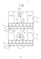
- FIG 3 demonstrates an embodiment of the invention where there are four solar cell layers and three or four photon filters. It should be realised that one of the key inventive concepts of the invention is to get each solar cell layer to work at the band where they have high quantum efficiency (QE), and move not at that band to other solar cell layer that have a better QE at that band. Therefore the QE-wavelength profile of a solar cell layer is of significance to how many solar cell layers are implemented in the design. Typically for semiconductor junctions, the narrower the band is around the optimum energy, the higher the quantum efficiency.
- QE quantum efficiency
- the tandem solar cell comprises several solar cell layers 200, 201, 202, 203, and in between two solar cell layers there is a photon filter, 100, 101, 102.
- the photon filters are tuned so, that they will trap only those photons that are at an energy where the solar cell layer is working at a good quantum efficiency (QE), ideally close to 1.
- QE quantum efficiency
- the rest of the photons are simply passed to the next layer by the photon filter.
- the solar cell layers 200, 201, 202 are preferably very thin, or otherwise designed so that there is minimal interaction between the solar cell and the photon population at energies where the quantum efficiency is NOT that good, i.e. far from unity.
- the last solar cell layer i.e.
- 203 in this case can be thick. It may also have a reflective mirror on the side opposite to the incident side of sunlight, or a photon filter 103 that may be designed to let heat photons out, but trap those photons with photovoltaic band gap absorption potential, i.e. energy enough to be absorbed.
- the first solar cell layer 200 is a GaN layer with a band gap of 3.4 eV (electrovolt).
- the second solar cell layer 201 is a InGaP layer with a band gap of 1.93 eV in some embodiments of the invention.
- the third solar cell layer 202 is a polycrystalline silicon layer, with a band gap at 1.1 eV in some embodiments of the invention.
- the last solar cell layer 203 is a InSb layer with a band gap of 0.17 eV. What could be the cutoff wavelengths ⁇ x s ? In the layer 200 photons with less than 3.4 eV are useless, as they cannot be absorbed into photocurrent.
- the ⁇ x100 should be equivalent to 3.4 eV or similar, i.e. 365 nm, i.e. a UV-mirror that would let photons longer than 365 nm pass through. Consequently, the second InGaP solar cell layer 201 at 1.93eV would require the ⁇ x101 to be equivalent to 1.93 eV or similar, i.e. 643 nm, i.e. a visible light-mirror that would let photons longer than 643 nm pass through.
- the third polymorphic silicon solar cell layer 202 at 1.1 eV would require a 1128 nm for the ⁇ x102 , i.e. a red-IR mirror.
- the photons longer than 1128 nm or similar threshold would be passed to the fourth layer 203 with a InSb band gap of 0.17 eV ⁇ 7301 nm. In some embodiments of the invention this last layer 203 would be made thick, because all the remaining photons should interact in this layer 201.
- embodiment 30 can be freely combined and permuted with embodiments 10, 20, 40 and 50 earlier and later in the text in accordance with the invention.
- Figure 4 displays an exemplary embodiment of the invention in energy space -i.e. spectral space.
- the incident solar spectrum 300 runs from 200 nm in the UV to roughly 2400 nm, the spectrum 300 is a AM 1.5G 1000 W/m 2 solar spectrum typically encountered on Earth.
- the first solar cell layer 200 has a solar cell response that is slightly lower in energy than the GaN and slightly higher in energy than the InGaP. It has a reasonably high QE in between 365-645 nm, i.e. blue light, as shown in the QE plot that is superposed underneath the spectrum 300.
- the photocurrent power spectrum that shows spectral distribution of collected photocurrent power spectrum 400 and therefore energy and power generated by the first solar cell layer 200 is quite similar in shape to the response of the first solar cell layer.
- the photon spectrum 401 will be quite modified when it reaches the first photon filter 100.
- the photon filter 100 will spatiospectrally modulate the photon spectrum 401 in some embodiments of the invention.
- the photon filter 100 will preferably reflect the ⁇ 2 photons with higher energies and shorter wavelengths, i.e. the photons with a shorter wavelength of ⁇ x100 that should be equal to the band gap of the solar cell layer 200 in accordance with the invention.
- the ⁇ 1 photons will be passed to the second solar cell layer 201 by the focusing means or other spatial modulation means, resulting into the spatial component of the modulation, and this layer will again have a different cutoff frequency ⁇ x101 in accordance with the invention in some embodiments.
- the solar cell response 201 converts the photocurrent from this photon population.
- the photon filter 101 will reflect ⁇ 4 photons back to the solar cell layer 201, and the reflector that does this resides on the side facing in the same direction as the sunlight incident side.
- the photon filter 100 will have a reflector 150 around the small apertures 140 that released the ⁇ 1 photons into the second layer 201. This reflector will reflect ⁇ 5 photons back again from the side opposite to the sunlight incident side of photon filter 100, resulting in photon entrapment between photon filters 100, 101, for photons that can interact with the band gap of the second solar cell layer.
- the remaining low energy photons ⁇ 3 are passed onto a third solar cell layer 202 in accordance with the invention in some embodiments, or they are simply released out of the tandem solar cell or left in the lattice in some embodiments of the invention.
- embodiment 40 can be freely combined and permuted with embodiments 10, 20, 30 and/or 50 earlier and later in the text in accordance with the invention.
- Figure 5 shows an embodiment of the operation of the inventive method and device as a flow diagram 50.
- the photons have entered the first solar cell layer 200.
- the photon population traverses through it, with some photons getting absorbed and exciting photocurrent in this solar cell layer.
- the photons After the photons have traversed through the first solar cell layer 200 that is preferably quite thin, they reach the photon filter 100 in phase 600 where the photons with wavelength shorter than ⁇ X100 are reflected back to the first solar cell layer 200.
- the incident and the reflected photons produce the photopower of solar cell 200.
- the photons with wavelength longer than ⁇ X100 are focused by the at least one lens 120.
- the lenses can be of any shape and any material in accordance with the invention, but they can also be replaced by any other focusing means, or in fact by any means capable of splitting the photon populations in the desired way, for example by a unidirectional filter.
- the whole point about focusing the photons passed through is to perform the spatial aspect of the modulation in order to achieve enough reflective surface to the other wall of the photon filter 100 facing the second solar cell layer 201. It is in accordance with the invention to deploy other equivalent means to focusing and spatial modulation in some embodiments.
- phase 620 photons with wavelength longer than ⁇ X100 enter the solar cell 201 through at least one aperture 140, which are typically very small in order to maximise the reflective area 150 of the other wall of the photon filter 100 facing the second solar cell layer 201. Some of these incident photons now generate photopower from second solar cell layer 201.
- phase 630 the photons with wavelength shorter than ⁇ X101 are reflected by the photon filter 101. These photons are thus simply reflected back to the second solar cell layer 201. Some of these reflected photons are absorbed and produce photopower of solar cell 201.
- the reflector 150 of photon filter 100 is designed to simply reflect back all the photons or as many photons as possible on as wide a band as possible in accordance with the invention.
- phase 630 there will now be a photon population bouncing back and forth between the photon filters 100, 101 in accordance with the invention. This photon entrapment gives several opportunities for the photons to get absorbed into the second solar cell layer 201.
- phase 640 the photons that no longer have a chance of being converted to photocurrent, are focused by the lens 121 or other focusing means. It makes sense to adjust the cut off ⁇ X101 so that it reflects back all those photons that do have a chance of getting absorbed in the second solar cell layer 201, but naturally ⁇ X101 can be selected otherwise in accordance with the invention, based on other design criteria for example.
- phase 650 the photons with wavelength longer than ⁇ X101 enter the solar cell 202 preferably from small apertures 141 in the wall of the photon filter 101 facing the third solar cell layer 202.
- the process repeats in the third solar cell layer 202 with the same aforementioned principle albeit at longer wavelengths to generate the photopower of the solar cell 202.
- the embodiment 50 can be freely combined and permuted with embodiments 10, 20, 30 and 40 earlier in the text in accordance with the invention.
- intra band gap semiconductor junctions such as quantum cascade semiconductor junctions can be used to achieve the desired photoelectric properties for a particular solar cell layer in accordance with the invention.
- the solar cells of the invention need not be necessarily square or flat, indeed they can be realised in any shape, for example spherical shape in some embodiments, as described in FI20070743 Thermodynamically shielded solar cell & counterparts or otherwise.
- the solar cell or tandem solar cell systems of the invention can be realised in any size, from nanometer scale structures to large structures.
- the invention has been described here so that the highest band gap solar cell and the highest band pass filter is the first incident to the sunlight. It should be noted that the invention can also be implemented in the reverse order, i.e. having the smaller energy solar cell layers and filters first in some embodiments. Indeed the band gaps of the solar cell layers may be in any order in some embodiments of the invention, the main point is that these solar cell layers work with photons that are at an energy at which the solar cell layer has a good QE, and DO NOT work with photons that are at an energy where the QE is poor.
- the highest band gap material first and the conduction of the filtering and band gaps in an order of high-to-low when moving from the incident sunlight side to the back of the tandem solar cell is preferable in some embodiments of the invention, because this produces the smallest number of photoelectric absorptions per the first photoelectric unit of energy generated.
- the use of the bias voltage as described in FI20070264 is preferable in especially the lower solar cell layers in some embodiments of the invention to achieve photoelectric conversion at very low band gaps.
- the optical concentration and convective, conductive and/or radiative shielding solutions of FI20070743 can be implemented in a very useful way to ensure high photon fluxes in accordance with the invention in some embodiments.
- the software design method of FI20070801 can be used to design some of the tandem cells in accordance with the invention.
- Some of the cost reducing embodiments of EP 09154530.1 can be combined with the embodiments of the present invention. Many useful embodiments can thus be derived from combining the embodiments of these five patent applications from the same inventor that are all directed to the same theme: providing a photoelectric solution to the global energy problem.
- the invention has been explained above with reference to the aforementioned embodiments and several commercial and industrial advantages have been demonstrated.
- the methods and arrangements of the invention allow the construction of a solar cell where a huge number of very thin solar cell layers each work at nearly 100% quantum efficiency, because the inventive photon filters restrict the photon population to the most efficient bands of the solar cell layers, and therefore a practically ideal solar cell delivering power close to the solar constant 1.37 kW / m 2 in space and roughly 1 kW / m 2 on Earth is made possible by the invention.
Landscapes
- Photovoltaic Devices (AREA)
Applications Claiming Priority (1)
| Application Number | Priority Date | Filing Date | Title |
|---|---|---|---|
| EP09162378A EP2261996B8 (fr) | 2009-06-10 | 2009-06-10 | Cellule solaire haute puissance |
Related Parent Applications (1)
| Application Number | Title | Priority Date | Filing Date |
|---|---|---|---|
| EP09162378.5 Division | 2009-06-10 |
Publications (1)
| Publication Number | Publication Date |
|---|---|
| EP2360742A2 true EP2360742A2 (fr) | 2011-08-24 |
Family
ID=41503742
Family Applications (3)
| Application Number | Title | Priority Date | Filing Date |
|---|---|---|---|
| EP11165416A Withdrawn EP2360742A2 (fr) | 2009-06-10 | 2009-06-10 | Procédé et supports pour cellule solaire haute puissance |
| EP09162378A Active EP2261996B8 (fr) | 2009-06-10 | 2009-06-10 | Cellule solaire haute puissance |
| EP10726456A Withdrawn EP2441092A2 (fr) | 2009-06-10 | 2010-06-07 | Procédé et supports pour cellule solaire haute puissance |
Family Applications After (2)
| Application Number | Title | Priority Date | Filing Date |
|---|---|---|---|
| EP09162378A Active EP2261996B8 (fr) | 2009-06-10 | 2009-06-10 | Cellule solaire haute puissance |
| EP10726456A Withdrawn EP2441092A2 (fr) | 2009-06-10 | 2010-06-07 | Procédé et supports pour cellule solaire haute puissance |
Country Status (11)
| Country | Link |
|---|---|
| US (4) | US8198530B2 (fr) |
| EP (3) | EP2360742A2 (fr) |
| JP (1) | JP2012529760A (fr) |
| KR (1) | KR20120087874A (fr) |
| CN (1) | CN102428575A (fr) |
| AT (1) | ATE509375T1 (fr) |
| AU (1) | AU2010257562A1 (fr) |
| CA (1) | CA2766686A1 (fr) |
| DK (1) | DK2261996T3 (fr) |
| ES (1) | ES2363580T3 (fr) |
| WO (1) | WO2010142626A2 (fr) |
Families Citing this family (18)
| Publication number | Priority date | Publication date | Assignee | Title |
|---|---|---|---|---|
| EP2302688A1 (fr) * | 2009-09-23 | 2011-03-30 | Robert Bosch GmbH | Procédé de fabrication d'un substrat doté d'une couche de filtre d'interférence colorée, ce substrat comprenant une couche de filtre d'interférence colorée, l'utilisation de ce substrat comme cellule solaire colorée ou comme module solaire coloré ou comme composant de celui-ci et un faisceau comprenant au moins deux de ces substrats |
| US8217258B2 (en) | 2010-07-09 | 2012-07-10 | Ostendo Technologies, Inc. | Alternating bias hot carrier solar cells |
| EP2523369A1 (fr) | 2011-05-12 | 2012-11-14 | Mikko Väänänen | Station de base comprenant des moyens pour communication optique en espace libre |
| JP2013179297A (ja) * | 2012-02-10 | 2013-09-09 | Tokyo Institute Of Technology | 光学制御層を有する太陽電池セル |
| WO2013132297A1 (fr) * | 2012-03-08 | 2013-09-12 | Siu Chung Tam | Dispositif photovoltaïque |
| JP2014060382A (ja) * | 2012-08-20 | 2014-04-03 | Toshiba Corp | 光電変換素子、光電変換システムおよび光電変換素子の製造方法 |
| US9812867B2 (en) | 2015-06-12 | 2017-11-07 | Black Night Enterprises, Inc. | Capacitor enhanced multi-element photovoltaic cell |
| US9899550B2 (en) | 2015-08-12 | 2018-02-20 | Toyota Motor Engineering & Manufacturing North America, Inc. | Electric power transfer system using optical power transfer |
| EP3358637A4 (fr) | 2015-09-30 | 2019-06-19 | Kaneka Corporation | Dispositif de conversion photoélectrique multi-jonction et module de conversion photoélectrique |
| CN108613412A (zh) * | 2017-02-05 | 2018-10-02 | 鞍钢股份有限公司 | 一种太阳能诱发激光装置及方法 |
| CN107800030A (zh) * | 2017-10-20 | 2018-03-13 | 鞍钢未来钢铁研究院有限公司 | 一种太阳能诱发激光装置及方法 |
| US20210367091A1 (en) * | 2017-11-21 | 2021-11-25 | Technion Research & Development Foundation Limited | Harvesting of energy from diverse wavelengths |
| ES2718705B2 (es) * | 2018-01-03 | 2020-10-02 | Blue Solar Filters Sl | Metodo de configuracion de un filtro multicapa de separacion espectral para aplicaciones solares fotovoltaicas y termicas, filtro y central de generacion asociados a dicho metodo |
| US11709383B2 (en) * | 2018-06-12 | 2023-07-25 | Raymond Hoheisel | Optical communication and power generation device and method |
| EP3977513A4 (fr) * | 2019-05-29 | 2023-06-28 | North Carolina State University | Cellules solaires organiques en tandem transparentes et thermo-isolantes |
| WO2022103509A2 (fr) * | 2020-09-30 | 2022-05-19 | Howe Industries Llc | Système de propulsion thermique solaire thermasat |
| TWI799118B (zh) * | 2022-01-28 | 2023-04-11 | 勝慧科技有限公司 | 雙能區光電效應電極耦合的雙異質接面太陽能電池及其製造方法 |
| US12501740B2 (en) | 2023-10-30 | 2025-12-16 | The Adt Security Corporation | Photodiodes and light emitting diodes |
Citations (5)
| Publication number | Priority date | Publication date | Assignee | Title |
|---|---|---|---|---|
| US6320117B1 (en) | 1999-06-29 | 2001-11-20 | Xoptix, Inc. | Transparent solar cell and method of fabrication |
| US6689949B2 (en) | 2002-05-17 | 2004-02-10 | United Innovations, Inc. | Concentrating photovoltaic cavity converters for extreme solar-to-electric conversion efficiencies |
| EP1724841A1 (fr) | 2004-03-12 | 2006-11-22 | Kyosemi Corporation | Cellule solaire multicouche |
| FI20070264L (fi) | 2007-04-04 | 2008-10-05 | Suinno Oy | Aktiivinen aurinkokenno ja valmistusmenetelmä |
| US20080251112A1 (en) | 2007-04-10 | 2008-10-16 | Raytheon Company | Concentrating photovoltaic kaleidoscope and method |
Family Cites Families (32)
| Publication number | Priority date | Publication date | Assignee | Title |
|---|---|---|---|---|
| JPS5284435A (en) * | 1976-08-03 | 1977-07-14 | Suwa Seikosha Kk | Battery wrist watch |
| US4188238A (en) * | 1978-07-03 | 1980-02-12 | Owens-Illinois, Inc. | Generation of electrical energy from sunlight, and apparatus |
| JPS58188169A (ja) * | 1982-04-27 | 1983-11-02 | Matsushita Electric Ind Co Ltd | 太陽電池 |
| DE3407980A1 (de) * | 1983-04-20 | 1984-10-25 | Tadashi Tokio/Tokyo Sawafuji | Kristallschallerzeuger |
| JPS60111478A (ja) * | 1983-11-22 | 1985-06-17 | Toshiba Corp | 光起電力装置 |
| JP2717583B2 (ja) * | 1988-11-04 | 1998-02-18 | キヤノン株式会社 | 積層型光起電力素子 |
| JP2738557B2 (ja) * | 1989-03-10 | 1998-04-08 | 三菱電機株式会社 | 多層構造太陽電池 |
| JPH03224898A (ja) * | 1990-01-30 | 1991-10-03 | Mitsubishi Electric Corp | 人工衛星 |
| CN2100660U (zh) * | 1991-08-31 | 1992-04-01 | 马希光 | 可充电太阳能计算机 |
| US5220462A (en) * | 1991-11-15 | 1993-06-15 | Feldman Jr Karl T | Diode glazing with radiant energy trapping |
| JPH09162435A (ja) * | 1995-12-07 | 1997-06-20 | Toppan Printing Co Ltd | 太陽電池用フィルター |
| WO1999049522A1 (fr) * | 1998-03-25 | 1999-09-30 | Tdk Corporation | Module solaire |
| JP2003101059A (ja) * | 2001-09-27 | 2003-04-04 | Sharp Corp | 薄膜太陽電池 |
| US7095050B2 (en) * | 2002-02-28 | 2006-08-22 | Midwest Research Institute | Voltage-matched, monolithic, multi-band-gap devices |
| US7217882B2 (en) * | 2002-05-24 | 2007-05-15 | Cornell Research Foundation, Inc. | Broad spectrum solar cell |
| US7126052B2 (en) * | 2002-10-02 | 2006-10-24 | The Boeing Company | Isoelectronic surfactant induced sublattice disordering in optoelectronic devices |
| WO2004090487A1 (fr) * | 2003-03-26 | 2004-10-21 | Semiconductor Energy Laboratory Co., Ltd. | Capteur optique destine a detecter des faisceaux lumineux provenant de plusieurs directions, dispositif de communication mobile et procede d'affichage |
| WO2005011001A1 (fr) * | 2003-07-24 | 2005-02-03 | Kaneka Corporation | Convertisseur photoelectrique a empilement |
| US20050199280A1 (en) * | 2004-03-12 | 2005-09-15 | Royer George R. | Solar battery |
| DE102005000767A1 (de) * | 2005-01-04 | 2006-07-20 | Rwe Space Solar Power Gmbh | Monolithische Mehrfach-Solarzelle |
| KR101381508B1 (ko) * | 2005-07-15 | 2014-04-04 | 메르크 파텐트 게엠베하 | 회절 호일 |
| US7459880B1 (en) * | 2006-07-24 | 2008-12-02 | George Michel Rosen | Solar generator panel for an electric or hybrid vehicle |
| US7708123B2 (en) * | 2006-08-09 | 2010-05-04 | Tai-Her Yang | Spring device with capability of intermittent random energy accumulator and kinetics release trigger |
| CN101286531A (zh) * | 2007-04-09 | 2008-10-15 | 台达电子工业股份有限公司 | 太阳能电池 |
| ATE504086T1 (de) * | 2007-05-28 | 2011-04-15 | Consiglio Nazionale Ricerche | Fotovoltaikvorrichtung mit verbesserter lichtsammlung |
| US20090078311A1 (en) * | 2007-09-24 | 2009-03-26 | Emcore Corporation | Surfactant Assisted Growth in Barrier Layers In Inverted Metamorphic Multijunction Solar Cells |
| EP2195856A2 (fr) * | 2007-10-01 | 2010-06-16 | Suinno Oy | Pile solaire blindée thermodynamiquement |
| US20090091479A1 (en) * | 2007-10-04 | 2009-04-09 | Motorola, Inc. | Keypad haptic communication |
| KR20100090257A (ko) * | 2007-10-19 | 2010-08-13 | 퀄컴 엠이엠스 테크놀로지스, 인크. | 광기전력 소자가 통합된 디스플레이 |
| BRPI0821371A2 (pt) * | 2007-12-21 | 2015-06-16 | Qualcomm Mems Technologies Inc | Dispositivos fotovoltaicos e respectivo método de fabrico |
| JP2010016936A (ja) * | 2008-07-02 | 2010-01-21 | Casio Comput Co Ltd | 発電装置 |
| EP2226852B8 (fr) | 2009-03-06 | 2011-10-05 | Suinno Solar Oy | Cellule solaire à faible coût |
-
2009
- 2009-06-10 ES ES09162378T patent/ES2363580T3/es active Active
- 2009-06-10 EP EP11165416A patent/EP2360742A2/fr not_active Withdrawn
- 2009-06-10 AT AT09162378T patent/ATE509375T1/de not_active IP Right Cessation
- 2009-06-10 DK DK09162378.5T patent/DK2261996T3/da active
- 2009-06-10 EP EP09162378A patent/EP2261996B8/fr active Active
-
2010
- 2010-06-01 US US12/791,188 patent/US8198530B2/en not_active Expired - Fee Related
- 2010-06-07 AU AU2010257562A patent/AU2010257562A1/en not_active Abandoned
- 2010-06-07 CN CN201080021674XA patent/CN102428575A/zh active Pending
- 2010-06-07 JP JP2012514434A patent/JP2012529760A/ja active Pending
- 2010-06-07 WO PCT/EP2010/057888 patent/WO2010142626A2/fr not_active Ceased
- 2010-06-07 KR KR1020127000677A patent/KR20120087874A/ko not_active Withdrawn
- 2010-06-07 EP EP10726456A patent/EP2441092A2/fr not_active Withdrawn
- 2010-06-07 CA CA2766686A patent/CA2766686A1/fr not_active Abandoned
-
2011
- 2011-03-18 US US13/051,097 patent/US20110168244A1/en not_active Abandoned
-
2021
- 2021-01-04 US US17/140,158 patent/US20210151620A1/en not_active Abandoned
- 2021-02-07 US US17/169,482 patent/US20210343890A1/en not_active Abandoned
Patent Citations (5)
| Publication number | Priority date | Publication date | Assignee | Title |
|---|---|---|---|---|
| US6320117B1 (en) | 1999-06-29 | 2001-11-20 | Xoptix, Inc. | Transparent solar cell and method of fabrication |
| US6689949B2 (en) | 2002-05-17 | 2004-02-10 | United Innovations, Inc. | Concentrating photovoltaic cavity converters for extreme solar-to-electric conversion efficiencies |
| EP1724841A1 (fr) | 2004-03-12 | 2006-11-22 | Kyosemi Corporation | Cellule solaire multicouche |
| FI20070264L (fi) | 2007-04-04 | 2008-10-05 | Suinno Oy | Aktiivinen aurinkokenno ja valmistusmenetelmä |
| US20080251112A1 (en) | 2007-04-10 | 2008-10-16 | Raytheon Company | Concentrating photovoltaic kaleidoscope and method |
Non-Patent Citations (3)
| Title |
|---|
| JAMES P. CAMPBELL ET AL.: "Solar Electricity", THOMAS MARKVART, article "Transparent solar cell and method of fabrication" |
| JAMES P. CAMPBELL ET AL.: "Solar Electricity, Thomas Markvart", article "Transparent solar cell and method of fabrication" |
| PAUL PREUSS: "Research News", LAWRENCE BERKELEY NATIONAL LABORATORY, article "An unexpected discovery could yield a full spectrum solar cell" |
Also Published As
| Publication number | Publication date |
|---|---|
| ES2363580T3 (es) | 2011-08-09 |
| US20210343890A1 (en) | 2021-11-04 |
| EP2261996A1 (fr) | 2010-12-15 |
| US20110168244A1 (en) | 2011-07-14 |
| US8198530B2 (en) | 2012-06-12 |
| CA2766686A1 (fr) | 2010-12-16 |
| DK2261996T3 (da) | 2011-08-29 |
| JP2012529760A (ja) | 2012-11-22 |
| EP2261996B1 (fr) | 2011-05-11 |
| US20210151620A1 (en) | 2021-05-20 |
| US20100313934A1 (en) | 2010-12-16 |
| KR20120087874A (ko) | 2012-08-07 |
| HK1148865A1 (en) | 2011-09-16 |
| EP2261996B8 (fr) | 2011-10-19 |
| WO2010142626A3 (fr) | 2011-08-11 |
| ATE509375T1 (de) | 2011-05-15 |
| CN102428575A (zh) | 2012-04-25 |
| WO2010142626A2 (fr) | 2010-12-16 |
| AU2010257562A1 (en) | 2012-02-02 |
| EP2441092A2 (fr) | 2012-04-18 |
Similar Documents
| Publication | Publication Date | Title |
|---|---|---|
| EP2261996B1 (fr) | Cellule solaire haute puissance | |
| US8153888B2 (en) | Lateral ultra-high efficiency solar cell | |
| US7081584B2 (en) | Solar based electrical energy generation with spectral cooling | |
| US20110048520A1 (en) | High efficiency solar cell with a silicon scavenger cell | |
| JP5626796B2 (ja) | 直列接続型ソーラーセル及びソーラーセルシステム | |
| US20100170557A1 (en) | High Efficiency Solar Cell With Surrounding Silicon Scavenger Cells | |
| US20130037108A1 (en) | Thermodynamically shielded solar cell | |
| US7994417B1 (en) | Optimal cell selection for series connection in Cassegrain PV module | |
| HK1159849A (en) | Method and means for a high power solar cell | |
| HK1148865B (en) | High power solar cell | |
| WO2024157371A1 (fr) | Module de batterie solaire et dispositif de conversion |
Legal Events
| Date | Code | Title | Description |
|---|---|---|---|
| PUAI | Public reference made under article 153(3) epc to a published international application that has entered the european phase |
Free format text: ORIGINAL CODE: 0009012 |
|
| AC | Divisional application: reference to earlier application |
Ref document number: 2261996 Country of ref document: EP Kind code of ref document: P |
|
| AK | Designated contracting states |
Kind code of ref document: A2 Designated state(s): AT BE BG CH CY CZ DE DK EE ES FI FR GB GR HR HU IE IS IT LI LT LU LV MC MK MT NL NO PL PT RO SE SI SK TR |
|
| REG | Reference to a national code |
Ref country code: HK Ref legal event code: DE Ref document number: 1159849 Country of ref document: HK |
|
| STAA | Information on the status of an ep patent application or granted ep patent |
Free format text: STATUS: THE APPLICATION IS DEEMED TO BE WITHDRAWN |
|
| 18D | Application deemed to be withdrawn |
Effective date: 20150106 |
|
| REG | Reference to a national code |
Ref country code: HK Ref legal event code: WD Ref document number: 1159849 Country of ref document: HK |