EP2363511A2 - Gasabgrenzungsfilm, Filmablagerungsverfahren und Filmablagerungsvorrichtung - Google Patents
Gasabgrenzungsfilm, Filmablagerungsverfahren und Filmablagerungsvorrichtung Download PDFInfo
- Publication number
- EP2363511A2 EP2363511A2 EP11154967A EP11154967A EP2363511A2 EP 2363511 A2 EP2363511 A2 EP 2363511A2 EP 11154967 A EP11154967 A EP 11154967A EP 11154967 A EP11154967 A EP 11154967A EP 2363511 A2 EP2363511 A2 EP 2363511A2
- Authority
- EP
- European Patent Office
- Prior art keywords
- base film
- film
- film deposition
- silicon nitride
- gas
- Prior art date
- Legal status (The legal status is an assumption and is not a legal conclusion. Google has not performed a legal analysis and makes no representation as to the accuracy of the status listed.)
- Granted
Links
- 230000004888 barrier function Effects 0.000 title claims abstract description 82
- 238000000151 deposition Methods 0.000 title claims description 160
- 230000008021 deposition Effects 0.000 title claims description 131
- 229910052581 Si3N4 Inorganic materials 0.000 claims abstract description 87
- HQVNEWCFYHHQES-UHFFFAOYSA-N silicon nitride Chemical compound N12[Si]34N5[Si]62N3[Si]51N64 HQVNEWCFYHHQES-UHFFFAOYSA-N 0.000 claims abstract description 87
- 239000000463 material Substances 0.000 claims description 90
- 229910000077 silane Inorganic materials 0.000 claims description 25
- 238000011144 upstream manufacturing Methods 0.000 claims description 20
- 238000000623 plasma-assisted chemical vapour deposition Methods 0.000 claims description 14
- 230000000903 blocking effect Effects 0.000 claims description 7
- 230000002093 peripheral effect Effects 0.000 claims description 4
- 238000007599 discharging Methods 0.000 claims description 3
- 239000004460 silage Substances 0.000 claims 1
- 239000010408 film Substances 0.000 description 310
- 239000007789 gas Substances 0.000 description 188
- 239000010410 layer Substances 0.000 description 112
- -1 silane radicals Chemical class 0.000 description 50
- 229910003828 SiH3 Inorganic materials 0.000 description 22
- BLRPTPMANUNPDV-UHFFFAOYSA-N Silane Chemical compound [SiH4] BLRPTPMANUNPDV-UHFFFAOYSA-N 0.000 description 13
- 230000005284 excitation Effects 0.000 description 12
- 238000004519 manufacturing process Methods 0.000 description 12
- 238000000034 method Methods 0.000 description 12
- 230000003647 oxidation Effects 0.000 description 12
- 238000007254 oxidation reaction Methods 0.000 description 12
- OLRJXMHANKMLTD-UHFFFAOYSA-N silyl Chemical compound [SiH3] OLRJXMHANKMLTD-UHFFFAOYSA-N 0.000 description 8
- QGZKDVFQNNGYKY-UHFFFAOYSA-N Ammonia Chemical compound N QGZKDVFQNNGYKY-UHFFFAOYSA-N 0.000 description 7
- XMIJDTGORVPYLW-UHFFFAOYSA-N [SiH2] Chemical compound [SiH2] XMIJDTGORVPYLW-UHFFFAOYSA-N 0.000 description 6
- 230000007423 decrease Effects 0.000 description 6
- 238000003860 storage Methods 0.000 description 6
- IJGRMHOSHXDMSA-UHFFFAOYSA-N Atomic nitrogen Chemical compound N#N IJGRMHOSHXDMSA-UHFFFAOYSA-N 0.000 description 5
- UFHFLCQGNIYNRP-UHFFFAOYSA-N Hydrogen Chemical compound [H][H] UFHFLCQGNIYNRP-UHFFFAOYSA-N 0.000 description 5
- 238000005192 partition Methods 0.000 description 5
- 238000005268 plasma chemical vapour deposition Methods 0.000 description 5
- 238000004833 X-ray photoelectron spectroscopy Methods 0.000 description 4
- IJOOHPMOJXWVHK-UHFFFAOYSA-N chlorotrimethylsilane Chemical compound C[Si](C)(C)Cl IJOOHPMOJXWVHK-UHFFFAOYSA-N 0.000 description 4
- 230000000052 comparative effect Effects 0.000 description 4
- 150000003254 radicals Chemical class 0.000 description 4
- 125000000954 2-hydroxyethyl group Chemical group [H]C([*])([H])C([H])([H])O[H] 0.000 description 3
- BOTDANWDWHJENH-UHFFFAOYSA-N Tetraethyl orthosilicate Chemical compound CCO[Si](OCC)(OCC)OCC BOTDANWDWHJENH-UHFFFAOYSA-N 0.000 description 3
- 230000005540 biological transmission Effects 0.000 description 3
- 229910001873 dinitrogen Inorganic materials 0.000 description 3
- 238000009826 distribution Methods 0.000 description 3
- GRVDJDISBSALJP-UHFFFAOYSA-N methyloxidanyl Chemical compound [O]C GRVDJDISBSALJP-UHFFFAOYSA-N 0.000 description 3
- 229920005989 resin Polymers 0.000 description 3
- 239000011347 resin Substances 0.000 description 3
- CZDYPVPMEAXLPK-UHFFFAOYSA-N tetramethylsilane Chemical compound C[Si](C)(C)C CZDYPVPMEAXLPK-UHFFFAOYSA-N 0.000 description 3
- AQRLNPVMDITEJU-UHFFFAOYSA-N triethylsilane Chemical compound CC[SiH](CC)CC AQRLNPVMDITEJU-UHFFFAOYSA-N 0.000 description 3
- 238000001771 vacuum deposition Methods 0.000 description 3
- XKRFYHLGVUSROY-UHFFFAOYSA-N Argon Chemical compound [Ar] XKRFYHLGVUSROY-UHFFFAOYSA-N 0.000 description 2
- VYPSYNLAJGMNEJ-UHFFFAOYSA-N Silicium dioxide Chemical compound O=[Si]=O VYPSYNLAJGMNEJ-UHFFFAOYSA-N 0.000 description 2
- 230000002411 adverse Effects 0.000 description 2
- 230000008859 change Effects 0.000 description 2
- 238000001816 cooling Methods 0.000 description 2
- 238000005137 deposition process Methods 0.000 description 2
- LIKFHECYJZWXFJ-UHFFFAOYSA-N dimethyldichlorosilane Chemical compound C[Si](C)(Cl)Cl LIKFHECYJZWXFJ-UHFFFAOYSA-N 0.000 description 2
- 238000001678 elastic recoil detection analysis Methods 0.000 description 2
- 238000010438 heat treatment Methods 0.000 description 2
- 230000006872 improvement Effects 0.000 description 2
- 238000009616 inductively coupled plasma Methods 0.000 description 2
- 239000004973 liquid crystal related substance Substances 0.000 description 2
- UIUXUFNYAYAMOE-UHFFFAOYSA-N methylsilane Chemical compound [SiH3]C UIUXUFNYAYAMOE-UHFFFAOYSA-N 0.000 description 2
- JLUFWMXJHAVVNN-UHFFFAOYSA-N methyltrichlorosilane Chemical compound C[Si](Cl)(Cl)Cl JLUFWMXJHAVVNN-UHFFFAOYSA-N 0.000 description 2
- 239000002985 plastic film Substances 0.000 description 2
- 229920006255 plastic film Polymers 0.000 description 2
- 239000011112 polyethylene naphthalate Substances 0.000 description 2
- 230000008569 process Effects 0.000 description 2
- 230000009467 reduction Effects 0.000 description 2
- 229910052814 silicon oxide Inorganic materials 0.000 description 2
- PQDJYEQOELDLCP-UHFFFAOYSA-N trimethylsilane Chemical compound C[SiH](C)C PQDJYEQOELDLCP-UHFFFAOYSA-N 0.000 description 2
- REJKHFAZHZLNOP-UHFFFAOYSA-N (tert-butylamino)silicon Chemical compound CC(C)(C)N[Si] REJKHFAZHZLNOP-UHFFFAOYSA-N 0.000 description 1
- CHBOSHOWERDCMH-UHFFFAOYSA-N 1-chloro-2,2-bis(4-chlorophenyl)ethane Chemical compound C=1C=C(Cl)C=CC=1C(CCl)C1=CC=C(Cl)C=C1 CHBOSHOWERDCMH-UHFFFAOYSA-N 0.000 description 1
- OYPRJOBELJOOCE-UHFFFAOYSA-N Calcium Chemical compound [Ca] OYPRJOBELJOOCE-UHFFFAOYSA-N 0.000 description 1
- 239000004952 Polyamide Substances 0.000 description 1
- 239000004698 Polyethylene Substances 0.000 description 1
- 239000004642 Polyimide Substances 0.000 description 1
- 239000004743 Polypropylene Substances 0.000 description 1
- 239000004793 Polystyrene Substances 0.000 description 1
- XUIMIQQOPSSXEZ-UHFFFAOYSA-N Silicon Chemical compound [Si] XUIMIQQOPSSXEZ-UHFFFAOYSA-N 0.000 description 1
- 239000012790 adhesive layer Substances 0.000 description 1
- 238000004458 analytical method Methods 0.000 description 1
- 229910052786 argon Inorganic materials 0.000 description 1
- QVGXLLKOCUKJST-UHFFFAOYSA-N atomic oxygen Chemical compound [O] QVGXLLKOCUKJST-UHFFFAOYSA-N 0.000 description 1
- 230000009286 beneficial effect Effects 0.000 description 1
- 230000015572 biosynthetic process Effects 0.000 description 1
- 229910052791 calcium Inorganic materials 0.000 description 1
- 239000011575 calcium Substances 0.000 description 1
- 238000006243 chemical reaction Methods 0.000 description 1
- 239000003795 chemical substances by application Substances 0.000 description 1
- 239000011248 coating agent Substances 0.000 description 1
- 238000000576 coating method Methods 0.000 description 1
- 238000007796 conventional method Methods 0.000 description 1
- 230000007797 corrosion Effects 0.000 description 1
- 238000005260 corrosion Methods 0.000 description 1
- 230000003247 decreasing effect Effects 0.000 description 1
- 230000006866 deterioration Effects 0.000 description 1
- PFMKUUJQLUQKHT-UHFFFAOYSA-N dichloro(ethyl)silicon Chemical compound CC[Si](Cl)Cl PFMKUUJQLUQKHT-UHFFFAOYSA-N 0.000 description 1
- KTQYJQFGNYHXMB-UHFFFAOYSA-N dichloro(methyl)silicon Chemical compound C[Si](Cl)Cl KTQYJQFGNYHXMB-UHFFFAOYSA-N 0.000 description 1
- NBBQQQJUOYRZCA-UHFFFAOYSA-N diethoxymethylsilane Chemical compound CCOC([SiH3])OCC NBBQQQJUOYRZCA-UHFFFAOYSA-N 0.000 description 1
- UCXUKTLCVSGCNR-UHFFFAOYSA-N diethylsilane Chemical compound CC[SiH2]CC UCXUKTLCVSGCNR-UHFFFAOYSA-N 0.000 description 1
- 239000003085 diluting agent Substances 0.000 description 1
- JJQZDUKDJDQPMQ-UHFFFAOYSA-N dimethoxy(dimethyl)silane Chemical compound CO[Si](C)(C)OC JJQZDUKDJDQPMQ-UHFFFAOYSA-N 0.000 description 1
- YYLGKUPAFFKGRQ-UHFFFAOYSA-N dimethyldiethoxysilane Chemical compound CCO[Si](C)(C)OCC YYLGKUPAFFKGRQ-UHFFFAOYSA-N 0.000 description 1
- UBHZUDXTHNMNLD-UHFFFAOYSA-N dimethylsilane Chemical compound C[SiH2]C UBHZUDXTHNMNLD-UHFFFAOYSA-N 0.000 description 1
- JZZIHCLFHIXETF-UHFFFAOYSA-N dimethylsilicon Chemical compound C[Si]C JZZIHCLFHIXETF-UHFFFAOYSA-N 0.000 description 1
- 230000000694 effects Effects 0.000 description 1
- 230000005611 electricity Effects 0.000 description 1
- 238000001704 evaporation Methods 0.000 description 1
- 230000008020 evaporation Effects 0.000 description 1
- 238000002474 experimental method Methods 0.000 description 1
- 239000007888 film coating Substances 0.000 description 1
- 238000009501 film coating Methods 0.000 description 1
- 239000001307 helium Substances 0.000 description 1
- 229910052734 helium Inorganic materials 0.000 description 1
- SWQJXJOGLNCZEY-UHFFFAOYSA-N helium atom Chemical compound [He] SWQJXJOGLNCZEY-UHFFFAOYSA-N 0.000 description 1
- UQEAIHBTYFGYIE-UHFFFAOYSA-N hexamethyldisiloxane Chemical compound C[Si](C)(C)O[Si](C)(C)C UQEAIHBTYFGYIE-UHFFFAOYSA-N 0.000 description 1
- 239000001257 hydrogen Substances 0.000 description 1
- 229910052739 hydrogen Inorganic materials 0.000 description 1
- 238000009413 insulation Methods 0.000 description 1
- 238000005259 measurement Methods 0.000 description 1
- 239000005055 methyl trichlorosilane Substances 0.000 description 1
- 239000005048 methyldichlorosilane Substances 0.000 description 1
- BFXIKLCIZHOAAZ-UHFFFAOYSA-N methyltrimethoxysilane Chemical compound CO[Si](C)(OC)OC BFXIKLCIZHOAAZ-UHFFFAOYSA-N 0.000 description 1
- 238000012986 modification Methods 0.000 description 1
- 230000004048 modification Effects 0.000 description 1
- 229910052757 nitrogen Inorganic materials 0.000 description 1
- 150000002831 nitrogen free-radicals Chemical class 0.000 description 1
- 229910000069 nitrogen hydride Inorganic materials 0.000 description 1
- 230000003287 optical effect Effects 0.000 description 1
- 239000011368 organic material Substances 0.000 description 1
- TWNQGVIAIRXVLR-UHFFFAOYSA-N oxo(oxoalumanyloxy)alumane Chemical compound O=[Al]O[Al]=O TWNQGVIAIRXVLR-UHFFFAOYSA-N 0.000 description 1
- 239000001301 oxygen Substances 0.000 description 1
- 229910052760 oxygen Inorganic materials 0.000 description 1
- 239000005022 packaging material Substances 0.000 description 1
- 238000009832 plasma treatment Methods 0.000 description 1
- 229920003207 poly(ethylene-2,6-naphthalate) Polymers 0.000 description 1
- 229920000058 polyacrylate Polymers 0.000 description 1
- 229920002239 polyacrylonitrile Polymers 0.000 description 1
- 229920002647 polyamide Polymers 0.000 description 1
- 229920000515 polycarbonate Polymers 0.000 description 1
- 239000004417 polycarbonate Substances 0.000 description 1
- 229920000573 polyethylene Polymers 0.000 description 1
- 229920000139 polyethylene terephthalate Polymers 0.000 description 1
- 239000005020 polyethylene terephthalate Substances 0.000 description 1
- 229920001721 polyimide Polymers 0.000 description 1
- 229920000193 polymethacrylate Polymers 0.000 description 1
- 229920001155 polypropylene Polymers 0.000 description 1
- 229920002223 polystyrene Polymers 0.000 description 1
- 229920000915 polyvinyl chloride Polymers 0.000 description 1
- 239000004800 polyvinyl chloride Substances 0.000 description 1
- 239000011241 protective layer Substances 0.000 description 1
- 239000003507 refrigerant Substances 0.000 description 1
- 230000001105 regulatory effect Effects 0.000 description 1
- 238000005001 rutherford backscattering spectroscopy Methods 0.000 description 1
- 239000004065 semiconductor Substances 0.000 description 1
- 229910052710 silicon Inorganic materials 0.000 description 1
- 239000010703 silicon Substances 0.000 description 1
- 238000004088 simulation Methods 0.000 description 1
- 239000002356 single layer Substances 0.000 description 1
- 238000004544 sputter deposition Methods 0.000 description 1
- 239000000126 substance Substances 0.000 description 1
- 230000003746 surface roughness Effects 0.000 description 1
- 238000004381 surface treatment Methods 0.000 description 1
- 238000012360 testing method Methods 0.000 description 1
- LFQCEHFDDXELDD-UHFFFAOYSA-N tetramethyl orthosilicate Chemical compound CO[Si](OC)(OC)OC LFQCEHFDDXELDD-UHFFFAOYSA-N 0.000 description 1
- 239000010409 thin film Substances 0.000 description 1
- CPUDPFPXCZDNGI-UHFFFAOYSA-N triethoxy(methyl)silane Chemical compound CCO[Si](C)(OCC)OCC CPUDPFPXCZDNGI-UHFFFAOYSA-N 0.000 description 1
- QQQSFSZALRVCSZ-UHFFFAOYSA-N triethoxysilane Chemical compound CCO[SiH](OCC)OCC QQQSFSZALRVCSZ-UHFFFAOYSA-N 0.000 description 1
- PKDCQJMRWCHQOH-UHFFFAOYSA-N triethoxysilicon Chemical compound CCO[Si](OCC)OCC PKDCQJMRWCHQOH-UHFFFAOYSA-N 0.000 description 1
- QXTIBZLKQPJVII-UHFFFAOYSA-N triethylsilicon Chemical compound CC[Si](CC)CC QXTIBZLKQPJVII-UHFFFAOYSA-N 0.000 description 1
- 239000005051 trimethylchlorosilane Substances 0.000 description 1
- 229940094989 trimethylsilane Drugs 0.000 description 1
- 238000007740 vapor deposition Methods 0.000 description 1
- XLYOFNOQVPJJNP-UHFFFAOYSA-N water Chemical compound O XLYOFNOQVPJJNP-UHFFFAOYSA-N 0.000 description 1
- 238000004804 winding Methods 0.000 description 1
Images


Classifications
-
- C—CHEMISTRY; METALLURGY
- C23—COATING METALLIC MATERIAL; COATING MATERIAL WITH METALLIC MATERIAL; CHEMICAL SURFACE TREATMENT; DIFFUSION TREATMENT OF METALLIC MATERIAL; COATING BY VACUUM EVAPORATION, BY SPUTTERING, BY ION IMPLANTATION OR BY CHEMICAL VAPOUR DEPOSITION, IN GENERAL; INHIBITING CORROSION OF METALLIC MATERIAL OR INCRUSTATION IN GENERAL
- C23C—COATING METALLIC MATERIAL; COATING MATERIAL WITH METALLIC MATERIAL; SURFACE TREATMENT OF METALLIC MATERIAL BY DIFFUSION INTO THE SURFACE, BY CHEMICAL CONVERSION OR SUBSTITUTION; COATING BY VACUUM EVAPORATION, BY SPUTTERING, BY ION IMPLANTATION OR BY CHEMICAL VAPOUR DEPOSITION, IN GENERAL
- C23C16/00—Chemical coating by decomposition of gaseous compounds, without leaving reaction products of surface material in the coating, i.e. chemical vapour deposition [CVD] processes
- C23C16/44—Chemical coating by decomposition of gaseous compounds, without leaving reaction products of surface material in the coating, i.e. chemical vapour deposition [CVD] processes characterised by the method of coating
- C23C16/54—Apparatus specially adapted for continuous coating
- C23C16/545—Apparatus specially adapted for continuous coating for coating elongated substrates
-
- C—CHEMISTRY; METALLURGY
- C23—COATING METALLIC MATERIAL; COATING MATERIAL WITH METALLIC MATERIAL; CHEMICAL SURFACE TREATMENT; DIFFUSION TREATMENT OF METALLIC MATERIAL; COATING BY VACUUM EVAPORATION, BY SPUTTERING, BY ION IMPLANTATION OR BY CHEMICAL VAPOUR DEPOSITION, IN GENERAL; INHIBITING CORROSION OF METALLIC MATERIAL OR INCRUSTATION IN GENERAL
- C23C—COATING METALLIC MATERIAL; COATING MATERIAL WITH METALLIC MATERIAL; SURFACE TREATMENT OF METALLIC MATERIAL BY DIFFUSION INTO THE SURFACE, BY CHEMICAL CONVERSION OR SUBSTITUTION; COATING BY VACUUM EVAPORATION, BY SPUTTERING, BY ION IMPLANTATION OR BY CHEMICAL VAPOUR DEPOSITION, IN GENERAL
- C23C16/00—Chemical coating by decomposition of gaseous compounds, without leaving reaction products of surface material in the coating, i.e. chemical vapour deposition [CVD] processes
- C23C16/22—Chemical coating by decomposition of gaseous compounds, without leaving reaction products of surface material in the coating, i.e. chemical vapour deposition [CVD] processes characterised by the deposition of inorganic material, other than metallic material
- C23C16/30—Deposition of compounds, mixtures or solid solutions, e.g. borides, carbides, nitrides
- C23C16/34—Nitrides
- C23C16/345—Silicon nitride
-
- C—CHEMISTRY; METALLURGY
- C23—COATING METALLIC MATERIAL; COATING MATERIAL WITH METALLIC MATERIAL; CHEMICAL SURFACE TREATMENT; DIFFUSION TREATMENT OF METALLIC MATERIAL; COATING BY VACUUM EVAPORATION, BY SPUTTERING, BY ION IMPLANTATION OR BY CHEMICAL VAPOUR DEPOSITION, IN GENERAL; INHIBITING CORROSION OF METALLIC MATERIAL OR INCRUSTATION IN GENERAL
- C23C—COATING METALLIC MATERIAL; COATING MATERIAL WITH METALLIC MATERIAL; SURFACE TREATMENT OF METALLIC MATERIAL BY DIFFUSION INTO THE SURFACE, BY CHEMICAL CONVERSION OR SUBSTITUTION; COATING BY VACUUM EVAPORATION, BY SPUTTERING, BY ION IMPLANTATION OR BY CHEMICAL VAPOUR DEPOSITION, IN GENERAL
- C23C16/00—Chemical coating by decomposition of gaseous compounds, without leaving reaction products of surface material in the coating, i.e. chemical vapour deposition [CVD] processes
- C23C16/44—Chemical coating by decomposition of gaseous compounds, without leaving reaction products of surface material in the coating, i.e. chemical vapour deposition [CVD] processes characterised by the method of coating
- C23C16/455—Chemical coating by decomposition of gaseous compounds, without leaving reaction products of surface material in the coating, i.e. chemical vapour deposition [CVD] processes characterised by the method of coating characterised by the method used for introducing gases into reaction chamber or for modifying gas flows in reaction chamber
-
- C—CHEMISTRY; METALLURGY
- C23—COATING METALLIC MATERIAL; COATING MATERIAL WITH METALLIC MATERIAL; CHEMICAL SURFACE TREATMENT; DIFFUSION TREATMENT OF METALLIC MATERIAL; COATING BY VACUUM EVAPORATION, BY SPUTTERING, BY ION IMPLANTATION OR BY CHEMICAL VAPOUR DEPOSITION, IN GENERAL; INHIBITING CORROSION OF METALLIC MATERIAL OR INCRUSTATION IN GENERAL
- C23C—COATING METALLIC MATERIAL; COATING MATERIAL WITH METALLIC MATERIAL; SURFACE TREATMENT OF METALLIC MATERIAL BY DIFFUSION INTO THE SURFACE, BY CHEMICAL CONVERSION OR SUBSTITUTION; COATING BY VACUUM EVAPORATION, BY SPUTTERING, BY ION IMPLANTATION OR BY CHEMICAL VAPOUR DEPOSITION, IN GENERAL
- C23C16/00—Chemical coating by decomposition of gaseous compounds, without leaving reaction products of surface material in the coating, i.e. chemical vapour deposition [CVD] processes
- C23C16/44—Chemical coating by decomposition of gaseous compounds, without leaving reaction products of surface material in the coating, i.e. chemical vapour deposition [CVD] processes characterised by the method of coating
- C23C16/455—Chemical coating by decomposition of gaseous compounds, without leaving reaction products of surface material in the coating, i.e. chemical vapour deposition [CVD] processes characterised by the method of coating characterised by the method used for introducing gases into reaction chamber or for modifying gas flows in reaction chamber
- C23C16/45563—Gas nozzles
- C23C16/45565—Shower nozzles
-
- C—CHEMISTRY; METALLURGY
- C23—COATING METALLIC MATERIAL; COATING MATERIAL WITH METALLIC MATERIAL; CHEMICAL SURFACE TREATMENT; DIFFUSION TREATMENT OF METALLIC MATERIAL; COATING BY VACUUM EVAPORATION, BY SPUTTERING, BY ION IMPLANTATION OR BY CHEMICAL VAPOUR DEPOSITION, IN GENERAL; INHIBITING CORROSION OF METALLIC MATERIAL OR INCRUSTATION IN GENERAL
- C23C—COATING METALLIC MATERIAL; COATING MATERIAL WITH METALLIC MATERIAL; SURFACE TREATMENT OF METALLIC MATERIAL BY DIFFUSION INTO THE SURFACE, BY CHEMICAL CONVERSION OR SUBSTITUTION; COATING BY VACUUM EVAPORATION, BY SPUTTERING, BY ION IMPLANTATION OR BY CHEMICAL VAPOUR DEPOSITION, IN GENERAL
- C23C16/00—Chemical coating by decomposition of gaseous compounds, without leaving reaction products of surface material in the coating, i.e. chemical vapour deposition [CVD] processes
- C23C16/44—Chemical coating by decomposition of gaseous compounds, without leaving reaction products of surface material in the coating, i.e. chemical vapour deposition [CVD] processes characterised by the method of coating
- C23C16/455—Chemical coating by decomposition of gaseous compounds, without leaving reaction products of surface material in the coating, i.e. chemical vapour deposition [CVD] processes characterised by the method of coating characterised by the method used for introducing gases into reaction chamber or for modifying gas flows in reaction chamber
- C23C16/45587—Mechanical means for changing the gas flow
-
- C—CHEMISTRY; METALLURGY
- C23—COATING METALLIC MATERIAL; COATING MATERIAL WITH METALLIC MATERIAL; CHEMICAL SURFACE TREATMENT; DIFFUSION TREATMENT OF METALLIC MATERIAL; COATING BY VACUUM EVAPORATION, BY SPUTTERING, BY ION IMPLANTATION OR BY CHEMICAL VAPOUR DEPOSITION, IN GENERAL; INHIBITING CORROSION OF METALLIC MATERIAL OR INCRUSTATION IN GENERAL
- C23C—COATING METALLIC MATERIAL; COATING MATERIAL WITH METALLIC MATERIAL; SURFACE TREATMENT OF METALLIC MATERIAL BY DIFFUSION INTO THE SURFACE, BY CHEMICAL CONVERSION OR SUBSTITUTION; COATING BY VACUUM EVAPORATION, BY SPUTTERING, BY ION IMPLANTATION OR BY CHEMICAL VAPOUR DEPOSITION, IN GENERAL
- C23C16/00—Chemical coating by decomposition of gaseous compounds, without leaving reaction products of surface material in the coating, i.e. chemical vapour deposition [CVD] processes
- C23C16/44—Chemical coating by decomposition of gaseous compounds, without leaving reaction products of surface material in the coating, i.e. chemical vapour deposition [CVD] processes characterised by the method of coating
- C23C16/455—Chemical coating by decomposition of gaseous compounds, without leaving reaction products of surface material in the coating, i.e. chemical vapour deposition [CVD] processes characterised by the method of coating characterised by the method used for introducing gases into reaction chamber or for modifying gas flows in reaction chamber
- C23C16/45587—Mechanical means for changing the gas flow
- C23C16/45591—Fixed means, e.g. wings, baffles
-
- C—CHEMISTRY; METALLURGY
- C23—COATING METALLIC MATERIAL; COATING MATERIAL WITH METALLIC MATERIAL; CHEMICAL SURFACE TREATMENT; DIFFUSION TREATMENT OF METALLIC MATERIAL; COATING BY VACUUM EVAPORATION, BY SPUTTERING, BY ION IMPLANTATION OR BY CHEMICAL VAPOUR DEPOSITION, IN GENERAL; INHIBITING CORROSION OF METALLIC MATERIAL OR INCRUSTATION IN GENERAL
- C23C—COATING METALLIC MATERIAL; COATING MATERIAL WITH METALLIC MATERIAL; SURFACE TREATMENT OF METALLIC MATERIAL BY DIFFUSION INTO THE SURFACE, BY CHEMICAL CONVERSION OR SUBSTITUTION; COATING BY VACUUM EVAPORATION, BY SPUTTERING, BY ION IMPLANTATION OR BY CHEMICAL VAPOUR DEPOSITION, IN GENERAL
- C23C16/00—Chemical coating by decomposition of gaseous compounds, without leaving reaction products of surface material in the coating, i.e. chemical vapour deposition [CVD] processes
- C23C16/44—Chemical coating by decomposition of gaseous compounds, without leaving reaction products of surface material in the coating, i.e. chemical vapour deposition [CVD] processes characterised by the method of coating
- C23C16/50—Chemical coating by decomposition of gaseous compounds, without leaving reaction products of surface material in the coating, i.e. chemical vapour deposition [CVD] processes characterised by the method of coating using electric discharges
- C23C16/505—Chemical coating by decomposition of gaseous compounds, without leaving reaction products of surface material in the coating, i.e. chemical vapour deposition [CVD] processes characterised by the method of coating using electric discharges using radio frequency discharges
- C23C16/509—Chemical coating by decomposition of gaseous compounds, without leaving reaction products of surface material in the coating, i.e. chemical vapour deposition [CVD] processes characterised by the method of coating using electric discharges using radio frequency discharges using internal electrodes
-
- C—CHEMISTRY; METALLURGY
- C23—COATING METALLIC MATERIAL; COATING MATERIAL WITH METALLIC MATERIAL; CHEMICAL SURFACE TREATMENT; DIFFUSION TREATMENT OF METALLIC MATERIAL; COATING BY VACUUM EVAPORATION, BY SPUTTERING, BY ION IMPLANTATION OR BY CHEMICAL VAPOUR DEPOSITION, IN GENERAL; INHIBITING CORROSION OF METALLIC MATERIAL OR INCRUSTATION IN GENERAL
- C23C—COATING METALLIC MATERIAL; COATING MATERIAL WITH METALLIC MATERIAL; SURFACE TREATMENT OF METALLIC MATERIAL BY DIFFUSION INTO THE SURFACE, BY CHEMICAL CONVERSION OR SUBSTITUTION; COATING BY VACUUM EVAPORATION, BY SPUTTERING, BY ION IMPLANTATION OR BY CHEMICAL VAPOUR DEPOSITION, IN GENERAL
- C23C16/00—Chemical coating by decomposition of gaseous compounds, without leaving reaction products of surface material in the coating, i.e. chemical vapour deposition [CVD] processes
- C23C16/44—Chemical coating by decomposition of gaseous compounds, without leaving reaction products of surface material in the coating, i.e. chemical vapour deposition [CVD] processes characterised by the method of coating
- C23C16/52—Controlling or regulating the coating process
-
- C—CHEMISTRY; METALLURGY
- C23—COATING METALLIC MATERIAL; COATING MATERIAL WITH METALLIC MATERIAL; CHEMICAL SURFACE TREATMENT; DIFFUSION TREATMENT OF METALLIC MATERIAL; COATING BY VACUUM EVAPORATION, BY SPUTTERING, BY ION IMPLANTATION OR BY CHEMICAL VAPOUR DEPOSITION, IN GENERAL; INHIBITING CORROSION OF METALLIC MATERIAL OR INCRUSTATION IN GENERAL
- C23C—COATING METALLIC MATERIAL; COATING MATERIAL WITH METALLIC MATERIAL; SURFACE TREATMENT OF METALLIC MATERIAL BY DIFFUSION INTO THE SURFACE, BY CHEMICAL CONVERSION OR SUBSTITUTION; COATING BY VACUUM EVAPORATION, BY SPUTTERING, BY ION IMPLANTATION OR BY CHEMICAL VAPOUR DEPOSITION, IN GENERAL
- C23C16/00—Chemical coating by decomposition of gaseous compounds, without leaving reaction products of surface material in the coating, i.e. chemical vapour deposition [CVD] processes
- C23C16/44—Chemical coating by decomposition of gaseous compounds, without leaving reaction products of surface material in the coating, i.e. chemical vapour deposition [CVD] processes characterised by the method of coating
- C23C16/54—Apparatus specially adapted for continuous coating
-
- C—CHEMISTRY; METALLURGY
- C23—COATING METALLIC MATERIAL; COATING MATERIAL WITH METALLIC MATERIAL; CHEMICAL SURFACE TREATMENT; DIFFUSION TREATMENT OF METALLIC MATERIAL; COATING BY VACUUM EVAPORATION, BY SPUTTERING, BY ION IMPLANTATION OR BY CHEMICAL VAPOUR DEPOSITION, IN GENERAL; INHIBITING CORROSION OF METALLIC MATERIAL OR INCRUSTATION IN GENERAL
- C23C—COATING METALLIC MATERIAL; COATING MATERIAL WITH METALLIC MATERIAL; SURFACE TREATMENT OF METALLIC MATERIAL BY DIFFUSION INTO THE SURFACE, BY CHEMICAL CONVERSION OR SUBSTITUTION; COATING BY VACUUM EVAPORATION, BY SPUTTERING, BY ION IMPLANTATION OR BY CHEMICAL VAPOUR DEPOSITION, IN GENERAL
- C23C30/00—Coating with metallic material characterised only by the composition of the metallic material, i.e. not characterised by the coating process
-
- Y—GENERAL TAGGING OF NEW TECHNOLOGICAL DEVELOPMENTS; GENERAL TAGGING OF CROSS-SECTIONAL TECHNOLOGIES SPANNING OVER SEVERAL SECTIONS OF THE IPC; TECHNICAL SUBJECTS COVERED BY FORMER USPC CROSS-REFERENCE ART COLLECTIONS [XRACs] AND DIGESTS
- Y10—TECHNICAL SUBJECTS COVERED BY FORMER USPC
- Y10T—TECHNICAL SUBJECTS COVERED BY FORMER US CLASSIFICATION
- Y10T428/00—Stock material or miscellaneous articles
- Y10T428/24—Structurally defined web or sheet [e.g., overall dimension, etc.]
- Y10T428/24942—Structurally defined web or sheet [e.g., overall dimension, etc.] including components having same physical characteristic in differing degree
- Y10T428/24992—Density or compression of components
Definitions
- the present invention relates to a gas barrier film comprising a silicon nitride layer as a gas barrier layer and a film deposition method and device suitable for producing the gas barrier film.
- a gas barrier film formed by depositing a gas barrier layer (a water-vapor barrier layer) on a base film is used not only in such positions or parts requiring moisture resistance in various devices including optical devices, displays such as liquid-crystal displays and organic EL displays, semiconductor manufacturing devices, and thin-film solar cells, but also in packaging materials used to package food, clothing, electronic components, and the like.
- gas barrier layers are those formed of various materials such as silicon oxide, silicon oxynitride, and aluminum oxide.
- An example of such known gas barrier layers is a silicon nitride layer composed primarily of silicon nitride (SiN).
- Known methods of producing a gas barrier layer composed primarily of silicon nitride include plasma-enhanced CVD.
- gas barrier layers are required to possess various other characteristics according to the performance required of gas barrier films, applications for which they are intended, and the like.
- Such required characteristics include, for example, excellent adhesion to the base film and excellent productivity, high resistance to deterioration caused by moisture, i.e., high resistance to oxidation, and little damage done to the base film during film deposition.
- gas barrier layers each having different characteristics are laminated to form a single gas barrier layer as is practiced in the art.
- JP 2002-105649 A describes a film deposition device comprising a feed chamber and a take-up chamber for feeding and rewinding an elongated base film in the form of a web, and a film deposition chamber provided between these chambers for depositing a layer on a base film under vacuum in the film deposition chamber, wherein the film deposition chamber includes a plurality of film deposition means including those using plasma-enhanced CVD method, and wherein a material gas (process gas) supply section is provided in each of film deposition sections comprising film deposition means and separated by insulation partitions.
- a material gas (process gas) supply section is provided in each of film deposition sections comprising film deposition means and separated by insulation partitions.
- This film deposition device achieves deposition of a gas barrier layer composed of different kinds of layers by changing the kind of material gas supplied to the film deposition sections and permits adjustment of film quality by adjusting the distance between the partitions.
- JP 2009-31612 A describes a gas barrier layer composed of a first silicon nitride layer (SiN layer) formed by CVD at a starting temperature of 50°C or higher (preferably higher than 170°C) and a second silicon nitride layer deposited on the first silicon nitride layer by CVD at a starting temperature of 170°C or lower.
- SiN layer silicon nitride layer
- the gas barrier layer described in JP 2009-31612 A excels in peel strength with respect to the resin base film as well as gas barrier properties.
- JP 2002-105649 A requires a plurality of film deposition means and film deposition sections to form a plurality of layers having different properties, the whole device necessarily assumes increased dimensions.
- the gas barrier layer described in JP 2009-31612 A includes the first silicon oxide film that is formed at a temperature of 170°C or higher, the starting temperature for film deposition is limited depending on the resin base film used. Therefore, there are cases where deposition of a dense silicon nitride layer having sufficient gas barrier properties and oxidation resistance may not be achieved.
- a sufficient interval for adjusting the base film temperature is required between the operations of the film deposition means depending on the starting temperature for depositing the second silicon nitride layer.
- plasma-enhanced CVD is used for deposition of the first layer
- plasma may damage and roughen the surface of the base film and this may adversely affect the characteristics of the gas barrier layer and hence the gas barrier film produced.
- An object of the present invention is to overcome the above problems associated with the prior art and provide a gas barrier film produced by depositing thereon a silicon nitride layer excelling in not only gas barrier properties but coverage capability for sufficiently coating the coarse surface of the base film and reduced damage to the base film during film deposition, as well as oxidation resistance and an optimum film deposition method of producing the gas barrier film, as well as a film deposition device.
- a gas barrier film according to the present invention comprises:
- a film deposition method according to the present invention comprises the steps of:
- a film deposition device comprises:
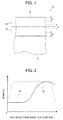
- FIG. 1 is a schematic view showing a gas barrier film 10 according to an embodiment of the present invention.
- the gas barrier film 10 is formed by depositing a silicon nitride layer 12 as gas barrier layer on a base film Z.
- the base film Z is not specifically limited and may be any of sheet materials of various kinds that allow the silicon nitride layer 12 to be deposited by plasma-enhanced CVD.
- the base film Z that may be advantageously used include plastic films (resin films) made of organic materials such as polyethylene terephthalate, polyethylene naphthalate (PEN), polyethylene, polypropylene, polystyrene, polyamide, polyvinyl chloride, polycarbonate, polyacrylonitrile, polyimide, polyacrylate, and polymethacrylate.
- plastic films made of organic materials such as polyethylene terephthalate, polyethylene naphthalate (PEN), polyethylene, polypropylene, polystyrene, polyamide, polyvinyl chloride, polycarbonate, polyacrylonitrile, polyimide, polyacrylate, and polymethacrylate.
- the base film Z to be used in the present invention may also be any of sheet materials formed of a base material such as any of those plastic films and a layer deposited thereon for imparting various functions, such as a protective layer, an adhesive layer, a light-reflecting layer, a light-shielding layer, a planarizing layer, a buffer layer, and a stress-relief layer.
- the base film Z may be a sheet material having a single layer formed on a base material or a sheet material having a plurality of layers deposited on a base material.
- the base film Z is a sheet material having a plurality of layers deposited on a base material, the same layer may be deposited in a plurality of layers or one or more layers may be silicon nitride layers that are deposited by the film deposition method (device) of the invention.
- the gas barrier film 10 has a silicon nitride layer 12 formed on the surface of the base film Z.
- the silicon nitride layer 12 comprises a low-density region 14 in a lower position closer to the base film Z deposited in the presence of a great proportion of SiH 3 radicals and a high density region 16 having a high density in an upper position closer to the top side opposite from the base film Z deposited in the presence of a great proportion of SiH 2 radicals.
- a lower region having a thickness of 20% indicated by arrow a in Fig. 1 has a mean density lower than the mean density of an upper region closer to the top side having a thickness of 20% indicated by arrow b, and a middle region having a thickness of 20% indicated by arrow c has a mean density between those of the lower and the upper regions a and b.
- the variation in composition in the film thickness direction may be measured by ESCA (Electron Spectroscopy for Chemical Analysis) to determine interfaces between adjacent layers where the N composition decreases and settles at a minimum and where the Si composition increases and settles at a maximum, and the interfaces thus determined may be used to detect the mean densities of the lower 20%-thickness layer, the upper 20%-thickness layer, and the middle 20%-thickness layer of the silicon nitride layer 12.
- ESCA Electron Spectroscopy for Chemical Analysis
- a typical silicon nitride layer is formed in the presence of a relatively great proportion of SiH 2 radicals in a middle region in the thickness direction whereas it is formed in the presence of a relatively great proportion of SiH 3 radicals in a top surface region and a lower region. Accordingly, the density of a typical silicon nitride layer is high in the middle region in the thickness direction and low in the top surface region and the lower region as conceptually shown by the dotted line in Fig. 2 .
- the middle region in the thickness direction has a substantially consistent density therein.
- the gas barrier film 10 of the invention has a composition such that, as indicated by the solid line in Fig. 2 , the low density region 14 in a lower position deposited in the presence of a great proportion of SiH 3 radicals and the high density region 16 having a high density in a position closer to the top surface deposited in the presence of a great proportion of SiH 2 radicals, the middle region between them having a density between those of the lower and upper positions.
- the present invention achieves production of the gas barrier film 10 excelling not only in productivity and gas barrier properties but oxidation resistance as well, with significantly reduced damage caused to the base film Z.
- the thickness of the silicon nitride layer 12 of the invention may be appropriately determined without any specific limitation according to such conditions as gas barrier properties and flexibility required of gas barrier films, applications for which the use of the film is intended, and the like, and is preferably 10 ⁇ m or more.
- the silicon nitride layer 12 preferably has a mean density of 1.7 to 2.1 [g/cm 3 ] in the 20%-thick lower region a and a mean density of 2.1 to 2.7 [g/cm 3 ] in the 20%-thick upper region b as shown in Fig. 1 .
- Fig. 3 schematically shows a film deposition device 20 for implementing a film deposition method to produce the gas barrier film 10 of the invention.
- the illustrated film deposition device 20 produces the gas barrier film 10 by depositing or forming the silicon nitride layer 12 by CCP (capacitively coupled plasma)-CVD on the surface of a long length of base film Z or a film material in the form of a web as it is transported in a longitudinal direction.
- CCP capactively coupled plasma
- the film deposition device 20 is a so-called roll-to-roll (R-to-R) type film deposition device whereby the base film Z is fed from a base film roll 24, a roll of elongated base film Z, the silicon nitride layer 12 is formed on the base film Z traveling in the longitudinal direction, and the base film Z having the silicon nitride layer 12 formed thereon, that is, the gas barrier film 10, is rewound into a roll.
- R-to-R roll-to-roll
- cut sheets cut to a given length may also be preferably used.
- the illustrated film deposition device 20 achieves deposition of the silicon nitride layer 12 by CCP-CVD
- the present invention is not limited this way.
- the invention permits use of various film deposition methods including ICP (Inductively Coupled Plasma)-CVD, microwave CVD, ECR (Electron Cyclotron Resonance), and atmospheric pressure plasma CVD, provided that the material gas flow is formed in the opposite direction to the base film transportation direction.
- ICP Inductively Coupled Plasma
- microwave CVD microwave CVD
- ECR Electro Cyclotron Resonance
- atmospheric pressure plasma CVD provided that the material gas flow is formed in the opposite direction to the base film transportation direction.
- illustrated CCP-CVD described later may be advantageously used as it uses shower head electrodes 46 having a plane opposite the base film Z to readily achieve formation of gas flow in film deposition region in the opposite direction to the base film transportation direction.
- the film deposition device 20 shown in Fig. 3 is a so-called roll-to-roll film deposition device whereby the base film Z is fed from the base film roll 24, which is a roll of elongated base film Z, and the silicon nitride layer 12 is formed on the base film Z traveling in the longitudinal direction before being rewound into a roll.
- the film deposition device 20 includes a feed chamber 26, a film deposition chamber 28 and a take-up chamber 30.
- the film deposition device 20 may also have various members of a roll-to-roll type device achieving film deposition by plasma CVD including various sensors, and various members (transport means) for transporting the base film Z along a predetermined path, as exemplified by a transport roller pair and a guide member for regulating the position in the width direction of the base film Z.
- the production device 10 may include a plurality of the same or different plasma CVD film deposition chambers.
- at least one film deposition chamber for depositing a film by any of other vapor deposition techniques than plasma-enhanced CVD, flash evaporation or sputtering and/or at least one surface treatment chamber for plasma treatment may be connected to the film deposition device.
- the feed chamber 26 includes a rotary shaft 32, a guide roller 34 and a vacuum evacuation means 36.
- the base film roll 24 into which a long length of base film Z is wound is mounted on the rotary shaft 32 in the feed chamber 26.
- the base film Z Upon mounting of the base film roll 24 on the rotary shaft 32, the base film Z travels along a predetermined travel path starting from the feed chamber 26 and passing through the film deposition chamber 28 to reach a take-up shaft 38 of the take-up chamber 30.
- Feeding of the base film Z from the base film roll 24 and winding of the base film Z on the take-up shaft 38 in the take-up chamber 30 are carried out in synchronism in the film deposition device 20 to continuously form the silicon nitride layer 12 on the elongated base film Z in the film deposition chamber 28 by CCP-CVD as the base film Z travels in its longitudinal direction along the predetermined travel path.
- the rotary shaft 32 is rotated by a drive source (not shown) in a clockwise direction in FIG. 1 so that the base film Z is fed from the base film roll 24, is guided by the guide roller 34 along the predetermined path and passes through a slit 40a provided in a partition wall 40 to reach the film deposition chamber 28.
- the feed chamber 26 and the take-up chamber 30 are provided with vacuum evacuation means 36 and 70, respectively.
- the vacuum evacuation means are provided in these chambers to ensure that these chambers have the same pressure (degree of vacuum) during film deposition as the film deposition chamber 28 described later so that the pressures inside these neighboring chambers do not affect the degree of vacuum inside the film deposition chamber 28 (deposition of the silicon nitride layer 12).
- the vacuum evacuation means 36 is not particularly limited, and exemplary means that may be used include vacuum pumps such as a turbo pump, a mechanical booster pump, a dry pump, and a rotary pump, an assist means such as a cryogenic coil, and various other known (vacuum) evacuation means which use a means for adjusting the ultimate degree of vacuum or the amount of air discharged and are employed in vacuum deposition devices.
- vacuum pumps such as a turbo pump, a mechanical booster pump, a dry pump, and a rotary pump
- an assist means such as a cryogenic coil
- various other known (vacuum) evacuation means which use a means for adjusting the ultimate degree of vacuum or the amount of air discharged and are employed in vacuum deposition devices.
- other vacuum evacuation means 59 and 70 various other known evacuation means which use a means for adjusting the ultimate degree of vacuum or the amount of air discharged and are employed in vacuum deposition devices.
- the base film Z is guided by the guide roller 34 to reach the film deposition chamber 28 through the slit 40a of the partition wall 40.
- the film deposition chamber 28 is provided to deposit or form the silicon nitride layer 12 on the surface of the base film Z by CCP-CVD.
- the film deposition chamber 28 includes a drum 42, a shower head electrode 46, guide rollers 48 and 50, a gas supply means 52, an RF power source 54, a bias current source 56, a gas stop means 58, and the vacuum evacuation means 59.
- the drum 42 in the film deposition chamber 28 is a cylindrical member rotating counterclockwise about the central axis in Fig. 1 , and the base film Z guided by the guide roller 48 along the predetermined path is passed over a predetermined region of the peripheral surface to travel onward in the longitudinal direction as the base film Z is held in a given position facing the shower head electrode 46 to be described later.
- the drum 42 also serves as a counter electrode in CCP-CVD and forms a pair of electrodes with the shower head electrode 46.
- the drum 42 is connected with the bias current source 56.
- the bias current source 56 may be any of various known current sources used as bias current source for CCP-CVD such as a 400 kHz RF current source.
- the present invention is not limited this way, however.
- the drum 42 may be connected to ground or may be selectively connected to ground and the bias power source 56.
- the illustrated example comprises the RF power source 54 for supplying plasma excitation current to the shower head electrode 46 described later
- the present invention is not limited this way.
- the RF power source 54 for supplying plasma excitation current may be connected to the drum 42, with the shower head electrode 46 connected to ground, to achieve film deposition by so-called self-bias type CCP-CVD.
- the drum 42 may be connected with the RF power source 54, with the shower head electrode 46 connected to the bias power source 56.
- the drum 42 may be connected to the RF power source 54, with the shower head electrode 46 selectively connected to the bias power source 56 or ground.
- drum 42 preferably comprises a temperature adjusting means.
- the temperature adjusting means of the drum 42 is not particularly limited and various types of temperature adjusting means may be used including one containing a refrigerant or a heating agent circulating in the drum and a cooling means using a piezoelectric element.
- the shower head electrode 46 is of a known type used in film deposition by means of CCP-CVD.
- the shower head electrode 46 is, by way of example, hollow and has a substantially rectangular shape, with one external plane thereof being inwardly curved into a shape forming a part of the inner periphery of a cylinder having a radius greater than that of the drum 42.
- the shower head electrode 46 is so disposed that the rotation axis of the drum 42 and the central axis of the curved plane coincide to keep the curved plane away from the opposite periphery of the drum 42 by the same distance throughout the curved plane. In other words, the difference in radius between them corresponds to the distance separating them, so that the gap between them remains constant.
- the curved plane of the shower head electrode 46 has numerous through-holes for emitting a material gas evenly distributed in the whole area of a region that has at least a chance of facing the base film Z.
- the shower head electrode 46 has a length in the drum axial direction (i.e., the direction normal to the base film transporting direction, which will also be referred to below as "width-wise" direction) exceeding a maximum width of the base film Z and preferably slightly exceeding the size of the drum 42 in the width direction.
- the shower head electrode 46 may comprise a wall-like shield member at its upstream end for preventing emission of a material gas from the gap between the upstream end of the shower head electrode 46 and the drum 42.
- the shower head electrode 46 according to the invention is not limited to the illustrated type having the curved plane and may be hollow and have a rectangular shape (hollow plate member) or may have a curved shape not parallel to the periphery of the drum.
- the present invention allows any of known shower head electrodes used in CCP-CVD.
- one shower head electrode (film deposition means using CCP-CVD) is provided in the film deposition chamber 28.
- the present invention is not limited to this configuration and a plurality of shower head electrodes may be disposed in the base film transport direction.
- the present invention is not limited to a configuration using the shower head electrode and allows a configuration comprising nozzles or the like for supplying a material gas provided between an electrode without the material gas emission holes (material gas supply means) and the other electrode to achieve CCP-CVD.
- the gas supply means 52 is of a known type used in vacuum deposition devices such as plasma CVD devices, and supplies a material gas (process gas) into the shower head electrode 46.
- the film deposition device 20 (film deposition method) of the invention uses material gas containing a gas forproducing silane radicals (SiH 3 and SiH 4 ) to achieve deposition of the silicon nitride layer 12.
- Preferred gases for producing silane radicals may be selected from various silane gases.
- Examples of such gases include silane [SiH 4 ], monomethyl silane [MMS CH 3 SiH 3 ], dimethyl silane [DMS (CH 3 ) 2 SiH 2 )], trimethyl silane [(C H 3) 3 SiH] , tetramethyl silane [TMS (CH 3 ) 4 Si], tetraethoxysilane [TEOS (C 2 H 5 O) 4 Si], triethoxysilane [TRIES (C 2 H 5 O) 3 SiH], methyl triethoxysilane [(C 2 H 5 O) 3 SiCH 3 ], dimethyl diethoxysilane [(C 2 H 5 O) 2 Si(CH 3 ) 2 ], tetramethoxysilane [(CH 3 O) 4 Si], diethyl silane [(C 2 H) 2 SiH 2 ] , triethyl silane [(C 2 H 5 ) 3 SiH], diethoxymethyl silane [(C 2 H 5 O) 2 SiH(CH 3 )
- the gas supply means 52 feed a material gas containing one or more of these gases to the shower head electrode 46.
- the material gas that may be any of various gases as appropriate including a known gas used for deposition of a silicon nitride layer using gas that produces the above-mentioned silane radicals and a combination of gases.
- the material gas examples include a combination of silane gas, ammonia gas, and hydrogen gas; a combination of silane gas, ammonia gas, nitrogen gas, and hydrogen gas; a combination of silane gas and ammonia gas; a combination of silane gas and nitrogen gas; and any of these combinations to which helium or argon is added as diluent gas.
- the RF power source 54 is one for supplying plasma excitation power to the shower head electrode 46.
- Known RF power sources used in various plasma CVD devices can be all used for the RF power source 54 including a power source that supplies 13.56 MHz RF electricity.
- the present invention permits use of various configurations in addition to one where the shower head electrode 46 is supplied with plasma excitation current, one example thereof being a self bias type where the drum 42 is supplied with plasma excitation current while the shower head electrode 46 is connected to ground.
- the vacuum evacuation means 59 evacuates the film deposition chamber 14 to keep it at a predetermined film deposition pressure for deposition of the silicon nitride layer 12 by plasma-enhanced CVD, and is of a known type used in vacuum deposition devices as described above.
- the film deposition chamber 28 comprises the gas shield means 58 adjacent a downstream end of the shower head electrode 46 in the base film transport direction.
- the downstream in the base film transport direction is also referred to simply as downstream, and the opposite stream as upstream.
- the gas shield means 58 is a sheet member disposed with an end thereof as close to the drum 42 and a plane thereof as close to the downstream end of the shower head electrode 46 as the configuration permits, as schematically illustrated in Fig. 4A by way of example.
- the gas shield means 58 has a width-wise length longer than the shorter of the width-wise sizes of the drum 42 and the shower head electrode 46.
- the gas shield means 58 may be disposed in contact with the shower head electrode 46.
- the gas shield means 58 may be provided in the shower head electrode 46.
- the gas blocking means 58 substantially closes the gap between the shower head electrode 46 and the drum 42 at the downstream end of the shower head electrode 46 to prevent the material gas from discharging from this position.
- the film deposition chamber 28 equipped with the gas blocking means 58 allows a gas flow of the material gas (also referred to below simply as material gas flow) to be created in the direction indicated by arrow b, which is the opposite direction to the base film transport direction (direction in which the drum 42 turns) indicated by arrow a in Fig. 4 , in the film deposition region, which is the region where the shower head electrode 46 and the drum 42 face each other in the illustrated example.
- material gas also referred to below simply as material gas flow
- the silicon nitride layer 12 is deposited on the surface of the base film by plasma-enhanced CVD as the base film Z is transported while the material gas flow is formed in the opposite direction to the base film transport direction, as described above.
- the present invention enables production of the gas barrier film 10 of the invention having the silicon nitride layer 12 deposited thereon comprising the lower low-density region 14 and the upper high-density region closer to the top surface and causing minimized damage to the base film Z, enabling a high productivity, and excelling in gas barrier properties and oxidation resistance with a single deposition means.
- the gas barrier film 10 of the invention can be produced with a pair of electrodes consisting of a gas material supply means and another electrode.
- silane radicals which reacts with nitrogen radicals (nitrogen containing radicals) produced from other material gases to form a silicon nitride layer.
- the silane radicals thus produced are primarily SiH 2 radials and SiH 3 radials. According to a study by the present inventors, a silicon nitride layer produced in the presence of SiH 2 radicals existing in a great proportion in the silicon nitride layer deposition process accompanied by production of silane radicals has a high density and excels in gas barrier properties and oxidation resistance.
- a silicon nitride layer produced in the presence of SiH 3 radicals existing in a great proportion in the silicon nitride layer deposition process accompanied by production of silane radicals excels in base film coverage (step coverage) capability and can adequately coat the base film surface even when the surface has significant irregularities, although the density is not so high compared with the above film. That is, the thickness of the layer for eliminating the adverse effects of the irregularities of the base film surface can be reduced, resulting in improved productivity.
- SiH 3 radicals produced by plasma only cause extremely small damage to the base film surface as compared with SiH 2 radicals.
- Fig. 5 shows base film coverage characteristics for comparison between film deposition in the presence of SiH 3 radicals existing in a great proportion (SiH 3 rich conditions) and film deposition in the presence of SiH 2 radicals existing in a great proportion (SiH 2 rich conditions).
- a trench base film as illustrated in Fig. 5A having corrugations each measuring 200 nm in width and 300 nm in height (depth).
- a silicon nitride layer was deposited on the trench base film under SiH 3 rich conditions and SiH 2 rich conditions to evaluate the base film coverage characteristics based on a ratio of the thickness of the film deposited on the lateral and bottom surfaces of the corrugations to the thickness of the film deposited on the top surface of the corrugations as conceptually illustrated in Fig. 5B .
- the material gas used was silane gas, ammonia gas, nitrogen gas and hydrogen. The electric current and gas flow rate were adjusted to provide SiH 3 rich and SiH 2 rich conditions.
- Fig. 5C show that the film deposited under SiH 3 -rich conditions has a thickness on both the lateral and bottom surfaces that are closer to the thickness thereof on the top surface as compared with the film deposited under SiH 2 -rich conditions and excels the film deposited under SiH 2 -rich conditions in base film coverage characteristics.
- the gas barrier film 10 of the invention which comprises the silicon nitride layer 12 causing significantly reduced damage to the base film Z and excelling in not only productivity but gas barrier properties and oxidation resistance, with a lower low-density region 14 and a high-density region 16 closer to the top surface can be produced by first carrying out film deposition in the presence of SiH 3 radicals existing in a great proportion, followed by film deposition in the presence of SiH 2 radicals existing in a great proportion.
- SiH 2 radicals are consumed by film deposition earlier than SiH 3 radicals.
- SiH 2 radicals change into SiH 3 radicals as they hit other radicals or as time passes.
- the material gas is used for deposition of the silicon nitride layer under conditions where SiH 3 radicals exist in a great proportion on the upstream side (in the starting stage of film deposition, in the lower position of the layer, i.e., in a position closer to the base film), and the proportion of SiH 3 radicals decreases toward the downstream side whereas the proportion of SiH 2 radicals gradually increases, so that the material gas is used for deposition of the silicon nitride layer under conditions where SiH 2 radicals exist in a great proportion on the downstream side (in the terminating stage of film deposition, in a position closer to the top surface).
- the present invention enables production, with a single deposition means using plasma-enhanced CVD, of the gas barrier film 10 of the invention having the silicon nitride layer 12 deposited thereon comprising the lower low-density region 14 and the upper high-density region closer to the top surface, with a density distribution such that the middle region having a mean density between those of the low-density region and the high-density region as shown by the solid line in Fig. 2 and having excellent properties described above.
- the gas barrier film 10 of the invention can be produced with a pair of electrodes consisting of a gas material supply means and another electrode.
- the production method of the invention achieves production of the gas barrier film 10 of the invention aiming at simplification of the device, reduction in size of the device, cost reduction, and the like. Further, the configuration needing only one film deposition means allows the film deposition means to be of larger dimensions than with a configuration requiring a plurality of film deposition means, thus enabling improvement on productivity.
- the shower head electrode 46 is of a known type used in film deposition by means of CCP-CVD.
- a typical shower head electrode 46 of this kind is so designed as to allow a material gas to reach the whole area of the film deposition region evenly. To that end, the material gas is allowed to flow both upstream and downstream from the center of the shower head electrode 46 with respect to the transport direction in film deposition by typical CCP-CVD that does not use the gas shield member 58. As a result, SiH 2 radicals exist in a greater proportion near the center whereas SiH 3 radicals exist in a greater proportion in regions close to the upstream and downstream ends. However, because the shower head electrode 46 supplies the material gas evenly throughout the whole film deposition region, the material gas flow is slow, and the difference in proportion in which both radicals exist in respective film deposition regions in the base film transport direction is not considerably great.
- the silicon nitride layer produced by typical CCP-CVD has a high and uniform density in the middle region and a low density at both ends as indicated by the dotted line in Fig. 2 .
- the method of forming the material gas flow in the opposite direction to the base film transport direction according to the invention is not limited to the method illustrated in Fig. 4A and may be any of various methods as appropriate depending on the configuration of the film deposition device.
- a wall member 60a or the like may be provided in addition to the gas blocking means 58 to provide a gas discharge passage 60 for guiding material gas that was not used for reaction to an appropriate position.
- a suction means 62 such as a suction fan for sucking the material gas may be provided in a position along the gas discharge passage 60 or close to the outlet thereof).
- the material gas flow may be alternatively created by means of the gas discharge passage 60 and the suction means 62 without using the gas blocking means 58.
- the suction means 62 may be the only means used to cause the material gas flow.
- the shower head electrode may have such a configuration wherein gas emission holes are provided downstream with a high density and upstream with a lower density than downstream so as to make a difference between upstream and downstream in the amount of introduced material gas thereby to create a material gas flow in the opposite direction to the transport direction (direction a) as in the shower head electrode 46a as illustrated in Fig. 4C in lieu of the shower head electrode 46 where the material gas emission holes are evenly distributed along the film deposition region.
- the density of the emission holes may gradually decrease from downstream to upstream or the gas emission holes may be provided in a given upstream region, a given downstream region, and other regions of the shower head electrode with the densities decreasing from the downstream region through said other region to the upstream region.
- the gas emission holes may be provided only in a given downstream region.
- the inside of the shower head electrode may be divided into regions, and the amounts of material gas supplied to these divided regions may be so adjusted as to make a difference in the amount of introduced material gas between upstream and downstream thereby to produce the material gas flow in the opposite direction to the transport direction.
- the film deposition conditions such as the material gas supply amount and the magnitude of the plasma excitation current are not specifically limited.
- the film deposition conditions may be determined as appropriate according to required film deposition speed, final film thickness, the kind of base film Z, and the like as in silicon nitride layer deposition using typical plasma-enhanced CVD.
- a certain level of plasma excitation power is required, preferably it is in a range of 1 W/cm 2 to 8 W/cm 2 .
- the material gas flow rate is also not specifically limited and may be determined as appropriate by conducting experiments and simulations under conditions according to the base film transport speed, required gas barrier film properties, and the like.
- the difference in density between the low-density region 14 and the high-density region 16 can be adjusted by changing, for example, the material gas flow rate, base film Z transport speed, the length of the film deposition region (along the transport direction of the shower head electrode), supplied electric power, and the like.
- the base film Z guided by the guide roller 48 is passed over the peripheral surface of the drum 42 and held in a given position as it is transported along the longitudinal direction.
- plasma is excited as the shower head electrode 46 is supplied with plasma excitation power, whereupon the material gas yields radicals, and the silicon nitride layer 12 is deposited by CCP-CVD on the surface of the base film Z that, supported by the drum 42 and transported further onward.
- the base film Z having the silicon nitride layer 12 deposited thereon (i.e., gas barrier film 10) is then guided by the guide roller 50 and transported through the slit 64a of the partition wall 64 to enter the take up chamber 30.
- the take-up chamber 30 includes the guide roller 68, the take-up shaft 38 and the vacuum evacuation means 70.
- the base film Z (gas barrier film) having reached the take-up chamber 30 travels to the take-up shaft 38 as it is guided by the guide roller 58 and is wound on the take-up shaft 38 to form a roll, which is then supplied to the subsequent step as a roll of gas barrier film.
- the take-up chamber 30 is also provided with the vacuum evacuation means 70 as in the above-described feed chamber 26 and during film deposition, its pressure is reduced to a degree of vacuum suitable for the film deposition pressure in the film deposition chamber 28.
- the base film Z Upon mounting of the base film roll 24 on the rotary shaft 32, the base film Z follows a given transport path as it is reeled out from the base film roll 24, travels from the feed chamber 26, and is guided by the guide roller 34 to reach the film deposition chamber 28, where the base film Z is guided by the guide roller 48, passed over a predetermined region of the peripheral surface of the drum 42 and guided by the guide roller 50 to reach the take-up chamber 30, where the base film Z is guided by a guide roller 68 to reach the take-up shaft 38.
- the vacuum evacuation means 36, 59, and 70 are actuated to reduce the chambers to their given pressures.
- the gas supply means 52 supplies the shower head electrode 46 with the material gas in the film deposition chamber 28.
- the base film Z starts to be transported from the feed chamber 26 toward the take-up chamber 30 while the RF power source 54 starts to supply the shower head electrode 46 with plasma excitation power and, optionally, the bias current source 56 starts to supply the drum 42 with bias current.
- the base film Z transported from the feed chamber 26 to the film deposition chamber 28 is guided by the guide roller 48 and transported onward as it is passed over the drum 42 while the silicon nitride layer 12 is deposited by CCP-CVD in the region where the drum 42 and the shower head electrode 46 face.
- the film deposition chamber 26 comprises the gas shield means 58 at the downstream end of the shower head electrode 46 in the base film transport direction to prevent material gas discharge from the gap between the drum 42 and the shower head electrode 46.
- the material gas is caused to flow in the opposite direction to the transport direction, so that the silicon nitride layer 12 deposited comprises, as described above, the lower low-density region 14 and the upper high-density region closer to the top surface and exhibits a density distribution as indicated by the solid line in Fig. 2 .
- the base film Z having the silicon nitride layer 12 deposited thereon, i.e., gas barrier film 10, is then guided by the guide roller 50 and transported to the take-up chamber 30.
- the base film Z having reached the take-up chamber 30 is guided by the guide roller 68 along a given path and rewound by the take-up shaft 30 into a roll, which is then supplied to the subsequent step as the gas barrier film 10.
- the film deposition device 20 as illustrated in Fig. 3 was used to deposit a silicon nitride layer on the base film Z to produce a gas barrier film.
- the base film Z used was a 100 ⁇ m-thick PEN film provided by Teijin DuPont Films Japan Limited.
- the material gas used included silane gas (SiH 4 ), ammonia gas (NH 3 ), and hydrogen gas (H2).
- the supply amounts of silane gas, ammonia gas, and hydrogen gas were 200 sccm, 500 sccm, and 1200 sccm, respectively.
- the shower head electrode 46 was supplied with plasma excitation power having a frequency of 13.5 MHz and an output of 2W/cm 2 .
- the drum 42 was adjusted to a temperature of 40°C and supplied with a bias current having a frequency of 400 kHz and an output of 600 W.
- the film deposition pressure was 20 Pa; the base film transport speed was 1 m/min.
- the silicon nitride layer with a thickness of 50 nm was deposited on the surface of the base film Z to produce the gas barrier film 10.
- the produced gas barrier film was measured by Rutherford backscattering/hydrogen forward scattering analysis (RBS/HFS) to determine the mean densities in the lower 20%-thickness region closer to the base film (indicated by arrow a in Fig. 1 ), the upper 20%-thickness region closer to the top surface (indicated by arrow b in Fig. 1 ), and the middle 20%-thickness region between them (indicated by arrow c in Fig. 1 ) of the silicon nitride layer 12.
- RRS/HFS Rutherford backscattering/hydrogen forward scattering analysis
- the mean densities in the lower region, the upper region, and the middle region were 1.9 [g/cm 3 ], 2.3 [g/cm 3 ], and 2.1 [g/cm 3 ], respectively.
- a gas barrier film was produced in the same manner as in Working Example 1 except that the shower head electrode 46 was connected to ground and not supplied with plasma excitation power whereas the drum 42 was supplied with plasma excitation power having a frequency of 13.5 MHz and an output of 2W/cm 2 (self-bias configuration).
- the thickness of the silicon nitride layer 12 was 50 nm, which was the same as that in Working Example 1.
- the travel speed of the base film Z was set to 2 m/min.
- the mean densities in the respective regions were measured in the same manner as in Working Example 1: the mean densities in the lower region, the top surface region, and the middle region were 2.0 [g/cm 3 ], 2.4 [g/cm 3 ] and 2.2 [g/cm 3 ], respectively.
- a gas barrier film was produced in the same manner as in Working Example 1 except that the gas shield member 58 was not provided.
- the thickness of the silicon nitride layer 12 was 50 nm, which was the same as that in Working Example 1.
- the mean densities in the respective regions were measured in the same manner as in Working Example 1: the mean densities in the lower region, the top surface region, and the middle region were 2.3 [g/cm 3 ], 2.3 [g/cm 3 ], and 2.3 [g/cm 3 ], respectively.
- the gas barrier films thus produced were evaluated for base film coverage properties, gas barrier properties, damage to the base film, and oxidation resistance of the silicon nitride layer.
- the trench base film illustrated in Fig. 5A was attached to the drum 42 and film deposition was carried out in the same manner as in Working Examples 1 and 2 and Comparative Example 1 to examine the base film coverage properties.
- the base film coverage properties were evaluated based on a ratio of the thickness of the film deposited on the bottom surface of the corrugations to the thickness of the film deposited on the top surface of the corrugations as in the case illustrated in Fig. 5C . Ratings were given as follows.
- the moisture vapor transmission rate [g/(m 2 ⁇ day)] was measured by the MOCON method.
- the surface of the produced gas barrier films were scanned by an atomic force microscope (AFM) covering an area of 10 ⁇ m x 10 ⁇ m and their arithmetic mean roughness (Ra) was calculated to determine the damage conditions of the base film. Ratings were given as follows.
- the gas barrier film was subjected to a storage test in an environment of 85°C and 85%RH for 1000 hours.
- the composition of the layer before and after the storage was examined by X-ray photoelectron spectroscopy (abbreviated as XPS; Quantera SXM available from Ulvac-Phi, Incorporated) to evaluate the oxidation resistance of the film.
- XPS X-ray photoelectron spectroscopy
- Quantera SXM available from Ulvac-Phi, Incorporated
- Table 1 Mean density [g/cm 3 ] Coverage properties Gas barrier properties Minimized damage to base film Oxidation resistance lower middle upper Working Example 1 1.9 2.1 2.3 Good ⁇ 1x10 -4 Excellent Excellent Working Example 2 2.0 2.2 2.4 Excellent ⁇ 1x10 -4 Good Excellent Comparative Example 1 2.3 2.3 2.3 Poor >1x10 -3 Poor Poor
- the gas barrier film of the invention produced by the production device (method) according to the invention excels the comparative examples produced by conventional methods in all of base film coverage properties, gas barrier properties, minimizing of damage to the base film, and oxidation resistance.
- the present invention may be advantageously applied to gas barrier films used in various displays such as liquid crystal displays, solar cells, and the like and to production of these gas barrier films.
Landscapes
- Chemical & Material Sciences (AREA)
- Engineering & Computer Science (AREA)
- Metallurgy (AREA)
- Chemical Kinetics & Catalysis (AREA)
- Materials Engineering (AREA)
- Mechanical Engineering (AREA)
- Organic Chemistry (AREA)
- General Chemical & Material Sciences (AREA)
- Physics & Mathematics (AREA)
- Plasma & Fusion (AREA)
- Inorganic Chemistry (AREA)
- Chemical Vapour Deposition (AREA)
- Laminated Bodies (AREA)
Applications Claiming Priority (1)
| Application Number | Priority Date | Filing Date | Title |
|---|---|---|---|
| JP2010047633A JP5463168B2 (ja) | 2010-03-04 | 2010-03-04 | 成膜方法および成膜装置 |
Publications (3)
| Publication Number | Publication Date |
|---|---|
| EP2363511A2 true EP2363511A2 (de) | 2011-09-07 |
| EP2363511A3 EP2363511A3 (de) | 2011-10-19 |
| EP2363511B1 EP2363511B1 (de) | 2017-04-26 |
Family
ID=44063274
Family Applications (1)
| Application Number | Title | Priority Date | Filing Date |
|---|---|---|---|
| EP11154967.1A Not-in-force EP2363511B1 (de) | 2010-03-04 | 2011-02-18 | Filmabscheidungsverfahren und Filmabscheidungsvorrichtung |
Country Status (4)
| Country | Link |
|---|---|
| US (1) | US20110217533A1 (de) |
| EP (1) | EP2363511B1 (de) |
| JP (1) | JP5463168B2 (de) |
| CN (1) | CN102191478B (de) |
Cited By (3)
| Publication number | Priority date | Publication date | Assignee | Title |
|---|---|---|---|---|
| CN104395067A (zh) * | 2012-04-19 | 2015-03-04 | 住友化学株式会社 | 层叠膜 |
| WO2015067739A1 (en) | 2013-11-08 | 2015-05-14 | Nestec S.A. | Coated container |
| EP3093309A1 (de) | 2015-05-11 | 2016-11-16 | Coating Plasma Industrie | Verfahren zum aufbringen einer gassperrschicht auf eine polymerfolie oder einen polymerbehälter und polymerfolie oder polymerbehälter mit solch einer gassperre |
Families Citing this family (7)
| Publication number | Priority date | Publication date | Assignee | Title |
|---|---|---|---|---|
| TWI477642B (zh) * | 2012-07-25 | 2015-03-21 | E Ink Holdings Inc | 阻氣基板 |
| JP6019054B2 (ja) * | 2014-03-24 | 2016-11-02 | 富士フイルム株式会社 | ガスバリアフィルムおよびガスバリアフィルムの製造方法 |
| CN110431004A (zh) * | 2017-03-31 | 2019-11-08 | 富士胶片株式会社 | 阻气膜及成膜方法 |
| WO2019065020A1 (ja) * | 2017-09-27 | 2019-04-04 | 富士フイルム株式会社 | ガスバリアフィルム |
| EP4162094A4 (de) * | 2020-06-04 | 2024-10-02 | Applied Materials, Inc. | Dampfabscheidungsvorrichtung und verfahren zur beschichtung eines substrats in einer vakuumkammer |
| JP7811120B2 (ja) * | 2022-02-07 | 2026-02-04 | 富士フイルム株式会社 | 大気圧プラズマ処理方法および大気圧プラズマ処理装置 |
| CN115527903B (zh) * | 2022-11-24 | 2023-11-03 | 西安奕斯伟材料科技股份有限公司 | 一种用于背封硅片的设备和方法 |
Citations (3)
| Publication number | Priority date | Publication date | Assignee | Title |
|---|---|---|---|---|
| JP2002105649A (ja) | 2000-09-28 | 2002-04-10 | Toppan Printing Co Ltd | 真空成膜装置及び真空成膜方法 |
| JP2005283561A (ja) | 2004-03-04 | 2005-10-13 | Sumitomo Bakelite Co Ltd | 水蒸気透過度測定装置 |
| JP2009031612A (ja) | 2007-07-27 | 2009-02-12 | Ulvac Japan Ltd | 樹脂基板 |
Family Cites Families (14)
| Publication number | Priority date | Publication date | Assignee | Title |
|---|---|---|---|---|
| US4664951A (en) * | 1985-07-31 | 1987-05-12 | Energy Conversion Devices, Inc. | Method provided for corrective lateral displacement of a longitudinally moving web held in a planar configuration |
| JP3118037B2 (ja) * | 1991-10-28 | 2000-12-18 | キヤノン株式会社 | 堆積膜形成方法および堆積膜形成装置 |
| JPH07321200A (ja) * | 1994-05-20 | 1995-12-08 | Casio Comput Co Ltd | シリコン窒化膜の形成方法およびその膜を有する薄膜トラン ジスタ |
| JPH1129873A (ja) * | 1997-07-11 | 1999-02-02 | Sekisui Chem Co Ltd | 積層膜の形成方法及びその形成装置 |
| US8652625B2 (en) * | 2004-09-21 | 2014-02-18 | Konica Minolta Holdings, Inc. | Transparent gas barrier film |
| JP4646609B2 (ja) * | 2004-12-01 | 2011-03-09 | シャープ株式会社 | プラズマcvd装置 |
| US20090252893A1 (en) * | 2005-08-31 | 2009-10-08 | Koji Ozaki | Plasma discharge treatment apparatus, and method of manufacturing gas barrier film |
| US20100009147A1 (en) * | 2007-02-05 | 2010-01-14 | Kazuhiro Fukuda | Transparent gas barrier film |
| US8586189B2 (en) * | 2007-09-19 | 2013-11-19 | Fujifilm Corporation | Gas-barrier film and organic device comprising same |
| JP5084426B2 (ja) * | 2007-09-27 | 2012-11-28 | 富士フイルム株式会社 | 窒化シリコン膜の形成方法 |
| JP5081712B2 (ja) * | 2008-05-02 | 2012-11-28 | 富士フイルム株式会社 | 成膜装置 |
| JP2009280873A (ja) * | 2008-05-23 | 2009-12-03 | Fujifilm Corp | ガスバリアフィルムの製造方法 |
| KR101842675B1 (ko) * | 2009-07-08 | 2018-03-27 | 플라즈마시, 인크. | 플라즈마 처리를 위한 장치 및 방법 |
| JP5665290B2 (ja) * | 2009-08-24 | 2015-02-04 | 富士フイルム株式会社 | 成膜装置 |
-
2010
- 2010-03-04 JP JP2010047633A patent/JP5463168B2/ja active Active
-
2011
- 2011-02-18 EP EP11154967.1A patent/EP2363511B1/de not_active Not-in-force
- 2011-03-04 CN CN201110054321.6A patent/CN102191478B/zh not_active Expired - Fee Related
- 2011-03-04 US US13/040,853 patent/US20110217533A1/en not_active Abandoned
Patent Citations (3)
| Publication number | Priority date | Publication date | Assignee | Title |
|---|---|---|---|---|
| JP2002105649A (ja) | 2000-09-28 | 2002-04-10 | Toppan Printing Co Ltd | 真空成膜装置及び真空成膜方法 |
| JP2005283561A (ja) | 2004-03-04 | 2005-10-13 | Sumitomo Bakelite Co Ltd | 水蒸気透過度測定装置 |
| JP2009031612A (ja) | 2007-07-27 | 2009-02-12 | Ulvac Japan Ltd | 樹脂基板 |
Cited By (4)
| Publication number | Priority date | Publication date | Assignee | Title |
|---|---|---|---|---|
| CN104395067A (zh) * | 2012-04-19 | 2015-03-04 | 住友化学株式会社 | 层叠膜 |
| CN104395067B (zh) * | 2012-04-19 | 2016-11-09 | 住友化学株式会社 | 层叠膜 |
| WO2015067739A1 (en) | 2013-11-08 | 2015-05-14 | Nestec S.A. | Coated container |
| EP3093309A1 (de) | 2015-05-11 | 2016-11-16 | Coating Plasma Industrie | Verfahren zum aufbringen einer gassperrschicht auf eine polymerfolie oder einen polymerbehälter und polymerfolie oder polymerbehälter mit solch einer gassperre |
Also Published As
| Publication number | Publication date |
|---|---|
| JP5463168B2 (ja) | 2014-04-09 |
| CN102191478A (zh) | 2011-09-21 |
| EP2363511B1 (de) | 2017-04-26 |
| US20110217533A1 (en) | 2011-09-08 |
| JP2011184703A (ja) | 2011-09-22 |
| EP2363511A3 (de) | 2011-10-19 |
| CN102191478B (zh) | 2015-09-02 |
Similar Documents
| Publication | Publication Date | Title |
|---|---|---|
| EP2363511B1 (de) | Filmabscheidungsverfahren und Filmabscheidungsvorrichtung | |
| JP5136114B2 (ja) | ガスバリア膜の作製方法及び作製装置 | |
| US20100261008A1 (en) | Gas barrier film and method of producing the same | |
| CN102383107B (zh) | 薄膜沉积装置 | |
| US20110041765A1 (en) | Film deposition device | |
| EP2085495B1 (de) | Ablagerungsverfahren für eine Gassperrschicht | |
| JP4830733B2 (ja) | ガスバリアフィルムおよびその製造方法 | |
| EP2396451A1 (de) | Zweischichtige barriere auf polymersubstrat | |
| CN101189360B (zh) | 通过表面波等离子体形成蒸镀膜的方法及装置 | |
| EP2365105B1 (de) | Gassperrfolie, Verfahren und Vorrichtung zur Filmabscheidung | |
| US20090087586A1 (en) | Method of forming silicon nitride films | |
| US8273419B2 (en) | Method of forming gas barrier layers including a change in pressure, a gas barrier layer formed by the method, and a gas barrier film | |
| US11090917B2 (en) | Laminate and method for fabricating the same | |
| JP5319342B2 (ja) | ガスバリア膜の製造方法、太陽電池用ガスバリアフィルム、および、ディスプレイ用ガスバリアフィルム | |
| US8491971B2 (en) | Method of producing gas barrier layer | |
| TW201919890A (zh) | 積層膜 | |
| JP6593347B2 (ja) | ガスバリアフィルムの製造方法及び製造装置 | |
| WO2015163358A1 (ja) | ガスバリアーフィルム及びその製造方法 | |
| JP2018108643A (ja) | フィルム積層体、その製造方法及び成膜装置 | |
| JP2013209691A (ja) | 機能性フィルムの製造方法および製造装置 | |
| WO2017085984A1 (ja) | プラズマcvd成膜装置 |
Legal Events
| Date | Code | Title | Description |
|---|---|---|---|
| PUAI | Public reference made under article 153(3) epc to a published international application that has entered the european phase |
Free format text: ORIGINAL CODE: 0009012 |
|
| AK | Designated contracting states |
Kind code of ref document: A2 Designated state(s): AL AT BE BG CH CY CZ DE DK EE ES FI FR GB GR HR HU IE IS IT LI LT LU LV MC MK MT NL NO PL PT RO RS SE SI SK SM TR |
|
| AX | Request for extension of the european patent |
Extension state: BA ME |
|
| PUAL | Search report despatched |
Free format text: ORIGINAL CODE: 0009013 |
|
| AK | Designated contracting states |
Kind code of ref document: A3 Designated state(s): AL AT BE BG CH CY CZ DE DK EE ES FI FR GB GR HR HU IE IS IT LI LT LU LV MC MK MT NL NO PL PT RO RS SE SI SK SM TR |
|
| AX | Request for extension of the european patent |
Extension state: BA ME |
|
| RIC1 | Information provided on ipc code assigned before grant |
Ipc: C23C 16/509 20060101ALI20110915BHEP Ipc: C23C 16/54 20060101ALI20110915BHEP Ipc: C23C 16/52 20060101ALI20110915BHEP Ipc: C23C 16/455 20060101ALI20110915BHEP Ipc: C23C 30/00 20060101ALI20110915BHEP Ipc: C23C 16/34 20060101AFI20110915BHEP |
|
| 17P | Request for examination filed |
Effective date: 20120330 |
|
| 17Q | First examination report despatched |
Effective date: 20151009 |
|
| GRAP | Despatch of communication of intention to grant a patent |
Free format text: ORIGINAL CODE: EPIDOSNIGR1 |
|
| INTG | Intention to grant announced |
Effective date: 20161201 |
|
| GRAS | Grant fee paid |
Free format text: ORIGINAL CODE: EPIDOSNIGR3 |
|
| GRAA | (expected) grant |
Free format text: ORIGINAL CODE: 0009210 |
|
| AK | Designated contracting states |
Kind code of ref document: B1 Designated state(s): AL AT BE BG CH CY CZ DE DK EE ES FI FR GB GR HR HU IE IS IT LI LT LU LV MC MK MT NL NO PL PT RO RS SE SI SK SM TR |
|
| REG | Reference to a national code |
Ref country code: GB Ref legal event code: FG4D |
|
| RIN1 | Information on inventor provided before grant (corrected) |
Inventor name: NISHIDA, HIROYUKI |
|
| REG | Reference to a national code |
Ref country code: CH Ref legal event code: EP |
|
| REG | Reference to a national code |
Ref country code: AT Ref legal event code: REF Ref document number: 887957 Country of ref document: AT Kind code of ref document: T Effective date: 20170515 |
|
| REG | Reference to a national code |
Ref country code: IE Ref legal event code: FG4D |
|
| REG | Reference to a national code |
Ref country code: DE Ref legal event code: R096 Ref document number: 602011037278 Country of ref document: DE |
|
| REG | Reference to a national code |
Ref country code: NL Ref legal event code: MP Effective date: 20170426 |
|
| REG | Reference to a national code |
Ref country code: LT Ref legal event code: MG4D |
|
| REG | Reference to a national code |
Ref country code: AT Ref legal event code: MK05 Ref document number: 887957 Country of ref document: AT Kind code of ref document: T Effective date: 20170426 |
|
| PG25 | Lapsed in a contracting state [announced via postgrant information from national office to epo] |
Ref country code: NL Free format text: LAPSE BECAUSE OF FAILURE TO SUBMIT A TRANSLATION OF THE DESCRIPTION OR TO PAY THE FEE WITHIN THE PRESCRIBED TIME-LIMIT Effective date: 20170426 |
|
| PG25 | Lapsed in a contracting state [announced via postgrant information from national office to epo] |
Ref country code: GR Free format text: LAPSE BECAUSE OF FAILURE TO SUBMIT A TRANSLATION OF THE DESCRIPTION OR TO PAY THE FEE WITHIN THE PRESCRIBED TIME-LIMIT Effective date: 20170727 Ref country code: LT Free format text: LAPSE BECAUSE OF FAILURE TO SUBMIT A TRANSLATION OF THE DESCRIPTION OR TO PAY THE FEE WITHIN THE PRESCRIBED TIME-LIMIT Effective date: 20170426 Ref country code: HR Free format text: LAPSE BECAUSE OF FAILURE TO SUBMIT A TRANSLATION OF THE DESCRIPTION OR TO PAY THE FEE WITHIN THE PRESCRIBED TIME-LIMIT Effective date: 20170426 Ref country code: NO Free format text: LAPSE BECAUSE OF FAILURE TO SUBMIT A TRANSLATION OF THE DESCRIPTION OR TO PAY THE FEE WITHIN THE PRESCRIBED TIME-LIMIT Effective date: 20170726 Ref country code: FI Free format text: LAPSE BECAUSE OF FAILURE TO SUBMIT A TRANSLATION OF THE DESCRIPTION OR TO PAY THE FEE WITHIN THE PRESCRIBED TIME-LIMIT Effective date: 20170426 Ref country code: AT Free format text: LAPSE BECAUSE OF FAILURE TO SUBMIT A TRANSLATION OF THE DESCRIPTION OR TO PAY THE FEE WITHIN THE PRESCRIBED TIME-LIMIT Effective date: 20170426 Ref country code: ES Free format text: LAPSE BECAUSE OF FAILURE TO SUBMIT A TRANSLATION OF THE DESCRIPTION OR TO PAY THE FEE WITHIN THE PRESCRIBED TIME-LIMIT Effective date: 20170426 |
|
| PG25 | Lapsed in a contracting state [announced via postgrant information from national office to epo] |
Ref country code: IS Free format text: LAPSE BECAUSE OF FAILURE TO SUBMIT A TRANSLATION OF THE DESCRIPTION OR TO PAY THE FEE WITHIN THE PRESCRIBED TIME-LIMIT Effective date: 20170826 Ref country code: RS Free format text: LAPSE BECAUSE OF FAILURE TO SUBMIT A TRANSLATION OF THE DESCRIPTION OR TO PAY THE FEE WITHIN THE PRESCRIBED TIME-LIMIT Effective date: 20170426 Ref country code: PL Free format text: LAPSE BECAUSE OF FAILURE TO SUBMIT A TRANSLATION OF THE DESCRIPTION OR TO PAY THE FEE WITHIN THE PRESCRIBED TIME-LIMIT Effective date: 20170426 Ref country code: SE Free format text: LAPSE BECAUSE OF FAILURE TO SUBMIT A TRANSLATION OF THE DESCRIPTION OR TO PAY THE FEE WITHIN THE PRESCRIBED TIME-LIMIT Effective date: 20170426 Ref country code: LV Free format text: LAPSE BECAUSE OF FAILURE TO SUBMIT A TRANSLATION OF THE DESCRIPTION OR TO PAY THE FEE WITHIN THE PRESCRIBED TIME-LIMIT Effective date: 20170426 Ref country code: BG Free format text: LAPSE BECAUSE OF FAILURE TO SUBMIT A TRANSLATION OF THE DESCRIPTION OR TO PAY THE FEE WITHIN THE PRESCRIBED TIME-LIMIT Effective date: 20170726 |
|
| REG | Reference to a national code |
Ref country code: DE Ref legal event code: R097 Ref document number: 602011037278 Country of ref document: DE |
|
| PG25 | Lapsed in a contracting state [announced via postgrant information from national office to epo] |
Ref country code: RO Free format text: LAPSE BECAUSE OF FAILURE TO SUBMIT A TRANSLATION OF THE DESCRIPTION OR TO PAY THE FEE WITHIN THE PRESCRIBED TIME-LIMIT Effective date: 20170426 Ref country code: SK Free format text: LAPSE BECAUSE OF FAILURE TO SUBMIT A TRANSLATION OF THE DESCRIPTION OR TO PAY THE FEE WITHIN THE PRESCRIBED TIME-LIMIT Effective date: 20170426 Ref country code: EE Free format text: LAPSE BECAUSE OF FAILURE TO SUBMIT A TRANSLATION OF THE DESCRIPTION OR TO PAY THE FEE WITHIN THE PRESCRIBED TIME-LIMIT Effective date: 20170426 Ref country code: DK Free format text: LAPSE BECAUSE OF FAILURE TO SUBMIT A TRANSLATION OF THE DESCRIPTION OR TO PAY THE FEE WITHIN THE PRESCRIBED TIME-LIMIT Effective date: 20170426 Ref country code: CZ Free format text: LAPSE BECAUSE OF FAILURE TO SUBMIT A TRANSLATION OF THE DESCRIPTION OR TO PAY THE FEE WITHIN THE PRESCRIBED TIME-LIMIT Effective date: 20170426 |
|
| PG25 | Lapsed in a contracting state [announced via postgrant information from national office to epo] |
Ref country code: SM Free format text: LAPSE BECAUSE OF FAILURE TO SUBMIT A TRANSLATION OF THE DESCRIPTION OR TO PAY THE FEE WITHIN THE PRESCRIBED TIME-LIMIT Effective date: 20170426 Ref country code: IT Free format text: LAPSE BECAUSE OF FAILURE TO SUBMIT A TRANSLATION OF THE DESCRIPTION OR TO PAY THE FEE WITHIN THE PRESCRIBED TIME-LIMIT Effective date: 20170426 |
|
| PLBE | No opposition filed within time limit |
Free format text: ORIGINAL CODE: 0009261 |
|
| STAA | Information on the status of an ep patent application or granted ep patent |
Free format text: STATUS: NO OPPOSITION FILED WITHIN TIME LIMIT |
|
| 26N | No opposition filed |
Effective date: 20180129 |
|
| PG25 | Lapsed in a contracting state [announced via postgrant information from national office to epo] |
Ref country code: SI Free format text: LAPSE BECAUSE OF FAILURE TO SUBMIT A TRANSLATION OF THE DESCRIPTION OR TO PAY THE FEE WITHIN THE PRESCRIBED TIME-LIMIT Effective date: 20170426 |
|
| REG | Reference to a national code |
Ref country code: CH Ref legal event code: PL |
|
| PG25 | Lapsed in a contracting state [announced via postgrant information from national office to epo] |
Ref country code: MC Free format text: LAPSE BECAUSE OF FAILURE TO SUBMIT A TRANSLATION OF THE DESCRIPTION OR TO PAY THE FEE WITHIN THE PRESCRIBED TIME-LIMIT Effective date: 20170426 |
|
| REG | Reference to a national code |
Ref country code: IE Ref legal event code: MM4A |
|
| REG | Reference to a national code |
Ref country code: BE Ref legal event code: MM Effective date: 20180228 |
|
| PG25 | Lapsed in a contracting state [announced via postgrant information from national office to epo] |
Ref country code: LI Free format text: LAPSE BECAUSE OF NON-PAYMENT OF DUE FEES Effective date: 20180228 Ref country code: LU Free format text: LAPSE BECAUSE OF NON-PAYMENT OF DUE FEES Effective date: 20180218 Ref country code: CH Free format text: LAPSE BECAUSE OF NON-PAYMENT OF DUE FEES Effective date: 20180228 |
|
| REG | Reference to a national code |
Ref country code: FR Ref legal event code: ST Effective date: 20181031 |
|
| PG25 | Lapsed in a contracting state [announced via postgrant information from national office to epo] |
Ref country code: IE Free format text: LAPSE BECAUSE OF NON-PAYMENT OF DUE FEES Effective date: 20180218 |
|
| PG25 | Lapsed in a contracting state [announced via postgrant information from national office to epo] |
Ref country code: BE Free format text: LAPSE BECAUSE OF NON-PAYMENT OF DUE FEES Effective date: 20180228 Ref country code: FR Free format text: LAPSE BECAUSE OF NON-PAYMENT OF DUE FEES Effective date: 20180228 |
|
| PG25 | Lapsed in a contracting state [announced via postgrant information from national office to epo] |
Ref country code: MT Free format text: LAPSE BECAUSE OF NON-PAYMENT OF DUE FEES Effective date: 20180218 |
|
| PG25 | Lapsed in a contracting state [announced via postgrant information from national office to epo] |
Ref country code: TR Free format text: LAPSE BECAUSE OF FAILURE TO SUBMIT A TRANSLATION OF THE DESCRIPTION OR TO PAY THE FEE WITHIN THE PRESCRIBED TIME-LIMIT Effective date: 20170426 |
|
| PG25 | Lapsed in a contracting state [announced via postgrant information from national office to epo] |
Ref country code: PT Free format text: LAPSE BECAUSE OF FAILURE TO SUBMIT A TRANSLATION OF THE DESCRIPTION OR TO PAY THE FEE WITHIN THE PRESCRIBED TIME-LIMIT Effective date: 20170426 Ref country code: HU Free format text: LAPSE BECAUSE OF FAILURE TO SUBMIT A TRANSLATION OF THE DESCRIPTION OR TO PAY THE FEE WITHIN THE PRESCRIBED TIME-LIMIT; INVALID AB INITIO Effective date: 20110218 |
|
| PG25 | Lapsed in a contracting state [announced via postgrant information from national office to epo] |
Ref country code: MK Free format text: LAPSE BECAUSE OF NON-PAYMENT OF DUE FEES Effective date: 20170426 Ref country code: CY Free format text: LAPSE BECAUSE OF FAILURE TO SUBMIT A TRANSLATION OF THE DESCRIPTION OR TO PAY THE FEE WITHIN THE PRESCRIBED TIME-LIMIT Effective date: 20170426 |
|
| PG25 | Lapsed in a contracting state [announced via postgrant information from national office to epo] |
Ref country code: AL Free format text: LAPSE BECAUSE OF FAILURE TO SUBMIT A TRANSLATION OF THE DESCRIPTION OR TO PAY THE FEE WITHIN THE PRESCRIBED TIME-LIMIT Effective date: 20170426 |
|
| PGFP | Annual fee paid to national office [announced via postgrant information from national office to epo] |
Ref country code: DE Payment date: 20210202 Year of fee payment: 11 Ref country code: GB Payment date: 20210210 Year of fee payment: 11 |
|
| REG | Reference to a national code |
Ref country code: DE Ref legal event code: R119 Ref document number: 602011037278 Country of ref document: DE |
|
| GBPC | Gb: european patent ceased through non-payment of renewal fee |
Effective date: 20220218 |
|
| PG25 | Lapsed in a contracting state [announced via postgrant information from national office to epo] |
Ref country code: GB Free format text: LAPSE BECAUSE OF NON-PAYMENT OF DUE FEES Effective date: 20220218 Ref country code: DE Free format text: LAPSE BECAUSE OF NON-PAYMENT OF DUE FEES Effective date: 20220901 |