EP2365363A2 - Fotoelektrischer Wandler - Google Patents
Fotoelektrischer Wandler Download PDFInfo
- Publication number
- EP2365363A2 EP2365363A2 EP11004806A EP11004806A EP2365363A2 EP 2365363 A2 EP2365363 A2 EP 2365363A2 EP 11004806 A EP11004806 A EP 11004806A EP 11004806 A EP11004806 A EP 11004806A EP 2365363 A2 EP2365363 A2 EP 2365363A2
- Authority
- EP
- European Patent Office
- Prior art keywords
- substrate
- mount substrate
- light emitting
- photoelectric converter
- waveguide
- Prior art date
- Legal status (The legal status is an assumption and is not a legal conclusion. Google has not performed a legal analysis and makes no representation as to the accuracy of the status listed.)
- Granted
Links
Images














Classifications
-
- G—PHYSICS
- G02—OPTICS
- G02B—OPTICAL ELEMENTS, SYSTEMS OR APPARATUS
- G02B6/00—Light guides; Structural details of arrangements comprising light guides and other optical elements, e.g. couplings
- G02B6/24—Coupling light guides
- G02B6/42—Coupling light guides with opto-electronic elements
-
- G—PHYSICS
- G02—OPTICS
- G02B—OPTICAL ELEMENTS, SYSTEMS OR APPARATUS
- G02B6/00—Light guides; Structural details of arrangements comprising light guides and other optical elements, e.g. couplings
- G02B6/24—Coupling light guides
- G02B6/42—Coupling light guides with opto-electronic elements
- G02B6/4201—Packages, e.g. shape, construction, internal or external details
- G02B6/4204—Packages, e.g. shape, construction, internal or external details the coupling comprising intermediate optical elements, e.g. lenses, holograms
- G02B6/4214—Packages, e.g. shape, construction, internal or external details the coupling comprising intermediate optical elements, e.g. lenses, holograms the intermediate optical element having redirecting reflective means, e.g. mirrors, prisms for deflecting the radiation from horizontal to down- or upward direction toward a device
-
- G—PHYSICS
- G02—OPTICS
- G02B—OPTICAL ELEMENTS, SYSTEMS OR APPARATUS
- G02B6/00—Light guides; Structural details of arrangements comprising light guides and other optical elements, e.g. couplings
- G02B6/10—Light guides; Structural details of arrangements comprising light guides and other optical elements, e.g. couplings of the optical waveguide type
-
- G—PHYSICS
- G02—OPTICS
- G02B—OPTICAL ELEMENTS, SYSTEMS OR APPARATUS
- G02B6/00—Light guides; Structural details of arrangements comprising light guides and other optical elements, e.g. couplings
- G02B6/24—Coupling light guides
- G02B6/42—Coupling light guides with opto-electronic elements
- G02B6/4201—Packages, e.g. shape, construction, internal or external details
-
- G—PHYSICS
- G02—OPTICS
- G02B—OPTICAL ELEMENTS, SYSTEMS OR APPARATUS
- G02B6/00—Light guides; Structural details of arrangements comprising light guides and other optical elements, e.g. couplings
- G02B6/24—Coupling light guides
- G02B6/42—Coupling light guides with opto-electronic elements
- G02B6/4201—Packages, e.g. shape, construction, internal or external details
- G02B6/4219—Mechanical fixtures for holding or positioning the elements relative to each other in the couplings; Alignment methods for the elements, e.g. measuring or observing methods especially used therefor
- G02B6/4228—Passive alignment, i.e. without a detection of the degree of coupling or the position of the elements
- G02B6/4232—Passive alignment, i.e. without a detection of the degree of coupling or the position of the elements using the surface tension of fluid solder to align the elements, e.g. solder bump techniques
-
- G—PHYSICS
- G02—OPTICS
- G02B—OPTICAL ELEMENTS, SYSTEMS OR APPARATUS
- G02B6/00—Light guides; Structural details of arrangements comprising light guides and other optical elements, e.g. couplings
- G02B6/24—Coupling light guides
- G02B6/42—Coupling light guides with opto-electronic elements
- G02B6/4201—Packages, e.g. shape, construction, internal or external details
- G02B6/4274—Electrical aspects
- G02B6/4284—Electrical aspects of optical modules with disconnectable electrical connectors
-
- H—ELECTRICITY
- H10—SEMICONDUCTOR DEVICES; ELECTRIC SOLID-STATE DEVICES NOT OTHERWISE PROVIDED FOR
- H10W—GENERIC PACKAGES, INTERCONNECTIONS, CONNECTORS OR OTHER CONSTRUCTIONAL DETAILS OF DEVICES COVERED BY CLASS H10
- H10W90/00—Package configurations
- H10W90/20—Configurations of stacked chips
- H10W90/293—Configurations of stacked chips characterised by non-galvanic coupling between the chips, e.g. capacitive coupling
-
- G—PHYSICS
- G02—OPTICS
- G02B—OPTICAL ELEMENTS, SYSTEMS OR APPARATUS
- G02B6/00—Light guides; Structural details of arrangements comprising light guides and other optical elements, e.g. couplings
- G02B6/10—Light guides; Structural details of arrangements comprising light guides and other optical elements, e.g. couplings of the optical waveguide type
- G02B6/12—Light guides; Structural details of arrangements comprising light guides and other optical elements, e.g. couplings of the optical waveguide type of the integrated circuit kind
- G02B2006/12133—Functions
- G02B2006/12147—Coupler
-
- G—PHYSICS
- G02—OPTICS
- G02B—OPTICAL ELEMENTS, SYSTEMS OR APPARATUS
- G02B6/00—Light guides; Structural details of arrangements comprising light guides and other optical elements, e.g. couplings
- G02B6/24—Coupling light guides
- G02B6/42—Coupling light guides with opto-electronic elements
- G02B6/43—Arrangements comprising a plurality of opto-electronic elements and associated optical interconnections
-
- H—ELECTRICITY
- H10—SEMICONDUCTOR DEVICES; ELECTRIC SOLID-STATE DEVICES NOT OTHERWISE PROVIDED FOR
- H10W—GENERIC PACKAGES, INTERCONNECTIONS, CONNECTORS OR OTHER CONSTRUCTIONAL DETAILS OF DEVICES COVERED BY CLASS H10
- H10W90/00—Package configurations
- H10W90/701—Package configurations characterised by the relative positions of pads or connectors relative to package parts
- H10W90/721—Package configurations characterised by the relative positions of pads or connectors relative to package parts of bump connectors
- H10W90/724—Package configurations characterised by the relative positions of pads or connectors relative to package parts of bump connectors between a chip and a stacked insulating package substrate, interposer or RDL
Definitions
- the present invention relates to a photoelectric converter provided with an optical element.
- a photoelectric converter as described in, for example, Fig. 9 of Patent Document 1, there is known a type including: a light emitting element which emits light by converting an electric signal into an optical signal; a substrate on which an IC circuit for transmitting an electric signal to the light emitting element is formed and the light emitting element is mounted on one surface from the side opposite to the light emitting side of the light emitting element: and a waveguide which is arranged to extend from the light emitting element in the direction perpendicular to the one surface of the substrate and transmits the light emitted by the light emitting element.
- a light receiving element which receives light and converts the received optical signal to an electric signal.
- a male electric connector which is attachable and detachable to and from a female electric connector provided on a wiring substrate, is provided on the other surface of the substrate, and the substrate and the wiring substrate are electrically connected to each other by connecting these electric connectors.
- a waveguide is provided so as to extend from the light emitting element in the direction perpendicular to the one surface of the substrate, which causes the height of the whole device to be significantly increased.
- the light emitting direction of the light emitting element is adapted to be arranged in parallel with the wiring substrate by providing the electric connector on the side surface of the substrate.
- the device height at least corresponding to the size of the light emitting element and a control IC element is necessary, and hence it is not possible to significantly suppress the device height.
- Patent Document 1 Japanese Patent Laid-Open No. 2001-42170
- an object of the present invention is to provide a photoelectric converter which makes it possible to reduce the device height.
- a photoelectric converter characterized by including: a mount substrate; an IC circuit adapted to be provided on the mount substrate; an optical element adapted to have a function of converting an electric signal output from the IC circuit to an optical signal and emitting light, or a function of converting a received optical signal to an electric signal and outputting the electric signal to the IC circuit; and a waveguide adapted to effect an optical coupling between the optical element and an external optical device, and in that the optical element is held on the mount substrate and has a light emitting surface or a light receiving surface, the light emitting surface or the light receiving surface being directed to the mount substrate, and the waveguide is provided on the mount substrate along the surface of the mount substrate.
- the waveguide is provided along the surface of the mount substrate, it is possible to suppress the height of the whole device in the thickness direction of the mount substrate, and to thereby achieve the low height of the device.
- Fig. 1 shows a photoelectric converter 1A according to a first embodiment of the present invention.
- the photoelectric converter 1A includes a light emitting side photoelectric converting portion (also referred to as E/O module) 1A1 adapted to be mounted on a wiring substrate 2 by engagement of a header (electric connector) 6 and a socket (electric connector) 7, a light receiving side photoelectric converting portion (also referred to as O/E module) 1A2 adapted to be mounted by engagement of the electric connectors 6 and 7 similarly to the other wiring substrate 2, and an external waveguide 9 adapted to effect an optical coupling between the converting portions 1A1 and 1A2. That is, in the photoelectric converter 1A, the electric converting portion on the other side seen from the light emitting side photoelectric converting portion 1A1 or the light receiving side photoelectric converting portion 1A2 is positioned as an "external optical device".
- E/O module light emitting side photoelectric converting portion
- O/E module light receiving side photoelectric converting portion
- the vertical direction in Fig. 1 means the vertical direction
- the direction perpendicular to the paper surface in Fig. 1 means the right and left direction
- the right side and the left side in Fig. 1 means the front and the rear for the light emitting side photoelectric converting portion 1A1, respectively
- the left side and the right side in Fig. 1 means the front and the rear for the light receiving side photoelectric converting portion 1A2.
- the light emitting side photoelectric converting portion 1A1 is provided with a mount substrate 3 formed into a rectangular form extending in the front and rear direction in plan view. As shown in Fig. 2 , a light emitting element 4A which converts an electric signal to an optical signal and emits light, and an IC substrate 5A in which an IC circuit 50A for transmitting the electric signal to the light emitting element 4A is formed, are mounted on one surface 3a set as the lower surface of the mount substrate 3.
- the header type electric connector (hereinafter referred to simply as a "header") 6 is provided so as to cover these components 4A and 5A from below.
- a mirror portion 33 which converts an optical path of a light beam emitted by the light emitting element 4A by approximately 90 degrees is provided at a position just above the light emitting element 4A, and an internal waveguide 31 optically coupled with the light emitting element 4A is provided so as to extend from the mirror portion 33 to the front end surface 3b of the mount substrate 3.
- the light emitting element 4A emits light upward from the upper surface, and is mounted on the one surface 3a of the mount substrate 3 from the light emitting side.
- a VCSEL Very Cavity Surface Emitting Laser
- the IC substrate 5A is a driver IC for driving the VCSEL, and arranged near the light emitting element 4A.
- the light emitting element 4A and the IC substrate 5A are connected to the wiring pattern 36 of the mount substrate 3 by bumps 11 (see Fig. 3 ) made of gold or solder.
- an LED or the like can also be adopted as the light emitting element 4A.
- the LED or the like has no directivity and a small optical coupling rate with the internal waveguide 31, and hence can be adopted under the condition that there is a margin in the efficiency of light. In such case, the LED or the like is advantageous in terms of low cost.
- the mount substrate 3 is preferably formed of a material having a coefficient of linear thermal expansion close to that of the light emitting element 4A, and may be formed of a compound semiconductor such as GaAs which is the same material system as the VCSEL material, except silicon.
- the mount substrate 3 may also be formed of a ceramics material, such as aluminum nitride and silicon nitride, as a material having an excellent coefficient of linear expansion and thermal conductivity.
- the mirror portion 33 can be formed by making gold and aluminum vapor-deposited on the 45-degree inclined surface which is formed by etching the mount substrate 3.
- the 45-degree inclined surface can be formed by, for example, an anisotropic etching using a potassium hydroxide solution.
- the internal waveguide 31 is provided along the one surface 3a of the mount substrate 3, and adapted to transmit the light emitted by the light emitting element 4A in the direction parallel to the one surface 3a of the mount substrate 3.
- the internal waveguide 31 is constituted by two kinds of resin having different refractive indices.
- the internal waveguide 31 is constituted by a core 31a for guiding light and a clad 31b which covers and holds the core 31a from the circumference thereof, as shown in Fig. 3 , and is provided in a groove 32 for waveguide formation which is formed in the mount substrate 3.
- the core 31a is made of resin having a high refractive index
- clad 31b is made of resin having a low refractive index.
- the size of the core 31a and the clad 31b is determined by the calculation of the optical loss due to the divergent angle of the light emitting element 4A, the light receiving diameter of the light receiving element 4B, as will be described below, and the like.
- the internal waveguide 31 may be constituted by an inorganic material such as quartz other than resin, provided that the material is a light transmissive material.
- the external waveguide 9 is adapted to be joined to the front end surface 3b of the mount substrate 3 by an optical adhesive, so that the internal waveguide 31 is optically coupled with the external waveguide 9 by the joining processing. That is, the waveguide according to the present invention is constituted by the mirror portion 33, the internal waveguide 31, and the external waveguide 9. Note that when the distance from the mirror portion 33 to the external waveguide 9 is short, there is a case where the amount of the loss caused by simply making the light propagated in the air is small. In this case, the light may be made directly incident on the external waveguide 9 from the mirror portion 33 by eliminating the internal waveguide 31.
- the film-like external waveguide 9 is superior in bending characteristics, and hence there is no problem even when it is used in, for example, a bending portion of a cellular phone (cell phone, mobile phone) or the like.
- light loss may be caused depending on the bending curvature, it is possible to reduce the light loss by increasing the difference in refractive index between the core and the clad.
- a quartz based fiber or a plastic fiber may also be used other than the film-like waveguide.
- the front end surface 3b of the mount substrate 3 and the external waveguide 9 are joined to each other in such a manner that a gap between the mount substrate 3 and the external waveguide 9 is set to 5 to 30 ⁇ m, and an adhesive is filled in the gap so as to be cured by ultraviolet rays.
- it is possible to fill the adhesive without any shortage of the adhesive by filling the adhesive in the gap between the mount substrate 3 and the external waveguide 9 at the time when the gap is set to about 100 ⁇ m, and then reducing the gap.
- the groove 32 for waveguide formation is formed in the mount substrate 3, it is possible to simplify the positioning between the mount substrate 3 and the external waveguide 9 and to realize passive alignment, by forming a groove in the other portion, and also providing in the external waveguide 9 a portion shaped so as to be engaged with the groove.
- the header 6 is a type which can be attached and detached to and from the socket type electric connector (hereinafter referred to simply as "socket") 7 which is an external connector provided on the wiring substrate 2.
- the header 6 and the socket 7 are replaceable with each other. It may be adapted such that the socket 7 is provided on the mount substrate 3, and the header 6 is provided on the wiring substrate 2 to make the header 6 serve as an external connector.
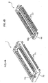
- the socket 7 is formed into substantially a rectangular form extending in the front and rear direction in plan view, as shown in Fig. 4A .
- the socket 7 has a socket body 72 and a terminal 71 held by the socket body 72.
- a rectangular frame-like fitting recess 72a is provided in the socket body 72 in plan view, and the terminal 71 is exposed in the fitting recess 72a.
- the end of the terminal 71 extends from the socket body 72 in the left and right directions, and is connected to a wiring pattern (not shown) formed on the upper surface of the wiring substrate 2, by solder (not shown) or the like.
- the socket 7 is usually mounted on the wiring substrate 2 by reflow soldering.
- the header 6 is formed into substantially a rectangular form which is one size smaller than the socket 7 and extends in the front and rear direction in bottom view, as shown in Fig. 4B .
- the header 6 has a header body 62 and a terminal 61 held by the header body 62.
- a rectangular frame-like fitting protrusion 62a fittable to the fitting recess 72a of the socket 7 is formed in the header body 62 in bottom view, and the terminal 61 is exposed on the surface of the fitting protrusion 62a.
- the end of the terminal 61 extends from the header body 62 in the left and right directions, and is connected to the wiring pattern 36 of the mount substrate 3 by solder balls 10.
- a terminal post, a pin or the like besides the solder ball. Note that the height including the mount substrate 3 and the solder ball 10 is about 1 mm.
- the terminals 61 and 71 are brought into contact with each other so that the wiring pattern of the wiring substrate 2 is electrically connected to the wiring pattern 36 of the mount substrate 3.
- the height from the lower surface of the socket 7 to the upper surface of the header 6 is about 1 mm.
- the height from the upper surface of the wiring substrate 2 to the other surface 3c of the mount substrate 3 is about 2 mm.
- the fundamental constitution of the light receiving side photoelectric converting portion 1A2 is the same as that of the light emitting side photoelectric converting portion 1A1, and detailed explanation thereof is omitted.
- the light receiving side photoelectric converting portion 1A2 is different from the light emitting side photoelectric converting portion 1A1 in that a light receiving element 4B which receives light and converts the optical signal to an electric signal, and an IC substrate 5B in which an IC circuit 50B for receiving the electric signal from the light receiving element 4B is formed, are mounted on the one surface 3a of the mount substrate 3, as shown in Fig. 5 .
- a PD photodiode
- the IC substrate 5B is a TIA (Transimpedance Amplifier) element which performs current/voltage conversion. Further, an amplifier element may also be mounted on the mount substrate 3.
- TIA Transimpedance Amplifier
- the light emitting side photoelectric converting portion 1A1 and the light receiving side photoelectric converting portion 1A2 can be separately manufactured and the manufacturing methods for these are the same.
- the manufacturing method of light emitting side photoelectric converting portion 1A1 is explained on behalf of the methods.
- the external waveguide 9 is joined to the light emitting side photoelectric converting portion 1A1 and the light receiving side photoelectric converting portion 1A2 which are manufactured in this way, so that the light emitting side photoelectric converting portion 1A1 and the light receiving side photoelectric converting portion 1A2 are optically connected to each other.
- the header 6 is provided on the one surface 3a of the mount substrate 3 on which the light emitting element 4A or the light receiving element 4B is mounted, while the waveguide is constituted by the mirror portion 33, the internal waveguide 31 and the external waveguide 9, and the internal waveguide 31 is provided along the one surface 3a of the mount substrate 3.
- the waveguide is constituted by the mirror portion 33, the internal waveguide 31 and the external waveguide 9, and the internal waveguide 31 is provided along the one surface 3a of the mount substrate 3.
- the mount substrate 3 is a silicon substrate, and hence the mirror portion 33 and the internal waveguide 31 can be easily formed.
- the photoelectric converter 1A there is shown a one-way communication type in which an optical signal is sent from the light emitting side photoelectric converting portion 1A1 to the light receiving side photoelectric converting portion 1A2, but the photoelectric converter 1A may be a two-way communication type in which a light receiving element 4B is mounted in the light emitting side photoelectric converting portion 1A1, a light emitting element 4A is mounted in the light receiving side photoelectric converting portion 1A2, and a plurality of waveguides 31 are formed in the mount substrate 3. Further, the photoelectric converter 1A may be provided with an external waveguide 9 and at least one of the light emitting side photoelectric converting portion 1A1 and the light receiving side photoelectric converting portion 1A2.
- the photoelectric converter 1A may be a multi-channel communication type in which array type light emitting and receiving elements are mounted, and a plurality of wave guides may also be formed so as to be used as the external waveguide 9.
- the photoelectric converter 1A of the first embodiment various modifications are possible for the photoelectric converter 1A of the first embodiment.
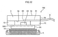
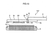
- modified example 1 to modified example 5 of the photoelectric converter 1A are explained with reference to Fig. 9 to Fig. 13 .
- the light receiving side photoelectric converting portion is also the same as the light emitting side photoelectric converting portion, and hence only the light emitting side photoelectric converting portion is illustrated and explained.
- the mount substrate 3 is arranged so that the one surface 3a on which the light emitting element 4A is mounted is set as the upper surface, and a through-electrode 37 which electrically connects a wiring pattern (not shown) formed on the one surface 3a to the wiring pattern (not shown) formed on the other surface 3c, is provided in the mount substrate 3.
- the IC substrate 5A is mounted, and the header 6 is provided.
- the mount substrate 3 is arranged so as to set the one surface 3a as the upper surface, and the through-electrodes 37 are provided in the mount substrate 3.
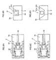
- the IC circuit 50A for transmitting an electric signal to the light emitting element 4A is directly formed, and the header 6 is provided.
- the function of the IC substrate 5A is provided for the mount substrate 3. This makes it possible to miniaturize the device.
- the IC circuit 50A is not necessarily formed on the other surface 3c, and may also be formed on the one surface 3a as shown in Fig. 10B .
- the mount substrate 3 may be arranged so that the one surface 3a, on which the light emitting element 4A is mounted and the IC circuit 50A is formed, is set as the lower surface, and the header 6 is formed on the one surface 3a. This makes the through-electrode 37 unnecessary.
- the light emitting element 4A is mounted on the IC substrate 5A, and the IC substrate 5A is mounted on the one surface 3a of the mount substrate 3. That is, the light emitting element 4A is mounted on the one surface 3a of the mount substrate 3 via the IC substrate 5A. Specifically, the light emitting element 4A is mounted on the IC substrate 5A by the die bonding and the wire bonding. Further, the IC substrate 5A is connected to the wiring pattern (not shown) formed on the one surface 3a of the mount substrate 3 by solder bumps 12 in order to secure a predetermined gap between the IC substrate 5A and the mount substrates 3. The header 6 is mounted on the one surface 3a of the mount substrate 3 with somewhat larger solder balls 10, in order to secure a somewhat larger gap between the header 6 and the mount substrates 3.
- the IC substrate 5A can be mounted on the mount substrate 3 after the light emitting element 4A is mounted on the IC substrate 5A, so that alignment of the light emitting element 4A with respect to the mirror portion 33 can be performed afterwards.
- a recessed portion 38 for preventing interference with the light emitting element 4A may be provided in the mount substrate 3, so that the waveguide 31 is formed on the bottom surface of the recessed portion 38.
- resin structural portions 13 are formed at both the front and rear ends of the one surface 3a of the mount substrate 3, and the IC substrate 5A on which the light emitting element 4A is mounted is mounted on the mount substrate 3 via the resin structural portions 13.
- the header 6 is mounted on the lower surface of the IC substrate 5A with the solder balls 10, and the header 6 is provided on the one surface 3a of the mount substrate 3 via the IC substrate 5A and the resin structural portions 13.
- a through hole 34 is provided at a position corresponding to the light emitting element 4A on the mount substrate 3, and an optically transmissive resin is filled in the through hole 34 so that an auxiliary waveguide 35 is formed.
- the header 6 is provided on the one surface 3a of the mount substrate 3, and the external waveguide 9 is joined to the other surface 3c of the mount substrate 3.
- the external waveguide 9 is provided along the other surface 3c by being joined to the other surface 3c of the mount substrate 3. Further, the end of the external waveguide 9 is arranged just above the waveguide 35, and a mirror surface 91 is formed at the end by cutting the end at an angle of 45 degrees.
- the light emitted from the light emitting element 4A enters into the external waveguide 9 through the waveguide 35, and is transmitted by the external waveguide 9 after the optical path of the light is converted by the mirror surface 91 by 90 degrees. That is, in modified example 5, the waveguide according to the present invention is constituted only by the external waveguide 9.
- the mount substrate 3 when the mount substrate 3 is arranged so as to cover the light emitting element 4A as shown in Fig. 1 , Fig. 10C , Fig. 11 , Fig. 12 and Fig. 13 , the mount substrate 3 serves as the ground to provide an effect of suppressing the noise.
- a photoelectric converter 1B according to a second embodiment of the present invention is explained with reference to Fig. 14 to Fig. 17 .
- the light receiving side photoelectric converting portion is the same as the light emitting side photoelectric converting portion, and hence only the light emitting side photoelectric converting portion is illustrated and explained.
- components which are the same as those of the first embodiment are denoted by the same reference numerals and characters, and the explanation thereof is omitted.
- the header 6 is provided on the wiring substrate 2, and the socket 7 is provided on the mount substrate 3 of a light emitting side photoelectric converting portion 1B1.
- a rectangular recessed portion 72b extending in the front and rear direction in bottom view is provided in a part surrounded by the fitting recess 72a, and the terminal 71 is exposed on the bottom surface of the recessed portion 72b.
- the mount substrate 3 is arranged so that the one surface 3a on which the light emitting element 4A is mounted is set as the upper surface.
- the bottom surface of the recessed portion 72b is joined to the one surface 3a of the mount substrate 3 by connecting the terminal 71 exposed on the bottom surface of the recessed portion 72b to the circuit pattern (not shown) formed on the one surface 3a of the mount substrate 3 with the solder balls 10.
- the socket 7 may be provided on the wiring substrate 2, so that the header 6 is provided on the mount substrate 3 of the light emitting side photoelectric converting portion 1B1.
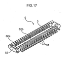
- the terminal 61 may be exposed on the bottom surface of a recessed portion 62b which is formed by being surrounded by the fitting protrusions 62a of the header body 62 of the header 6, and the terminal 61 may be connected to the wiring pattern (not shown) of the one surface 3a of the mount substrate 3 with the solder balls 10.
- the recessed portion 72b is provided in the socket body 72 of the socket 7 in order to avoid the interference with the mount substrate 3.
- a photoelectric converter 1C according to a third embodiment of the present invention is shown in Fig. 18 .
- an interposer substrate (wiring substrate) 8 is interposed between the one surface 3a of the mount substrate 3 and the header 6. That is, the upper surface of the interposer substrate 8 is connected to the one surface 3a of the mount substrate 3 with solder balls 15, and the header 6 is connected to the lower surface of the interposer substrate 8 with the solder balls 10.
- the interposer substrate 8 is constituted by a multilayer board, in such a manner that as shown in Fig. 19 , electrodes are formed on the uppermost layer 81 in correspondence with the wiring pattern (not shown) formed on the one surface 3a of the mount substrate 3, and electrodes are formed on the lowermost layer 83 in correspondence with the terminals 61 of the header 6, and that by electrically connecting the electrodes on the uppermost layer and the electrodes on the lowermost layer by an intermediate layer 82, the electrode pitch is converted and thereby the electrode pattern is changed.
- the number of electrodes on the uppermost layer 81 and the number of electrodes on the lowermost layer 83 are not necessarily adapted to correspond to one to one in the interposer substrate 8, and it is also possible to make the electrodes on the uppermost layer 81 collected into one and electrically connected to the electrodes of the lowermost layer 83. Therefore, it is also possible to reduce the number of terminals of the header 6 and the socket 7 by collecting the electric lines by using the interposer substrate 8.
- the interposer substrate 8 is particularly effective.
- the mount substrate 3 in a state where the one surface 3a is set as the upper surface, the mount substrate 3 may be arranged so that the interposer substrate 8 is interposed between the other surface 3c of the mount substrate 3 and the header 6. Further, it is also possible to apply modified example 2 to modified example 5 which are shown in the first embodiment.
- the header 6 and the socket 7 are replaceable with each other. This is the same as in third to fifth embodiments as will be described below.
- the interposer substrate 8 is not necessarily interposed between the mount substrate 3 and the header 6.
- the header 6 and the mount substrate 3 may be arranged side by side, and mounted on the interposer substrate 8 so that the interposer substrate 8 is arranged to extend over the header 6 and the mount substrate 3.
- the whole size is increased but the dimension in the thickness direction is reduced, which is effective for mobile devices, such as a cellular phone which has a limitation in the thickness direction.
- a photoelectric converter 1D according to a fourth embodiment of the present invention is shown in Fig. 21 .
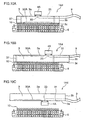
- a flexible electric circuit film 14 is stuck on the lower surface of the external waveguide 9.
- the electric circuit film 14 is adapted to hold, by an insulating material, conductive lines 14a for transmitting power from the light emitting side photoelectric converting portion 1D1 to the light receiving side photoelectric converting portion (not shown), or for receiving power by the light emitting side photoelectric converting portion 1D1 from the light receiving side photoelectric converting portion. Note that it is possible to transmit or receive not only power but also various signals by the conductive lines 14a.
- the whole length of the electric circuit film 14 is set longer than the length of the external waveguide 9, so that both ends 141 of the electric circuit film 14 extend from the external waveguide 9 in the front and rear direction. Also, it is adapted such that when the external waveguide 9 is joined to the front end surface 3b of the mount substrate 3, the end 141 of the electric circuit film 14 overlaps the one surface 3a of the mount substrate 3.
- the end 141 of the electric circuit film 14 is connected to the header 6, and the conductive lines 14a are directly connected to the header 6. Specifically, the conductive lines 14a are connected to the terminal 61 of the header 6 with the solder balls 10. Note that a conductor such as a copper post can also be used for this connection, besides the solder ball 10.
- the conductive lines 14a are directly connected to the header 6, which makes it possible to perform the electric connection for electric signals and the electric connection for power transmission or reception by the single header 6.
- a photoelectric converter 1E according to a fifth embodiment of the present invention is shown in Fig. 23 .
- the photoelectric converter 1E of the fifth embodiment has substantially the same constitution as that of the photoelectric converter 1C of the third embodiment, but is different from the photoelectric converter 1C in that the interposer substrate 8 of the light emitting side photoelectric converting portion 1E1 is extended in the direction in which the external waveguide 9 is extended, so as to be integrated with the interposer substrate 8 of the light receiving side photoelectric converting portion (not shown).
- the interposer substrate 8 may be constituted as a freely bendable flexible wiring film, or constituted in such a manner that a portion interposed between the header 6 and the mount substrate 3 is constituted by a substrate having a strength, and the flexible film is connected to the end surface of the interposed portion.
- an electric circuit for transmitting power from the light emitting side photoelectric converting portion 1E1 to the light receiving side photoelectric converting portion or for receiving power by the light emitting side photoelectric converting portion 1E1 from the light receiving side photoelectric converting portion. Note that the electric circuit is capable of transmitting or receiving not only power but also various signals.
- the interposer substrate 8 is adapted to be a flexible substrate, and hence the interposer substrate 8 can be bent together with the external waveguide 9. Also, only a gap corresponding to the solder ball 15 is provided between the external waveguide 9 and the interposer substrate 8. Thus, the external waveguide 9 and the interposer substrate 8 can be superposed and handled like the same film, without deteriorating the handling property. Further, these are independently provided, so that it is possible to obtain an excellent bending property.
- a plurality of light emitting elements 4A (eight in the figure), each of which emits a light beam of a different wavelength, are mounted side by side in the right and left direction on the one surface 3a of the mount substrate 3, and the width of the internal waveguide 31 is increased by increasing the groove width of the groove 32 for waveguide formation.
- the cross sectional shape of the groove 32 for waveguide formation has substantially a trapezoidal shape similar to that explained with reference to Fig. 8C and Fig. 8D .
- a plurality of incident portions 311 each of which is optically coupled to each of the light emitting elements 4A and an emitting portion 312 connected to the incident portions 311 are provided in the internal waveguide 31.
- a plurality of branches 313 are provided for the core 31a of the internal waveguide 31, so as to make the core 31 successively branched from the emitting side toward the incident side, that is to say, from the front end surface 3b side of the mount substrate 3 toward the rear.
- the light beams having a plurality of different wavelengths are superimposed and propagated by the internal waveguide 31, which makes it possible to significantly increase the amount of data which can be transmitted by one device.
- an incident portion 311 which optically couples the light emitting element 4A to the internal waveguide 31 and a plurality of emitting portions 312 (eight in the figure) which are connected to the incident portion 311 are provided in the internal waveguide 31, while the one light emitting element 4A remains to be mounted on the one surface 3a of the mount substrate 3.
- a plurality of branches 313 are provided for the core 31a of the internal waveguide 31, so as to make the core 31a successively branched from the incident side toward the emitting side, that is to say, from the rear of the mount substrate 3 toward the front end surface 3b of the mount substrate 3.
- a light beam emitted by the light emitting element 4A is distributed and propagated by the internal waveguide 31, which enables one-to-many data transmission.
- the mount substrate 3 may be constituted by silicon nitride having good thermal conductivity instead of silicon, so that the mount substrate 3 itself is used as the heat dissipating means.
- silicon has a thermal conductivity of 160 W/mK
- silicon nitride has a thermal conductivity of 200 W/mK and hence makes it possible that the heat generated by the light emitting element 4A and the IC substrate 5A is conducted to the other surface 3c of the mount substrate 3 so as to be excellently dissipated.
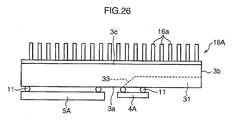
- a plurality of thermal via 16B may be provided in the mount substrate 3, so that the heat generated by the light emitting element 4A and the IC substrate 5A is dissipated by the thermal via 16B.
- the thermal via 16B is formed by filling a metal, such as copper, having high thermal conductivity in a through hole.
- a heat dissipating component 16C constituted by a material, such as copper, having a relatively high thermal conductivity may also be provided between the interposer substrate 8 and both of the light emitting elements 4A and the IC substrates 5A which are mounted on the one surface 3a of the mount substrate 3, so that the heat dissipating component 16C is in contact with the interposer substrate 8 and both of the light emitting element 4A and the IC substrate 5A.
- the heat generated by the light emitting element 4A and the IC substrate 5A is conducted to the interposer substrate 8 via the heat dissipating component 16C so as to be dissipated.
- the heat generated by the light emitting element 4A and the IC substrate 5A is conducted to the interposer substrate 8 via the heat dissipating component 16C so as to be dissipated.
- the heat dissipating component 16C needs only be in contact with the interposer substrate 8 and at least one of the light emitting element 4A and the IC substrate 5A, and hence, for example, the heat dissipating component 16C may be adapted to be in contact only with the interposer substrate 8 and the light emitting element 4A.
- a half mirror portion 31c inclined in the direction substantially perpendicular to the mirror portion 33 is provided in the middle of the internal waveguide 31, and a light receiving element 17 for monitoring is mounted at a position corresponding to the half mirror portion 31c, on the one surface 3a of the mount substrate 3.
- the provision of the half mirror portion 31c in the middle of the internal waveguide 31 may be effected by forming a slit in the internal waveguide 31 and inserting the half mirror in the slit.
- the half mirror potion 31c reflects several percent of the light which is emitted by the light emitting element 4A and reflected by the mirror portion 33, and transmits the rest of the light. For this reason, a part of the light emitted by the light emitting element 4A is received by the light receiving element 17 for monitoring.
- the light receiving element 17 for monitoring outputs the output of the light emitting element 4A as a monitor signal by receiving the light in this way.
- a protrusion (not shown) is provided in the groove 32 for waveguide formation, and the leading edge of the protrusion is constituted as a mirror so as to intrude into the core 31a, thereby making a part of the light waveguided by the core 31a reflected to the light receiving element 17 for monitoring by the leading edge of the protrusion.
- the monitor signal output from the light receiving element 17 for monitoring is sent to the IC substrate 5A via a wiring pattern 36b formed on the one surface 3a of the mount substrate 3.
- the IC circuit 50A formed in the IC substrate 5A includes a control circuit (not shown) which adjusts the electric signal transmitted to the light emitting element 4A via a wiring pattern 36a. On the basis of the monitor signal output from the light receiving element 17 for monitoring, the control circuit adjusts the electric signal so as to make the output of the light emitting element 4A constant.
- the branch 313 may be formed in the core 31a of the internal waveguide 31 to form a branch path 31a', so that the light receiving element 17 for monitoring is provided at a position corresponding to the leading edge of the branch path 31a'.
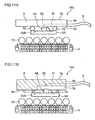
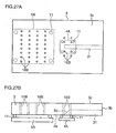
- a recess 18 in which the solder ball 11' can be fit is provided at a position corresponding to the solder ball 11', on the one surface 3a of the mount substrate 3.
- the recess 18 is constituted by a groove formed on the one surface 3a of the mount substrate 3.
- the solder ball 11' can be positioned with high precision by the recess 18 provided on the one surface 3a of the mount substrate 3, which makes it possible to improve the positioning accuracy of the light emitting element 4A, and to reduce the optical coupling loss between the light emitting element 4A and the internal waveguide 31 caused by the mounting position deviation of the light emitting element 4A.
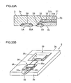
- the recess 18 can also be constituted by a solder paste 18A as shown in Fig. 32A and Fig. 32B . That is, the solder paste 18A having the recess 18 can be simply formed by applying the solder in the shape of a circle at the time of application.
- the interposer substrate 8 is provided as in the third embodiment and the fifth embodiment, it is possible to reduce the size of the solder ball 15 in correspondence with the amount by which the light emitting element 4A and the IC substrate 5A are dropped, while in the case where the interposer substrate 8 is not provided as in the first embodiment and the second embodiment, it is possible to reduce the size of the solder ball 10 in correspondence with the amount by which the light emitting element 4A and the IC substrate 5A are dropped.
- the end 141 of the electric circuit film 14 is joined to the upper surface of the interposer substrate 8 as shown in Fig. 34A , so that the conductive line 14a is directly connected to the interposer substrate 8.
- the conductive line 14a is also possible to directly connect the conductive line 14a to the mount substrate 3.
- the conductive line 14a is adapted to be directly connected to the interposer substrate 8 as shown in Fig. 34A
- the wiring pattern 36 to be formed on the mount substrate 3 can be reduced more than the case where the conductive line 14a is directly connected to the mount substrate 3. This makes it possible to reduce the size of the mount substrate 3, and also to prevent the effect of the noise source such as the power source line constituted by the conductive line 14a from being transmitted to the mount substrate. Further, this makes it possible to form a number of electric signal lines.
- Fig. 34B it is possible to connect the conductive line 14a to both the upper and lower surfaces of the interposer substrate 8 in such a manner that the end 141 of the electric circuit film 14 is divided into two, and one end 141 is joined to the upper surface of the interposer substrate 8, and the other end 141 is joined to the lower surface of the interposer substrate 8.
- the present invention provides a photoelectric converter characterized by including: a mount substrate; an IC circuit provided on the mount substrate; an optical element adapted to have a function of converting an electric signal output from the IC circuit into an optical signal and emitting light or a function of converting a received optical signal to an electric signal and outputting the electric signal to the IC circuit; and a waveguide adapted to effect an optical coupling between the optical element and an external optical device, and in that the optical element is held by the mount substrate and has a light emitting surface or a light receiving surface, the light emitting surface or the light receiving surface of the optical element being directed toward the surface of the mount substrate, and in that the waveguide is provided in the mount substrate along the surface of the mount substrate.
- the waveguide is provided along the surface of a mount substrate, which makes it possible to suppress the height of the whole device in the thickness direction of the mount substrate, and to achieve the low height of the device.
- the photoelectric converter further includes an electric connector which is provided on either one surface or the other surface of the mount substrate, and is capable of electrically connecting the IC circuit to an external connector.
- the one surface and the other surface of the mount substrate mean both surfaces in the thickness direction of the mount substrate.
- the electric connector is provided on the one surface of the mount substrate on which the optical element is mounted, or on the other surface opposite the one surface, to thereby make it possible to electrically connect the IC circuit to the external connector.
- the waveguide preferably includes: a mirror portion adapted to convert the optical path of the optical signal by approximately 90 degrees; an internal waveguide adapted to be provided so as to extend from the mirror portion to the end surface of the mount substrate; and an external waveguide adapted to optically couple the internal waveguide to the external optical device, which is joined to the end surface of the mount substrate.
- the waveguide by providing a through hole at a position corresponding to the optical element of the mount substrate, and providing an optical fiber, or the like, whose end is cut at an angle of 45 degrees, on the other surface of the mount substrate.
- the waveguide is constituted by the mirror portion and the internal waveguide which are provided in the mount substrate and by the external waveguide joined to the end surface of the mount substrate, it is possible to reduce the height of the device more as compared with the constitution as described above.
- the mount substrate is preferably a silicon substrate.
- the mount substrate is a silicon substrate in this way, the mirror portion and the internal waveguide can be easily formed.
- an electric connector is provided with a recessed portion in which the mount substrate can be fit, and the bottom surface of the recessed portion is joined to the one surface or other surface of the mount substrate.
- the recessed portion in which the mount substrate can be fit is provided in the electric connector, which makes it possible to further reduce the height of the device.
- a wiring substrate for changing the electrode pattern is interposed between the mount substrate and the electric connector.
- the wiring substrate is a freely bendable flexible substrate extending in the direction in which the waveguide extends, and that an electric circuit for transmitting/receiving power to/from the other photoelectric converter is formed in the wiring substrate.
- the wiring substrate is a flexible substrate, which makes it possible to bend the wiring substrate together with the waveguide.
- a conductive line for transmitting/receiving power to/from the other photoelectric converter is provided for the waveguide, and the conductive line is directly connected to the electric connector.
- the conductive line for the waveguide By providing the conductive line for the waveguide in this way, electric wiring with the other photoelectric converter can be performed by utilizing the waveguide. Further, the conductive line is directly connected to the electric connector, which makes it possible to effect the electric connection for an electric signal and the electric connection for transmission or reception of power by the single electric connector.
- a plurality of light emitting elements which emit light beams of wavelengths different from each other, are mounted on the mount substrate as the optical element, and the waveguide has a plurality of incident portions optically coupled to the respective light emitting elements, and one emitting portion connected to the incident portions.
- the plurality of light beams having different wavelengths are adapted to be propagated by the waveguide in a superimposed state, so that it is possible to significantly increase the amount of data which can be sent by a single device.
- a light emitting element is mounted as the optical element on the mount substrate, and the waveguide includes an incident portion optically coupled to the light emitting element and a plurality of emitting portions connected to the incident portion.
- the light beam emitted by the light emitting element is adapted to be distributed and propagated by the waveguide, which enables one-to-many data transmission.
- heat dissipating means for dissipating heat generated by the optical element is provided on the mount substrate.
- the heat generated by the optical element is dissipated by the heat dissipating means, which makes it possible to suppress the effect of the heat generated by the optical element.
- an IC substrate which has the IC circuit formed therein and is mounted on the mount substrate is further provided, the wiring substrate is interposed between the mount substrate and the electric connector, and a heat dissipating component having a relatively high thermal conductivity is arranged between the wiring substrate and the mount substrate, so as to be in contact both with the wiring substrate and with at least one of the optical element and the IC substrate which are mounted on the mount substrate.
- the heat generated by the optical element or the IC substrate is adapted to be conducted to the wiring substrate via the heat dissipating component and dissipated, which makes it possible to dissipate the heat generated by the optical element or the IC substrate by rationally utilizing the wiring substrate.
- a light emitting element as the optical element and a light receiving element for monitoring which outputs an output of the light emitting element as a monitor signal by receiving a part of the light emitted by the light emitting element are mounted on the mount substrate, and that the IC circuit includes a control circuit adapted to adjust an electric signal transmitted to the light emitting element so as to make the output of the light emitting element constant, on the basis of the monitor signal output from the light receiving element for monitoring.
- the output of the light emitting element can be made constant without being influenced by the environment, such as temperature.
- the optical element is mounted on the mount substrate by means of solder balls, and a recess in which the solder ball can be fit is provided on the mount substrate at a position where the solder ball is arranged.
- the solder ball can be positioned with high precision by the recess provided on the one surface of the mount substrate, which makes it possible to improve the positioning accuracy of the optical element and to reduce the optical coupling loss between the optical element and the waveguide caused by the mounting position deviation of the optical element.
- a recessed portion in which the optical element is dropped is provided in the mount substrate.
- a conductive line for transmitting/receiving power to/from the other photoelectric converter is provided and directly connected to the wiring substrate.
- the conductive line for transmitting/receiving power to/from the other photoelectric converter is provided in the waveguide, it is also possible to directly connect the conductive line to the mount substrate.
- the conductive line is adapted to be directly connected to the wiring substrate, it is possible to reduce the wiring pattern to be formed on the mount substrate more than the case where the conductive line is directly connected to the mount substrate.
Landscapes
- Physics & Mathematics (AREA)
- General Physics & Mathematics (AREA)
- Optics & Photonics (AREA)
- Optical Couplings Of Light Guides (AREA)
- Optical Integrated Circuits (AREA)
- Light Receiving Elements (AREA)
Applications Claiming Priority (4)
| Application Number | Priority Date | Filing Date | Title |
|---|---|---|---|
| JP2006218776 | 2006-08-10 | ||
| JP2006268999A JP4882644B2 (ja) | 2006-08-10 | 2006-09-29 | 光電気変換装置 |
| PCT/JP2007/065887 WO2008018620A1 (en) | 2006-08-10 | 2007-08-08 | Photoelectric converter |
| EP07792527.9A EP2059841B1 (de) | 2006-08-10 | 2007-08-08 | Fotoelektrischer wandler |
Related Parent Applications (3)
| Application Number | Title | Priority Date | Filing Date |
|---|---|---|---|
| EP07792527.9A Division-Into EP2059841B1 (de) | 2006-08-10 | 2007-08-08 | Fotoelektrischer wandler |
| EP07792527.9A Division EP2059841B1 (de) | 2006-08-10 | 2007-08-08 | Fotoelektrischer wandler |
| EP07792527.9 Division | 2007-08-08 |
Publications (3)
| Publication Number | Publication Date |
|---|---|
| EP2365363A2 true EP2365363A2 (de) | 2011-09-14 |
| EP2365363A3 EP2365363A3 (de) | 2011-09-21 |
| EP2365363B1 EP2365363B1 (de) | 2020-11-11 |
Family
ID=38727475
Family Applications (2)
| Application Number | Title | Priority Date | Filing Date |
|---|---|---|---|
| EP07792527.9A Active EP2059841B1 (de) | 2006-08-10 | 2007-08-08 | Fotoelektrischer wandler |
| EP11004806.3A Active EP2365363B1 (de) | 2006-08-10 | 2007-08-08 | Fotoelektrischer Wandler |
Family Applications Before (1)
| Application Number | Title | Priority Date | Filing Date |
|---|---|---|---|
| EP07792527.9A Active EP2059841B1 (de) | 2006-08-10 | 2007-08-08 | Fotoelektrischer wandler |
Country Status (6)
| Country | Link |
|---|---|
| US (1) | US8575529B2 (de) |
| EP (2) | EP2059841B1 (de) |
| JP (1) | JP4882644B2 (de) |
| KR (1) | KR101139554B1 (de) |
| TW (1) | TWI360674B (de) |
| WO (1) | WO2008018620A1 (de) |
Families Citing this family (45)
| Publication number | Priority date | Publication date | Assignee | Title |
|---|---|---|---|---|
| JP2009258341A (ja) * | 2008-04-16 | 2009-11-05 | Japan Aviation Electronics Industry Ltd | 光モジュール、光電変換器 |
| JP4661931B2 (ja) * | 2008-09-24 | 2011-03-30 | オムロン株式会社 | 光伝送モジュール、光伝送モジュールの製造方法、及び電子機器 |
| US9011177B2 (en) | 2009-01-30 | 2015-04-21 | Molex Incorporated | High speed bypass cable assembly |
| JP5168175B2 (ja) * | 2009-02-04 | 2013-03-21 | 日立電線株式会社 | 光伝送モジュール |
| JP5515377B2 (ja) * | 2009-04-03 | 2014-06-11 | 住友電気工業株式会社 | 複合ハーネス及びその製造方法 |
| JP5185895B2 (ja) * | 2009-07-29 | 2013-04-17 | パナソニック株式会社 | 光電変換サブマウント基板及びその製造方法 |
| JP2011095333A (ja) * | 2009-10-27 | 2011-05-12 | Toshiba Corp | 実装構造体 |
| TW201211606A (en) | 2010-09-03 | 2012-03-16 | Univ Nat Central | Optical transmission module with optical waveguide structure |
| JP5654316B2 (ja) * | 2010-10-29 | 2015-01-14 | パナソニックIpマネジメント株式会社 | 光モジュール |
| US9057850B2 (en) * | 2011-03-24 | 2015-06-16 | Centera Photonics Inc. | Optoelectronic module |
| JP5954934B2 (ja) * | 2011-04-04 | 2016-07-20 | 富士通コンポーネント株式会社 | コネクタ |
| JP2014044409A (ja) * | 2012-07-30 | 2014-03-13 | Kyocera Corp | 光装置用部品、光装置および光モジュール |
| US9319148B2 (en) | 2012-10-01 | 2016-04-19 | Lenovo Enterprise Solutions (Singapore) Pte. Ltd. | Optical interconnection to an integrated circuit |
| US9142921B2 (en) | 2013-02-27 | 2015-09-22 | Molex Incorporated | High speed bypass cable for use with backplanes |
| JP2014186262A (ja) * | 2013-03-25 | 2014-10-02 | Nippon Telegr & Teleph Corp <Ntt> | 集積型光回路素子 |
| JP2015023143A (ja) * | 2013-07-18 | 2015-02-02 | 富士通コンポーネント株式会社 | 光モジュール |
| JP2015049256A (ja) * | 2013-08-29 | 2015-03-16 | 住友ベークライト株式会社 | 光モジュール用部材、光モジュールおよび電子機器 |
| WO2015035052A1 (en) | 2013-09-04 | 2015-03-12 | Molex Incorporated | Connector system with cable by-pass |
| JP6190247B2 (ja) * | 2013-11-08 | 2017-08-30 | 日本電信電話株式会社 | 配線基板 |
| US9325420B2 (en) * | 2014-05-16 | 2016-04-26 | Qualcomm Incorporated | Electro-optical transceiver device to enable chip-to-chip interconnection |
| US9377596B2 (en) * | 2014-07-22 | 2016-06-28 | Unimicron Technology Corp. | Optical-electro circuit board, optical component and manufacturing method thereof |
| CN110662388A (zh) | 2015-01-11 | 2020-01-07 | 莫列斯有限公司 | 模块壳体及连接器端口 |
| KR20170102011A (ko) * | 2015-01-11 | 2017-09-06 | 몰렉스 엘엘씨 | 바이패스 루트설정 조립체에 사용하기 적합한 와이어-대-기판 커넥터 |
| WO2016140855A1 (en) * | 2015-03-05 | 2016-09-09 | Corning Optical Communications LLC | A connector device for connecting at least one optical fiber end piece to an electric terminal |
| EP3271765A1 (de) * | 2015-03-19 | 2018-01-24 | Corning Optical Communications LLC | Verbindervorrichtung zum verbinden von wenigstens einem glasfaserendstück und herstellungsverfahren |
| WO2016179263A1 (en) | 2015-05-04 | 2016-11-10 | Molex, Llc | Computing device using bypass assembly |
| US10409015B1 (en) | 2015-12-15 | 2019-09-10 | Optomind Inc. | Optical receiving device including focusing lens and reflector mounted to housing body and collimating lens mounted to housing cover |
| WO2017105110A1 (ko) | 2015-12-15 | 2017-06-22 | (주)옵토마인드 | 광 케이블용 송수신 장치 및 그 정렬 방법 |
| US10424878B2 (en) | 2016-01-11 | 2019-09-24 | Molex, Llc | Cable connector assembly |
| KR102092627B1 (ko) | 2016-01-11 | 2020-03-24 | 몰렉스 엘엘씨 | 루트설정 조립체 및 이를 사용한 시스템 |
| CN108475870B (zh) | 2016-01-19 | 2019-10-18 | 莫列斯有限公司 | 集成路由组件以及采用集成路由组件的系统 |
| JP6664255B2 (ja) * | 2016-03-29 | 2020-03-13 | ホシデン株式会社 | 光ファイバアレイと光モジュールとの接続構造 |
| CN116661072A (zh) | 2017-09-24 | 2023-08-29 | 申泰公司 | 有通用定位的光收发器 |
| US10910748B2 (en) * | 2017-11-13 | 2021-02-02 | Te Connectivity Corporation | Cable socket connector assembly for an electronic |
| US10866373B2 (en) | 2018-06-27 | 2020-12-15 | Taiwan Semiconductor Manufacturing Company, Ltd. | Optical transceiver and manufacturing method thereof |
| US10903594B2 (en) * | 2018-10-01 | 2021-01-26 | Te Connectivity Corporation | Board-to-board connector assembly for add-in cards |
| EP3789805B1 (de) * | 2019-09-04 | 2023-08-09 | Ams Ag | Verbundstruktur und verfahren zur herstellung einer verbundstruktur |
| US11624882B2 (en) * | 2019-09-13 | 2023-04-11 | Avicenatech Corp. | Optical interconnects using microLEDs |
| JPWO2021162108A1 (de) * | 2020-02-12 | 2021-08-19 | ||
| CN116325370A (zh) * | 2020-10-13 | 2023-06-23 | 申泰公司 | 用于高速数据传输的具有环形连接器的竖直插入互连系统 |
| US20230387631A1 (en) * | 2020-10-13 | 2023-11-30 | Samtec, Inc. | Vertical interconnect system for high-speed data transmission |
| CN215266745U (zh) * | 2020-12-29 | 2021-12-21 | 番禺得意精密电子工业有限公司 | 连接器组件 |
| US12332490B2 (en) * | 2021-09-24 | 2025-06-17 | Hirose Electric Co., Ltd. | Media adaptor for multimode waveguide interconnects |
| US20230400648A1 (en) * | 2022-06-10 | 2023-12-14 | Advanced Semiconductor Engineering, Inc. | Electronic package |
| TWI905819B (zh) * | 2024-06-26 | 2025-11-21 | 大陸商鵬鼎控股(深圳)股份有限公司 | 電子裝置及其製造方法 |
Citations (1)
| Publication number | Priority date | Publication date | Assignee | Title |
|---|---|---|---|---|
| JP2001042170A (ja) | 1999-07-28 | 2001-02-16 | Canon Inc | 光配線装置、その駆動方法およびそれを用いた電子機器 |
Family Cites Families (32)
| Publication number | Priority date | Publication date | Assignee | Title |
|---|---|---|---|---|
| US4904036A (en) * | 1988-03-03 | 1990-02-27 | American Telephone And Telegraph Company, At&T Bell Laboratories | Subassemblies for optoelectronic hybrid integrated circuits |
| JP2762792B2 (ja) * | 1991-08-30 | 1998-06-04 | 日本電気株式会社 | 光半導体装置 |
| US5345524A (en) * | 1993-05-20 | 1994-09-06 | Motorola, Inc. | Optoelectronic transceiver sub-module and method for making |
| JP3658426B2 (ja) * | 1995-01-23 | 2005-06-08 | 株式会社日立製作所 | 光半導体装置 |
| US5835646A (en) * | 1995-09-19 | 1998-11-10 | Fujitsu Limited | Active optical circuit sheet or active optical circuit board, active optical connector and optical MCM, process for fabricating optical waveguide, and devices obtained thereby |
| JP3705873B2 (ja) * | 1996-10-17 | 2005-10-12 | 株式会社アドバンテスト | 光・電気混在配線板 |
| DE19732180A1 (de) | 1997-07-25 | 1999-02-18 | Siemens Ag | Digitaler Schaltkreis in MOS-Technologie |
| US5987196A (en) * | 1997-11-06 | 1999-11-16 | Micron Technology, Inc. | Semiconductor structure having an optical signal path in a substrate and method for forming the same |
| JP3715425B2 (ja) * | 1998-03-06 | 2005-11-09 | ブラザー工業株式会社 | 光導波路付基板の製造方法 |
| WO2000008505A1 (fr) * | 1998-08-05 | 2000-02-17 | Seiko Epson Corporation | Module optique |
| US6785447B2 (en) * | 1998-10-09 | 2004-08-31 | Fujitsu Limited | Single and multilayer waveguides and fabrication process |
| US6706546B2 (en) * | 1998-10-09 | 2004-03-16 | Fujitsu Limited | Optical reflective structures and method for making |
| US6684007B2 (en) * | 1998-10-09 | 2004-01-27 | Fujitsu Limited | Optical coupling structures and the fabrication processes |
| DE60027342T2 (de) * | 1999-03-26 | 2007-01-04 | Seiko Epson Corp. | Flexible gedruckte Leiterplatte, elektrooptische Vorrichtung, und elektronisches Gerät |
| JP2000292656A (ja) * | 1999-04-01 | 2000-10-20 | Sony Corp | 光伝送装置および光伝送装置の製造方法 |
| JP3630116B2 (ja) * | 2000-08-10 | 2005-03-16 | セイコーエプソン株式会社 | 電気光学ユニットおよび電子機器 |
| US7289701B2 (en) * | 2002-03-14 | 2007-10-30 | Sae Magnetics (Hong Kong) Limited | Integrated platform for passive optical alignment of semiconductor device with optical fiber |
| CN1215545C (zh) | 2002-03-29 | 2005-08-17 | 株式会社东芝 | 半导体测试装置 |
| US7110629B2 (en) * | 2002-07-22 | 2006-09-19 | Applied Materials, Inc. | Optical ready substrates |
| JP3960905B2 (ja) | 2002-11-11 | 2007-08-15 | アルプス電気株式会社 | 面実装型回路モジュール |
| JP2005077640A (ja) * | 2003-08-29 | 2005-03-24 | Ngk Spark Plug Co Ltd | 光導波路付き配線基板 |
| JP2005158008A (ja) | 2003-11-06 | 2005-06-16 | Matsushita Electric Ind Co Ltd | タッチパネルおよびこれを用いたタッチパネル付き液晶表示装置 |
| JPWO2005052666A1 (ja) * | 2003-11-27 | 2008-03-06 | イビデン株式会社 | Icチップ実装用基板、マザーボード用基板、光通信用デバイス、icチップ実装用基板の製造方法、および、マザーボード用基板の製造方法 |
| KR20070085080A (ko) * | 2004-02-18 | 2007-08-27 | 컬러 칩 (이스라엘) 리미티드. | 전자-광 모듈 제조 시스템 및 방법 |
| JP4138689B2 (ja) * | 2004-03-30 | 2008-08-27 | 株式会社東芝 | インターフェイスモジュール付lsiパッケージ及びlsiパッケージ |
| US7306378B2 (en) * | 2004-05-06 | 2007-12-11 | Intel Corporation | Method and apparatus providing an electrical-optical coupler |
| JP2006003818A (ja) * | 2004-06-21 | 2006-01-05 | Mitsubishi Electric Corp | 半導体集積回路チップ及びその製造方法 |
| CN1243286C (zh) | 2004-08-14 | 2006-02-22 | 浙江大学 | 基于硅衬底的聚合物光波导器件的制作方法 |
| KR100734906B1 (ko) * | 2005-06-21 | 2007-07-03 | 한국정보통신대학교 산학협력단 | 연성 광 pcb를 이용한 광연결 장치 |
| JP2007295197A (ja) * | 2006-04-24 | 2007-11-08 | Matsushita Electric Ind Co Ltd | Δς変調器及びa/d変換器 |
| JP4829695B2 (ja) * | 2006-06-16 | 2011-12-07 | パナソニック株式会社 | A/d変換器 |
| JP2008278062A (ja) * | 2007-04-26 | 2008-11-13 | Matsushita Electric Ind Co Ltd | 固体撮像装置、ad変換器、ad変換方法 |
-
2006
- 2006-09-29 JP JP2006268999A patent/JP4882644B2/ja active Active
-
2007
- 2007-08-08 WO PCT/JP2007/065887 patent/WO2008018620A1/en not_active Ceased
- 2007-08-08 US US12/376,891 patent/US8575529B2/en active Active
- 2007-08-08 KR KR1020097004643A patent/KR101139554B1/ko not_active Expired - Fee Related
- 2007-08-08 EP EP07792527.9A patent/EP2059841B1/de active Active
- 2007-08-08 EP EP11004806.3A patent/EP2365363B1/de active Active
- 2007-08-09 TW TW096129354A patent/TWI360674B/zh active
Patent Citations (1)
| Publication number | Priority date | Publication date | Assignee | Title |
|---|---|---|---|---|
| JP2001042170A (ja) | 1999-07-28 | 2001-02-16 | Canon Inc | 光配線装置、その駆動方法およびそれを用いた電子機器 |
Also Published As
| Publication number | Publication date |
|---|---|
| EP2059841B1 (de) | 2015-07-08 |
| JP2008065287A (ja) | 2008-03-21 |
| KR20090040365A (ko) | 2009-04-23 |
| US8575529B2 (en) | 2013-11-05 |
| EP2059841A1 (de) | 2009-05-20 |
| KR101139554B1 (ko) | 2012-04-27 |
| TWI360674B (en) | 2012-03-21 |
| EP2365363A3 (de) | 2011-09-21 |
| TW200809291A (en) | 2008-02-16 |
| US20100171023A1 (en) | 2010-07-08 |
| EP2365363B1 (de) | 2020-11-11 |
| WO2008018620A1 (en) | 2008-02-14 |
| JP4882644B2 (ja) | 2012-02-22 |
Similar Documents
| Publication | Publication Date | Title |
|---|---|---|
| EP2059841B1 (de) | Fotoelektrischer wandler | |
| JP5457656B2 (ja) | 光電気変換装置 | |
| US6635866B2 (en) | Multi-functional fiber optic coupler | |
| CN106371176B (zh) | 具有改善的热管理的光电模块 | |
| JP4830607B2 (ja) | 光電気変換装置及びその製造方法並びに外部導波路 | |
| US20120257852A1 (en) | Optical module, manufacturing method of optical module and optical communication device | |
| CN216351374U (zh) | 一种光模块 | |
| US20250219350A1 (en) | Optical system-in-package, and optical module and optical transceiver using same | |
| WO2007091733A2 (en) | Photoelectric converting device, manufacturing method of the same, and external waveguide | |
| CN101523264A (zh) | 光电变换装置 | |
| KR20080028488A (ko) | 광 케이블 및 송수신 서브 어셈블리 | |
| JP4876830B2 (ja) | 光電気変換装置 | |
| KR100937246B1 (ko) | 광학벤치를 이용한 수동정렬형 광부모듈 및 그 제조방법 | |
| JP4739987B2 (ja) | 光ファイバ接続構造及び光ファイバ接続方法 | |
| JP2002296464A (ja) | 光電気配線基板 | |
| US20250264666A1 (en) | Optical module | |
| JP4779919B2 (ja) | 光電気変換装置 | |
| JP4779918B2 (ja) | 光電気変換装置 | |
| JP2011059360A (ja) | 光モジュール及光モジュールの製造方法 | |
| JP2008091516A (ja) | 光電気変換装置 | |
| JP4779920B2 (ja) | 光電気変換装置 | |
| JP2005222003A (ja) | マウント、光部品、光送受信モジュール及び双方向光通信モジュール | |
| JP2008091515A (ja) | 光電気変換装置 | |
| JP2005077858A (ja) | 光モジュール、光伝送装置及び光伝送システム | |
| JP2008091493A (ja) | 光電気変換装置 |
Legal Events
| Date | Code | Title | Description |
|---|---|---|---|
| PUAI | Public reference made under article 153(3) epc to a published international application that has entered the european phase |
Free format text: ORIGINAL CODE: 0009012 |
|
| PUAL | Search report despatched |
Free format text: ORIGINAL CODE: 0009013 |
|
| AC | Divisional application: reference to earlier application |
Ref document number: 2059841 Country of ref document: EP Kind code of ref document: P |
|
| AK | Designated contracting states |
Kind code of ref document: A2 Designated state(s): DE FR GB IT |
|
| AK | Designated contracting states |
Kind code of ref document: A3 Designated state(s): DE FR GB IT |
|
| RIC1 | Information provided on ipc code assigned before grant |
Ipc: G02B 6/43 20060101ALI20110817BHEP Ipc: G02B 6/42 20060101AFI20110817BHEP |
|
| RAP1 | Party data changed (applicant data changed or rights of an application transferred) |
Owner name: PANASONIC CORPORATION |
|
| 17P | Request for examination filed |
Effective date: 20120320 |
|
| 17Q | First examination report despatched |
Effective date: 20140424 |
|
| RAP1 | Party data changed (applicant data changed or rights of an application transferred) |
Owner name: PANASONIC INTELLECTUAL PROPERTY MANAGEMENT CO., LT |
|
| RAP1 | Party data changed (applicant data changed or rights of an application transferred) |
Owner name: PANASONIC INTELLECTUAL PROPERTY MANAGEMENT CO., LT |
|
| STAA | Information on the status of an ep patent application or granted ep patent |
Free format text: STATUS: EXAMINATION IS IN PROGRESS |
|
| GRAP | Despatch of communication of intention to grant a patent |
Free format text: ORIGINAL CODE: EPIDOSNIGR1 |
|
| STAA | Information on the status of an ep patent application or granted ep patent |
Free format text: STATUS: GRANT OF PATENT IS INTENDED |
|
| INTG | Intention to grant announced |
Effective date: 20200619 |
|
| GRAS | Grant fee paid |
Free format text: ORIGINAL CODE: EPIDOSNIGR3 |
|
| GRAA | (expected) grant |
Free format text: ORIGINAL CODE: 0009210 |
|
| STAA | Information on the status of an ep patent application or granted ep patent |
Free format text: STATUS: THE PATENT HAS BEEN GRANTED |
|
| AC | Divisional application: reference to earlier application |
Ref document number: 2059841 Country of ref document: EP Kind code of ref document: P |
|
| AK | Designated contracting states |
Kind code of ref document: B1 Designated state(s): DE FR GB IT |
|
| REG | Reference to a national code |
Ref country code: GB Ref legal event code: FG4D |
|
| REG | Reference to a national code |
Ref country code: DE Ref legal event code: R096 Ref document number: 602007060773 Country of ref document: DE |
|
| REG | Reference to a national code |
Ref country code: DE Ref legal event code: R097 Ref document number: 602007060773 Country of ref document: DE |
|
| PLBE | No opposition filed within time limit |
Free format text: ORIGINAL CODE: 0009261 |
|
| STAA | Information on the status of an ep patent application or granted ep patent |
Free format text: STATUS: NO OPPOSITION FILED WITHIN TIME LIMIT |
|
| 26N | No opposition filed |
Effective date: 20210812 |
|
| PG25 | Lapsed in a contracting state [announced via postgrant information from national office to epo] |
Ref country code: IT Free format text: LAPSE BECAUSE OF FAILURE TO SUBMIT A TRANSLATION OF THE DESCRIPTION OR TO PAY THE FEE WITHIN THE PRESCRIBED TIME-LIMIT Effective date: 20201111 |
|
| GBPC | Gb: european patent ceased through non-payment of renewal fee |
Effective date: 20210808 |
|
| PG25 | Lapsed in a contracting state [announced via postgrant information from national office to epo] |
Ref country code: GB Free format text: LAPSE BECAUSE OF NON-PAYMENT OF DUE FEES Effective date: 20210808 Ref country code: FR Free format text: LAPSE BECAUSE OF NON-PAYMENT OF DUE FEES Effective date: 20210831 |
|
| PGFP | Annual fee paid to national office [announced via postgrant information from national office to epo] |
Ref country code: DE Payment date: 20250820 Year of fee payment: 19 |