EP2365523B1 - Stressresistente Microvia-Struktur für flexible Schaltungen - Google Patents
Stressresistente Microvia-Struktur für flexible Schaltungen Download PDFInfo
- Publication number
- EP2365523B1 EP2365523B1 EP11156492.8A EP11156492A EP2365523B1 EP 2365523 B1 EP2365523 B1 EP 2365523B1 EP 11156492 A EP11156492 A EP 11156492A EP 2365523 B1 EP2365523 B1 EP 2365523B1
- Authority
- EP
- European Patent Office
- Prior art keywords
- thickness
- metal
- layer
- polyimide flex
- sidewall
- Prior art date
- Legal status (The legal status is an assumption and is not a legal conclusion. Google has not performed a legal analysis and makes no representation as to the accuracy of the status listed.)
- Active
Links
Images


Classifications
-
- H—ELECTRICITY
- H10—SEMICONDUCTOR DEVICES; ELECTRIC SOLID-STATE DEVICES NOT OTHERWISE PROVIDED FOR
- H10W—GENERIC PACKAGES, INTERCONNECTIONS, CONNECTORS OR OTHER CONSTRUCTIONAL DETAILS OF DEVICES COVERED BY CLASS H10
- H10W70/00—Package substrates; Interposers; Redistribution layers [RDL]
- H10W70/60—Insulating or insulated package substrates; Interposers; Redistribution layers
- H10W70/67—Insulating or insulated package substrates; Interposers; Redistribution layers characterised by their insulating layers or insulating parts
- H10W70/688—Flexible insulating substrates
-
- H—ELECTRICITY
- H10—SEMICONDUCTOR DEVICES; ELECTRIC SOLID-STATE DEVICES NOT OTHERWISE PROVIDED FOR
- H10W—GENERIC PACKAGES, INTERCONNECTIONS, CONNECTORS OR OTHER CONSTRUCTIONAL DETAILS OF DEVICES COVERED BY CLASS H10
- H10W20/00—Interconnections in chips, wafers or substrates
- H10W20/20—Interconnections within wafers or substrates, e.g. through-silicon vias [TSV]
-
- H—ELECTRICITY
- H10—SEMICONDUCTOR DEVICES; ELECTRIC SOLID-STATE DEVICES NOT OTHERWISE PROVIDED FOR
- H10W—GENERIC PACKAGES, INTERCONNECTIONS, CONNECTORS OR OTHER CONSTRUCTIONAL DETAILS OF DEVICES COVERED BY CLASS H10
- H10W70/00—Package substrates; Interposers; Redistribution layers [RDL]
- H10W70/60—Insulating or insulated package substrates; Interposers; Redistribution layers
- H10W70/62—Insulating or insulated package substrates; Interposers; Redistribution layers characterised by their interconnections
- H10W70/63—Vias, e.g. via plugs
- H10W70/635—Through-vias
-
- H—ELECTRICITY
- H10—SEMICONDUCTOR DEVICES; ELECTRIC SOLID-STATE DEVICES NOT OTHERWISE PROVIDED FOR
- H10W—GENERIC PACKAGES, INTERCONNECTIONS, CONNECTORS OR OTHER CONSTRUCTIONAL DETAILS OF DEVICES COVERED BY CLASS H10
- H10W70/00—Package substrates; Interposers; Redistribution layers [RDL]
- H10W70/60—Insulating or insulated package substrates; Interposers; Redistribution layers
- H10W70/67—Insulating or insulated package substrates; Interposers; Redistribution layers characterised by their insulating layers or insulating parts
- H10W70/68—Shapes or dispositions thereof
- H10W70/685—Shapes or dispositions thereof comprising multiple insulating layers
Definitions
- Embodiments of the invention relate generally to chip packages and, more particularly, to chip packages having vias formed through dielectric and adhesive layers down to die pads of an electronic chip, with the vias having stress-resistant metal interconnects formed therein having an increased thickness.
- IC chip packaging technology is driven by ever-increasing needs for achieving better performance, greater miniaturization and higher reliability.
- semiconductor devices such as bare chips, have electrical contact pads or "die pads" located on a top-side or active surface of the device to provide input/output (I/O) connections.
- IC chips first packaging technologies such as the embedded chip build-up process (ECBU), generally apply a first dielectric layer (e.g., polyimide film) over a chip top surface, form vias in the dielectric layer such that they abut the die pads on the chip, and then form metal interconnections to the die pads along the vias and metal cover pads about the via openings on a top surface of the dielectric layer.
- ECBU embedded chip build-up process
- the metalized cover pad generally extends beyond the opening of the via. This additional level of interconnection redistributes the peripheral bonding pads of each chip to an area array of metal pads that are evenly deployed over the chip's surface. The solder balls or bumps used in connecting the device to the application circuit board are subsequently placed over these metal pads.
- the number of die pads on the chip is increased and the pad pitch (i.e., the center-to-center distance between adjacent die pads) is reduced, such as to 50 micrometers or less. This reduces the space available for via interconnect to the device, forcing smaller vias to be used (i.e., vias having a smaller diameter).
- the thickness of dielectric layers applied to the chip cannot be reduced, either because of impedance requirements between high frequency layers or due to dimension rigidity needed for pattern overlay alignment.
- the height/thickness of the vias extending through the dielectric layer remains somewhat constant, thereby resulting in vias having an increased aspect ratio (i.e., height-to-diameter ratio).
- Smaller diameter vias are harder to fill with metal during electroplating, and the total volume of metal present within such vias may be less for a given thickness compared to larger vias. That is, while the metal cover pads about the via openings on the top surface of the dielectric layer may be of a given thickness, the thickness of metal present within a smaller diameter via may be less than the given thickness based on the smaller diameter and an increased aspect ratio, thus reducing the volume of metal in the via below what is desired.
- This reduced volume of metal present in a reduced diameter via can lead to durability issues with the metal interconnect. That is, during thermal cycling reliability testing, stress from coefficient of thermal expansion (CTE) mismatch between the metal in the vias and the surrounding dielectric material eventually causes metal fatigue and cracking, resulting in loss/failure of the metal interconnect. This happens more quickly if there is less total metal present to minimize fatigue.
- CTE coefficient of thermal expansion
- the present invention provides for a chip package.
- the chip package includes vias formed through a dielectric layer down to die pads of an electronic chip, with the vias having stress-resistant metal interconnects formed therein having an increased thickness.
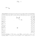
- bare electronic chip 10 includes a substrate 12 (e.g., silicon wafer) and a plurality of die pads 14 thereon.
- Die pads 14 may be placed on substrate 12 by a variety of techniques. For example, a metallization process or the like may be implemented to deposit die pads 14 onto substrate 12. Alternative techniques such as etching or photolithography may also be implemented.
- Die pads 14 may have a composition that includes a variety of materials such as, for example, aluminum, copper, gold, silver, and nickel, or combinations thereof. As shown in FIG. 1 , die pads 14 are arranged on substrate 12 such that they are spaced relative to one another. As such, each consecutive die pad 14 has a pitch 16 therebetween.
- Embodiments of the invention may use bare electronic chips having their die pads arranged in a manner different than that shown in FIG. 1 .
- other bare electronic chips may have multiple perimeter rows of die pads, rather than the single rows of die pads 14 shown in FIG. 1 .
- semiconductor devices may be used that have arrays of die pads located on any region of a substrate or one or more rows of die pads generally arranged over the center region of the substrate.
- Further embodiments may have die pads arranged along less than all four side of the perimeter of a substrate.
- embodiments of electronic chips may include die pads arranged such that the spacing between die pads varies.
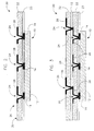
- a side view of a chip package 20 (i.e., integrated circuit (IC) package) is shown incorporating bare electronic chip 10.
- a free-standing dielectric layer such as a polyimide flex layer or circuit board 22
- an adhesive layer 23 applied therebetween, with the bare electronic chip 10 being attached to the adhesive layer 23 in a face-down orientation using a die attach mechanism (not shown) or some similar procedure.
- the polyimide flex layer 22 is in the form of a pre-formed laminate sheet or film that can be placed on bare electronic chip 10.
- the polyimide flex layer 22 can be formed of Kapton®, Ultem®, polytetrafluoroethylene (PTFE), or another polymer film, such as a liquid crystal polymer (LCP).
- adhesive layer 23 is comprised of an epoxy-based dielectric material, an epoxy resin, a photoacid generator, an antioxidant, and a cold catalyst corresponding to the photoacid generator, so as to provide an adhesive that promotes product reliability and yield.
- Adhesive layer is formed to have a thickness that provides for adequate bonding between polyimide flex layer 22 and electronic chip 10, such as a thickness in the range of 12 to 25 micrometers, for example.
- a plurality of vias 24 are formed in the laminate layer.
- the vias 24 are formed by way of a laser ablation or laser drilling process and are formed at positions corresponding to die pads 14 located on substrate 12. Laser drilling of vias 24 in polyimide flex layer 22 thus serves to expose the die pads 14.
- a metal layer/material 26 is applied onto polyimide flex layer 22 by way of, for example, a sputtering process, electroplating process, or combination of the two.
- the deposited metal layer/material 26 is then formed into metal interconnects 28.
- metal layer/material 26 is patterned and etched such that metal interconnects 28 are formed that extend from a top surface 30 of polyimide flex layer 22 and down through vias 24.
- Metal interconnects 28 thus form an electrical connection with die pads 14.
- polyimide flex layer 22 forms a re-distribution layer that acts to redistribute the arrangement of die pads 14, which may (as shown in FIG. 1 ) be arranged about a periphery of each bare electronic chip 10, into an area array of interconnects distributed over the surface of electronic chip package 20.
- one or more additional polyimide flex layers 32 are applied on polyimide flex layer 22 by way of associated adhesive layers 23 during construction of chip package 20, according to an embodiment of the invention. Similar to the steps set forth above, a plurality of vias 24 are formed in the additional polyimide flex layers 32 by way of, for example, a laser ablation or laser drilling process. The vias 24 in each of the additional polyimide flex layers 32 are formed at positions corresponding to metal interconnects 28 attached to a polyimide flex layer (e.g., polyimide flex layer 22) positioned immediately therebelow so as to allow for the further re-distribution of the metal interconnects 28.
- a polyimide flex layer e.g., polyimide flex layer 22
- metal interconnects are then again formed on the additional polyimide flex layer 32 via a deposition (e.g., sputtering or electroplating) process and subsequent patterning and etching process, so as to deform metal interconnects 28 to extend down through vias 24 and into electrical contact with metal interconnects 28 on a polyimide flex layer 22, 32 positioned immediately therebelow.
- a deposition e.g., sputtering or electroplating
- a thickness of metal interconnect 28 is dependent on a thickness of the adhesive layer 23 applied between substrate 12 and polyimide flex layer 22. That is, it is recognized that there is a high coefficient of thermal expansion (CTE) mismatch between the metal interconnect 28 formed in via 24 and the adhesive material forming layer 23. This high CTE mismatch can induce stress on metal interconnect 28, eventually causing metal fatigue and cracking and resulting in loss/failure of the metal interconnect. Thus, it is desired to provide a metal interconnect 28 having an increased thickness that fills a larger percentage volume of via 24 (or completely fills the vias) to provide improved resistance to metal fatigue and cracking, as compared to a thinner metal interconnect.
- CTE coefficient of thermal expansion
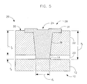
- a chip package 20 is provided according to an embodiment of the invention that includes a polyimide flex layer 22 formed to have a thickness t p of 25 micrometers, such that it is constructed as a free-standing film to which electronic chip 10 can be affixed.
- Adhesive layer 23 positioned between electronic chip 10 and polyimide flex layer 22 has a thickness t a of approximately 14 micrometers, so as to provide adequate bonding between polyimide flex layer 22 and electronic chip 10. Accordingly, via 24 formed through polyimide flex layer 22 and adhesive layer 23 has a height h 1 of approximately 39 micrometers.
- a metal interconnect 28 is formed on polyimide flex layer 22 and in via 24 by application of a metal layer/material, such as by an electroplating process and subsequent patterning and etching.
- Metal interconnect 28 is formed to include a cover pad 31 formed on top surface 30 of polyimide flex layer 22, a base section 34 that forms an electrical connection with die pad 14, and a sidewall 36 extending up from the base 34 along a perimeter of the via 24 and onto top surface 30 of polyimide flex layer 22. According to the embodiment of FIG.
- base 34 and sidewall 36 of metal interconnect 28 are formed to have a thickness t 1 in the range of 14 micrometers, so as to provide a metal interconnect 28 resistant to metal fatigue and cracking that may occur based on stresses imparted to the metal interconnect from a CTE mismatch between the metal forming metal interconnect 28 and the surrounding materials forming polyimide flex layer 22 and adhesive 23. That is, for a via 24 formed having a height h 1 of approximately 39 micrometers, where a thickness t a of adhesive layer 23 is 14 micrometers, a metal interconnect 28 having a base 34 and sidewall 36 thickness t 1 of 14 micrometers provides a metal interconnect having improved reliability with increased resistance to failure resulting from thermal cycling.
- an adhesive layer 23 may be provided between substrate 12 and polyidmide flex layer 22 having a thickness t a greater or lesser than 14 micrometers.
- a thickness t 1 of base 34 and sidewall 36 of metal interconnect 28 should be equal to or greater than a thickness t a of adhesive layer 23.
- a metal interconnect 28 having a base 34 and sidewall 36 with a thickness t 1 of at least 16 micrometers would be provided, according to an embodiment of the invention.
- Providing a metal interconnect 28 having a base 34 and sidewall 36 with a thickness t 1 equal to or greater than a thickness t a of adhesive layer 23, provides a reliable, stress-resistant metal interconnect 28.
- a chip package 20 is provided according to another embodiment of the invention that includes a polyimide flex layer 22 having a thickness t p of 25 micrometers, such that it is constructed as a free-standing film to which electronic chip 10 can be affixed.
- An adhesive layer 23 positioned between electronic chip 10 and polyimide flex layer 22 has a thickness t a of approximately 14 micrometers, so as to provide adequate bonding between polyimide flex layer 22 and electronic chip 10. Accordingly, via 24 formed through polyimide flex layer 22 and adhesive layer 23 has a height h 1 of approximately 39 micrometers.
- a metal interconnect 28 is provided having a cover pad 31 formed on top surface 30 of polyimide flex layer 22, along with a "base section" and “sidewall” in the form of a post interconnect 38 that fills (or substantially fills) via 24.
- a variety of "solid via plating" metallization techniques may be implemented to create post interconnect 38, such as by forming a solid metal in via 24 by implementing a selective pattern plate-up of the via metal or, through mechanisms of differential etching and plating rates, implement a pulsed plating that alternately plates and etches metal.
- post interconnect 38 can be described as a metal interconnect 28 having a "base section” and “sidewall” having a great enough thickness that via 24 is substantially or completely filled, thereby forming a post interconnect.
- post interconnect 38 fills via 24 it has a "thickness" greater than the thickness t a of adhesive layer 23, and thus provides a metal interconnect having improved reliability with increased resistance to failure resulting from thermal cycling.
- a diameter d 1 and aspect ratio (ratio of height to diameter) of via 24 may affect formation of the metal interconnect 28 during an electroplating process.
- a diameter d 1 of each via 24 is also decreased in order to allow for formation of vias corresponding to die pads 14 and the minimized pitch therebetween.
- a thickness t p of polyimide flex layer 22 e.g., a minimum polyimide flex layer thickness of 25 micrometers
- a reduction in the diameter d 1 , of each via 24 results in a via having an increased aspect ratio (i.e., ratio of height to diameter).
- the decreased diameter d 1 , and increased height-to-diameter aspect ratio of via 24 makes it harder to fill via 24 with metal during electroplating, thereby causing inconsistencies in the thickness of portions of metal interconnect 28. More specifically, the decreased diameter d 1 and increased height-to-diameter aspect ratio of via 24 can lead to a thickness t c of cover pad 31 being greater than a thickness t 1 of base 34 and sidewall 36. For example, such as shown in FIG.
- a thickness t c of cover pad 31 may be 8 micrometers while a thickness t 1 of base 34 and sidewall 36 may be approximately 5.5 micrometers, based on the inherent difficulty of filling via 24 with metal during electroplating.
- FIGS. 6A and 6B the relationship between metal interconnect reliability and a thickness t 1 of base 34 and sidewall 36 is illustrated, with a via string failure percentage axis 40 being plotted against a base/sidewall thickness axis 42.
- a via string failure percentage is shown in FIG. 6A for a 8 micrometer top surface metal interconnect plating (i.e., a thickness of cover pad 31 of the metal interconnect) of a plurality of via sizes, including: a 25 micrometer diameter via, a 35 micrometer diameter via, and a 45 micrometer diameter via, with via string failure percentage being illustrated for thermal cycling of 750 cycles, 1000 cycles, and 1250 cycles.
- a via string failure percentage is shown in FIG. 6A for a 8 micrometer top surface metal interconnect plating (i.e., a thickness of cover pad 31 of the metal interconnect) of a plurality of via sizes, including: a 25 micrometer diameter via, a 35 micrometer diameter via, and a 45 micrometer diameter via, with via string failure percentage being
- the actual thickness t 1 of the base/sidewall 34, 36 formed by the 8 micrometer top surface plating varies based on the via diameter, with the base/sidewall thickness in the 25 micrometer via being approximately 5.6 micrometers, the base/sidewall thickness in the 35 micrometer via being approximately 6.8 micrometers, and the base/sidewall thickness in the 45 micrometer via being approximately 7.7 micrometers.
- a via string failure percentage for thermal cycling of 750 cycles is shown for a 8 micrometer top surface metal interconnect plating of a plurality of via sizes, including: a 25 micrometer diameter via, a 35 micrometer diameter via, and a 45 micrometer diameter via, for thermal cycling of 750 cycles. Additionally, a via string failure percentage for thermal cycling of 750 cycles is shown for a 4 micrometer top surface metal interconnect plating of a 25 micrometer diameter via. As shown in FIG.
- the actual thickness t 1 of the base/sidewall 34, 36 formed by the 8 micrometer plating varies based on the via diameter, with the base/sidewall thickness in the 25 micrometer via being approximately 5.6 micrometers, the base/sidewall thickness in the 35 micrometer via being approximately 6.8 micrometers, and the base/sidewall thickness in the 45 micrometer via being approximately 7.7 micrometers.
- the base/sidewall thickness is approximately 2.9 micrometers.
- the via string failure percentage (i.e., metal interconnect reliability) is a function of the thickness t 1 of base/sidewall 34/36 of the metal interconnect, and is independent from the metal interconnect plating thickness (i.e., thickness t c of cover pad 31) and the via diameter. That is, the thickness t c of cover pad 31 of the metal interconnect 28 and the diameter d 1 of via 24 do not affect metal interconnect reliability. Rather, it is the thickness t 1 of the metal interconnect base and sidewall 34, 36 within via 24, a desired value of which is determined based on a thickness t a of adhesive layer 23, that determines reliability of the metal interconnect 28 and resistance to failure resulting from thermal cycling.
- metal interconnects 28 it is the thickness t 1 of base 34 and sidewall 36 that is taken into account when electroplating a metal material onto polyimide flex layer 22 and into via 24.
- the reliability of the metal interconnect 28 during thermal cycling is dependent on the total volume of metal present within via 24 (i.e., the thickness t 1 of base 34 and sidewall 36)
- an amount of metal material 26 is applied sufficient to form a base 34 and sidewall 36 of metal interconnect 28 having a desired thickness t 1 (i.e., a thickness t 1 equal to or greater than a thickness t a of adhesive layer 23), or entirely filling via 24 (i.e., post interconnect 38) and it is recognized that a thickness t c of cover pad 31 may be larger than a thickness of base 34 and sidewall 36.
- a chip package includes an electronic chip having a plurality of die pads formed on a top surface thereof and a polyimide flex layer positioned on the electronic chip, with the polyimide flex layer having a plurality of vias formed therein such that each of the plurality of vias corresponds to a respective die pad.
- the chip package also includes an adhesive layer deposited between the electronic chip and the polyimide flex layer and a plurality of metal interconnects formed on the polyimide flex layer, with each of the plurality of metal interconnects further including a cover pad covering a portion of a top surface of the polyimide flex layer, a sidewall extending down from the cover pad and through the via along a perimeter thereof, and a base connected to the sidewall and forming an electrical connection with a respective die pad, wherein a thickness of each of the base and the sidewall is equal to or greater than a thickness of the adhesive layer.
- the chip package according to the invention can be manufactured using a method which includes the steps of providing a silicon wafer having an integrated circuit (IC) thereon and a plurality of die pads formed on a top surface thereof, applying an adhesive layer to the top surface of the silicon wafer, adhering the silicon wafer to a free-standing polyimide flex layer by way of the adhesive layer, and forming a plurality of vias through the free-standing polyimide flex layer and the adhesive layer, with each of the plurality of vias extending to a respective one of the plurality of die pads.
- IC integrated circuit
- the method also includes the step of forming a plurality of metal interconnects on the free-standing polyimide flex layer such that each of the plurality of metal interconnects extends through a respective via to electrically connect to a respective die pad, wherein forming the plurality of metal interconnects further includes determining a desired metal interconnect thickness based on a thickness of the adhesive layer, depositing a metal material on the free-standing polyimide flex layer and in the plurality of vias having the desired metal interconnect thickness, and patterning and etching the metal material to form the plurality of metal interconnects having the desired thickness.
Landscapes
- Internal Circuitry In Semiconductor Integrated Circuit Devices (AREA)
- Production Of Multi-Layered Print Wiring Board (AREA)
- Wire Bonding (AREA)
- Die Bonding (AREA)
- Printing Elements For Providing Electric Connections Between Printed Circuits (AREA)
- Structure Of Printed Boards (AREA)
Claims (9)
- Chipgehäuse (20), das Folgendes umfasst:einen Elektronikchip (10) mit mehreren auf dessen oberer Oberfläche ausgeformten Die-Pads (14);eine flexible Polyimidschicht (22), die auf dem Elektronikchip (10) angeordnet ist, wobei die flexible Polyimidschicht (22) mehrere darin ausgeformte Durchkontaktierungen (24) aufweist, so dass jede der mehreren Durchkontaktierungen (24) einem entsprechenden Die-Pad (14) entspricht;eine Haftschicht (23) zwischen dem Elektronikchip (10) und der flexiblen Polyimidschicht (22); undmehrere metallische Durchkontaktierungen (28), die auf der flexiblen Polyimidschicht (22) ausgebildet sind, wobei jede der metallischen Durchkontaktierungen (28) Folgendes umfasst:einen Abdeck-Pad (31), der einen Teil einer oberen Oberfläche (30) der flexiblen Polyimidschicht (22) abdeckt;eine Seitenwand (36), die sich von dem Abdeck-Pad (31) abwärts und durch die Durchkontaktierung (24) entlang ihres Umfangs erstreckt; undeine Basis (34), die mit der Seitenwand (36) verbunden ist und eine elektrische Verbindung mit einem jeweiligen Die-Pad (14) bildet;dadurch gekennzeichnet, dass die Dicke der Basis und der Seitenwand gleich oder größer als eine Dicke der Haftschicht (23) ist, sodass die metallischen Durchkontaktierungen (28) widerstandfähig sind gegen Metallermüdung und Brüchigkeit, die infolge von Belastungen durch unterschiedliche Ausdehnungskoeffizienten des Metall, das die metallischen Durchkontaktierungen (28) bildet, und der umgebenden Materialien, die die flexible Polyimidschicht (22) und das Haftmittel (23) bilden, auftreten können.
- Chipgehäuse (20) nach Anspruch 1, wobei eine Dicke der Basis (34) und der Seitenwand (36) derart ist, dass ein Volumen einer jeweiligen Durchkontaktierung (24) von der metallischen Durchkontaktierung (28) ausgefüllt wird.
- Chipgehäuse (20) nach einem der vorhergehenden Ansprüche, wobei die metallische Durchkontaktierung (28) eine gefüllte Durchkontaktierung (38) umfasst.
- Chipgehäuse (20) nach einem der vorhergehenden Ansprüche, wobei die flexible Polyimidschicht (22) eine freistehende Folie umfasst, die so gestaltet ist, dass sie den Elektronikchip (10) sichert.
- Chipgehäuse (20) nach einem der vorhergehenden Ansprüche, wobei eine Zusammensetzung der Haftschicht (23) ein epoxidbasiertes dielektrisches Material, ein Epoxidharz, einen Photosäuregenerator, ein Antioxidans und einen zum Photosäuregenerator passenden kalten Katalysator umfasst.
- Chipgehäuse (20) nach einem der vorhergehenden Ansprüche, wobei die Dicke der Haftschicht (23) im Bereich 12 bis 25 Mikrometer ist.
- Chipgehäuse (20) nach einem der vorhergehenden Ansprüche, wobei ein Durchmesser jeder der mehreren Durchkontaktierungen (24) unter 45 Mikrometer beträgt.
- Chipgehäuse (20) nach einem der vorhergehenden Ansprüche, wobei eine Dicke des Abdeck-Pads (31) größer als eine Dicke der Basis (34) und der Seitenwand (36) ist.
- Chipgehäuse (20) nach einem der vorhergehenden Ansprüche, wobei der Elektronikchip (10) mit Ausrichtung nach unten mit Hilfe der Haftschicht (23) an die flexible Polyimidschicht (22) gehaftet wird.
Applications Claiming Priority (1)
| Application Number | Priority Date | Filing Date | Title |
|---|---|---|---|
| US12/715,450 US10276486B2 (en) | 2010-03-02 | 2010-03-02 | Stress resistant micro-via structure for flexible circuits |
Publications (3)
| Publication Number | Publication Date |
|---|---|
| EP2365523A2 EP2365523A2 (de) | 2011-09-14 |
| EP2365523A3 EP2365523A3 (de) | 2013-04-03 |
| EP2365523B1 true EP2365523B1 (de) | 2015-01-07 |
Family
ID=44317930
Family Applications (1)
| Application Number | Title | Priority Date | Filing Date |
|---|---|---|---|
| EP11156492.8A Active EP2365523B1 (de) | 2010-03-02 | 2011-03-01 | Stressresistente Microvia-Struktur für flexible Schaltungen |
Country Status (8)
| Country | Link |
|---|---|
| US (1) | US10276486B2 (de) |
| EP (1) | EP2365523B1 (de) |
| JP (1) | JP5820595B2 (de) |
| KR (1) | KR101787753B1 (de) |
| CN (1) | CN102194776B (de) |
| BR (1) | BRPI1101788A2 (de) |
| SG (2) | SG193826A1 (de) |
| TW (1) | TWI515856B (de) |
Families Citing this family (24)
| Publication number | Priority date | Publication date | Assignee | Title |
|---|---|---|---|---|
| KR20110055973A (ko) * | 2009-11-20 | 2011-05-26 | 주식회사 하이닉스반도체 | 반도체 칩 모듈 및 이를 포함하는 반도체 패키지 |
| US20130000968A1 (en) * | 2011-06-30 | 2013-01-03 | Broadcom Corporation | 1-Layer Interposer Substrate With Through-Substrate Posts |
| US8963334B2 (en) * | 2011-08-30 | 2015-02-24 | Taiwan Semiconductor Manufacturing Company, Ltd. | Die-to-die gap control for semiconductor structure and method |
| US8989821B2 (en) | 2011-08-31 | 2015-03-24 | Apple Inc. | Battery configurations for electronic devices |
| US8837163B2 (en) | 2011-12-27 | 2014-09-16 | Apple Inc. | Integrated flex tail circuit packaging |
| US9343716B2 (en) | 2011-12-29 | 2016-05-17 | Apple Inc. | Flexible battery pack |
| US9812680B2 (en) | 2012-08-30 | 2017-11-07 | Apple Inc. | Low Z-fold battery seal |
| US9136510B2 (en) | 2012-11-26 | 2015-09-15 | Apple Inc. | Sealing and folding battery packs |
| US9362236B2 (en) * | 2013-03-07 | 2016-06-07 | Taiwan Semiconductor Manufacturing Company, Ltd. | Package structures and methods for forming the same |
| US9374898B2 (en) | 2013-04-24 | 2016-06-21 | Apple Inc. | Electrical and mechanical interconnection for electronic components |
| JP2015041691A (ja) * | 2013-08-21 | 2015-03-02 | 株式会社東芝 | 半導体装置および半導体装置の製造方法 |
| CN103420330B (zh) * | 2013-09-09 | 2015-09-02 | 厦门大学 | 一种应用于微器件圆片级封装通孔金属互联的制作方法 |
| US9593969B2 (en) | 2013-12-27 | 2017-03-14 | Apple Inc. | Concealed electrical connectors |
| US9479007B1 (en) | 2014-02-21 | 2016-10-25 | Apple Inc. | Induction charging system |
| US20150255776A1 (en) | 2014-03-06 | 2015-09-10 | Apple Inc. | Battery Pack System |
| US9455582B2 (en) | 2014-03-07 | 2016-09-27 | Apple Inc. | Electronic device and charging device for electronic device |
| US9917335B2 (en) | 2014-08-28 | 2018-03-13 | Apple Inc. | Methods for determining and controlling battery expansion |
| US20180270945A1 (en) * | 2015-01-19 | 2018-09-20 | Panasonic Intellectual Property Management Co., Ltd. | Multilayer printed wiring board, multilayer metal-clad laminated board, and resin-coated metal foil |
| WO2017052633A1 (en) * | 2015-09-25 | 2017-03-30 | Vivek Raghunathan | Thin electronic package elements using laser spallation |
| KR102592972B1 (ko) * | 2016-02-12 | 2023-10-24 | 삼성전자주식회사 | 센싱 모듈 기판 및 이를 포함하는 센싱 모듈 |
| US10637017B2 (en) | 2016-09-23 | 2020-04-28 | Apple Inc. | Flexible battery structure |
| US11270955B2 (en) * | 2018-11-30 | 2022-03-08 | Texas Instruments Incorporated | Package substrate with CTE matching barrier ring around microvias |
| CN114444643B (zh) | 2019-04-17 | 2024-08-06 | 苹果公司 | 无线可定位标签 |
| CN114786367A (zh) * | 2021-01-22 | 2022-07-22 | 宏恒胜电子科技(淮安)有限公司 | 高密度互连电路板及其制备方法 |
Family Cites Families (19)
| Publication number | Priority date | Publication date | Assignee | Title |
|---|---|---|---|---|
| US4783695A (en) * | 1986-09-26 | 1988-11-08 | General Electric Company | Multichip integrated circuit packaging configuration and method |
| US5354695A (en) | 1992-04-08 | 1994-10-11 | Leedy Glenn J | Membrane dielectric isolation IC fabrication |
| US5055425A (en) | 1989-06-01 | 1991-10-08 | Hewlett-Packard Company | Stacked solid via formation in integrated circuit systems |
| US5162260A (en) * | 1989-06-01 | 1992-11-10 | Hewlett-Packard Company | Stacked solid via formation in integrated circuit systems |
| US5073814A (en) * | 1990-07-02 | 1991-12-17 | General Electric Company | Multi-sublayer dielectric layers |
| US5527741A (en) | 1994-10-11 | 1996-06-18 | Martin Marietta Corporation | Fabrication and structures of circuit modules with flexible interconnect layers |
| US5874770A (en) * | 1996-10-10 | 1999-02-23 | General Electric Company | Flexible interconnect film including resistor and capacitor layers |
| US5946555A (en) * | 1996-11-04 | 1999-08-31 | Packard Hughes Interconnect Company | Wafer level decal for minimal packaging of chips |
| JP3135052B2 (ja) * | 1996-12-18 | 2001-02-13 | 日本電気株式会社 | 半導体装置及びその製造方法 |
| US6239482B1 (en) * | 1999-06-21 | 2001-05-29 | General Electric Company | Integrated circuit package including window frame |
| JP2002076185A (ja) | 2000-08-25 | 2002-03-15 | Toshiba Corp | 回路基板装置及びその製造方法 |
| JP3986743B2 (ja) * | 2000-10-03 | 2007-10-03 | 株式会社日立製作所 | 配線基板とその製造方法及びそれに用いる無電解銅めっき液 |
| US7744735B2 (en) * | 2001-05-04 | 2010-06-29 | Tokyo Electron Limited | Ionized PVD with sequential deposition and etching |
| JP4458740B2 (ja) * | 2002-09-13 | 2010-04-28 | 株式会社アルバック | バイアススパッタ成膜方法及びバイアススパッタ成膜装置 |
| US20040211661A1 (en) * | 2003-04-23 | 2004-10-28 | Da Zhang | Method for plasma deposition of a substrate barrier layer |
| US7262444B2 (en) | 2005-08-17 | 2007-08-28 | General Electric Company | Power semiconductor packaging method and structure |
| US7829386B2 (en) * | 2005-08-17 | 2010-11-09 | General Electric Company | Power semiconductor packaging method and structure |
| JP5439713B2 (ja) | 2007-08-10 | 2014-03-12 | 三洋電機株式会社 | 回路装置及びその製造方法、携帯機器 |
| US7952187B2 (en) | 2008-03-31 | 2011-05-31 | General Electric Company | System and method of forming a wafer scale package |
-
2010
- 2010-03-02 US US12/715,450 patent/US10276486B2/en active Active
-
2011
- 2011-02-21 SG SG2013064605A patent/SG193826A1/en unknown
- 2011-02-21 SG SG2011012119A patent/SG173975A1/en unknown
- 2011-02-23 JP JP2011036498A patent/JP5820595B2/ja active Active
- 2011-02-25 BR BRPI1101788-0A patent/BRPI1101788A2/pt not_active Application Discontinuation
- 2011-03-01 EP EP11156492.8A patent/EP2365523B1/de active Active
- 2011-03-02 TW TW100106957A patent/TWI515856B/zh active
- 2011-03-02 CN CN201110059659.0A patent/CN102194776B/zh active Active
- 2011-03-02 KR KR1020110018609A patent/KR101787753B1/ko active Active
Also Published As
| Publication number | Publication date |
|---|---|
| TW201218342A (en) | 2012-05-01 |
| SG193826A1 (en) | 2013-10-30 |
| KR101787753B1 (ko) | 2017-10-18 |
| JP5820595B2 (ja) | 2015-11-24 |
| CN102194776B (zh) | 2015-11-25 |
| KR20110099658A (ko) | 2011-09-08 |
| JP2011181923A (ja) | 2011-09-15 |
| TWI515856B (zh) | 2016-01-01 |
| EP2365523A2 (de) | 2011-09-14 |
| CN102194776A (zh) | 2011-09-21 |
| EP2365523A3 (de) | 2013-04-03 |
| US10276486B2 (en) | 2019-04-30 |
| SG173975A1 (en) | 2011-09-29 |
| BRPI1101788A2 (pt) | 2012-07-31 |
| US20110215480A1 (en) | 2011-09-08 |
Similar Documents
| Publication | Publication Date | Title |
|---|---|---|
| EP2365523B1 (de) | Stressresistente Microvia-Struktur für flexible Schaltungen | |
| CN113363244B (zh) | 半导体结构及其形成方法 | |
| KR102548661B1 (ko) | 반도체 디바이스 및 제조 방법 | |
| TWI395274B (zh) | 製造電路基材的方法及製造電子部件封裝結構的方法 | |
| US6953999B2 (en) | High density chip level package for the packaging of integrated circuits and method to manufacture same | |
| EP2172089B1 (de) | Verfahren zur herstellung eines mehrschichtigen verkabelungselements mit stiftartiger schnittstelle | |
| JP5639368B2 (ja) | スタック式ダイ埋め込み型チップビルドアップのためのシステム及び方法 | |
| US8217509B2 (en) | Semiconductor device | |
| KR101103857B1 (ko) | 인쇄 배선 보드 및 그 제조 방법 | |
| KR101849057B1 (ko) | 반도체 패키지 및 반도체 패키지를 위한 베이스를 제조하기 위한 방법 | |
| US8114708B2 (en) | System and method for pre-patterned embedded chip build-up | |
| JP5588620B2 (ja) | ウェーハ・レベル・パッケージ及びその形成方法 | |
| EP1447850A2 (de) | Elektronikteil-Gehäusungsstruktur und ihre Herstellungsmethode | |
| TWI536526B (zh) | 用於一積體電路封裝之電氣互連及其製造方法 | |
| EP2837026A2 (de) | Zwischenstück mit angepasstem wärmeausdehnungskoeffizienten und verfahren zur herstellung | |
| US20210351122A1 (en) | Semiconductor package and method of fabricating the same | |
| CN113314497B (zh) | 半导体结构、半导体器件及其制造方法 |
Legal Events
| Date | Code | Title | Description |
|---|---|---|---|
| PUAI | Public reference made under article 153(3) epc to a published international application that has entered the european phase |
Free format text: ORIGINAL CODE: 0009012 |
|
| AK | Designated contracting states |
Kind code of ref document: A2 Designated state(s): AL AT BE BG CH CY CZ DE DK EE ES FI FR GB GR HR HU IE IS IT LI LT LU LV MC MK MT NL NO PL PT RO RS SE SI SK SM TR |
|
| AX | Request for extension of the european patent |
Extension state: BA ME |
|
| PUAL | Search report despatched |
Free format text: ORIGINAL CODE: 0009013 |
|
| AK | Designated contracting states |
Kind code of ref document: A3 Designated state(s): AL AT BE BG CH CY CZ DE DK EE ES FI FR GB GR HR HU IE IS IT LI LT LU LV MC MK MT NL NO PL PT RO RS SE SI SK SM TR |
|
| AX | Request for extension of the european patent |
Extension state: BA ME |
|
| RIC1 | Information provided on ipc code assigned before grant |
Ipc: H01L 23/498 20060101AFI20130228BHEP |
|
| 17P | Request for examination filed |
Effective date: 20131004 |
|
| RBV | Designated contracting states (corrected) |
Designated state(s): AL AT BE BG CH CY CZ DE DK EE ES FI FR GB GR HR HU IE IS IT LI LT LU LV MC MK MT NL NO PL PT RO RS SE SI SK SM TR |
|
| GRAP | Despatch of communication of intention to grant a patent |
Free format text: ORIGINAL CODE: EPIDOSNIGR1 |
|
| INTG | Intention to grant announced |
Effective date: 20141016 |
|
| GRAS | Grant fee paid |
Free format text: ORIGINAL CODE: EPIDOSNIGR3 |
|
| GRAA | (expected) grant |
Free format text: ORIGINAL CODE: 0009210 |
|
| AK | Designated contracting states |
Kind code of ref document: B1 Designated state(s): AL AT BE BG CH CY CZ DE DK EE ES FI FR GB GR HR HU IE IS IT LI LT LU LV MC MK MT NL NO PL PT RO RS SE SI SK SM TR |
|
| REG | Reference to a national code |
Ref country code: GB Ref legal event code: FG4D |
|
| REG | Reference to a national code |
Ref country code: CH Ref legal event code: EP |
|
| REG | Reference to a national code |
Ref country code: IE Ref legal event code: FG4D |
|
| REG | Reference to a national code |
Ref country code: AT Ref legal event code: REF Ref document number: 706268 Country of ref document: AT Kind code of ref document: T Effective date: 20150215 |
|
| REG | Reference to a national code |
Ref country code: DE Ref legal event code: R096 Ref document number: 602011012813 Country of ref document: DE Effective date: 20150226 |
|
| REG | Reference to a national code |
Ref country code: NL Ref legal event code: VDEP Effective date: 20150107 |
|
| REG | Reference to a national code |
Ref country code: AT Ref legal event code: MK05 Ref document number: 706268 Country of ref document: AT Kind code of ref document: T Effective date: 20150107 |
|
| REG | Reference to a national code |
Ref country code: LT Ref legal event code: MG4D |
|
| PG25 | Lapsed in a contracting state [announced via postgrant information from national office to epo] |
Ref country code: LT Free format text: LAPSE BECAUSE OF FAILURE TO SUBMIT A TRANSLATION OF THE DESCRIPTION OR TO PAY THE FEE WITHIN THE PRESCRIBED TIME-LIMIT Effective date: 20150107 Ref country code: NO Free format text: LAPSE BECAUSE OF FAILURE TO SUBMIT A TRANSLATION OF THE DESCRIPTION OR TO PAY THE FEE WITHIN THE PRESCRIBED TIME-LIMIT Effective date: 20150407 Ref country code: ES Free format text: LAPSE BECAUSE OF FAILURE TO SUBMIT A TRANSLATION OF THE DESCRIPTION OR TO PAY THE FEE WITHIN THE PRESCRIBED TIME-LIMIT Effective date: 20150107 Ref country code: BG Free format text: LAPSE BECAUSE OF FAILURE TO SUBMIT A TRANSLATION OF THE DESCRIPTION OR TO PAY THE FEE WITHIN THE PRESCRIBED TIME-LIMIT Effective date: 20150407 Ref country code: SE Free format text: LAPSE BECAUSE OF FAILURE TO SUBMIT A TRANSLATION OF THE DESCRIPTION OR TO PAY THE FEE WITHIN THE PRESCRIBED TIME-LIMIT Effective date: 20150107 Ref country code: FI Free format text: LAPSE BECAUSE OF FAILURE TO SUBMIT A TRANSLATION OF THE DESCRIPTION OR TO PAY THE FEE WITHIN THE PRESCRIBED TIME-LIMIT Effective date: 20150107 Ref country code: HR Free format text: LAPSE BECAUSE OF FAILURE TO SUBMIT A TRANSLATION OF THE DESCRIPTION OR TO PAY THE FEE WITHIN THE PRESCRIBED TIME-LIMIT Effective date: 20150107 |
|
| PG25 | Lapsed in a contracting state [announced via postgrant information from national office to epo] |
Ref country code: GR Free format text: LAPSE BECAUSE OF FAILURE TO SUBMIT A TRANSLATION OF THE DESCRIPTION OR TO PAY THE FEE WITHIN THE PRESCRIBED TIME-LIMIT Effective date: 20150408 Ref country code: RS Free format text: LAPSE BECAUSE OF FAILURE TO SUBMIT A TRANSLATION OF THE DESCRIPTION OR TO PAY THE FEE WITHIN THE PRESCRIBED TIME-LIMIT Effective date: 20150107 Ref country code: IS Free format text: LAPSE BECAUSE OF FAILURE TO SUBMIT A TRANSLATION OF THE DESCRIPTION OR TO PAY THE FEE WITHIN THE PRESCRIBED TIME-LIMIT Effective date: 20150507 Ref country code: NL Free format text: LAPSE BECAUSE OF FAILURE TO SUBMIT A TRANSLATION OF THE DESCRIPTION OR TO PAY THE FEE WITHIN THE PRESCRIBED TIME-LIMIT Effective date: 20150107 Ref country code: AT Free format text: LAPSE BECAUSE OF FAILURE TO SUBMIT A TRANSLATION OF THE DESCRIPTION OR TO PAY THE FEE WITHIN THE PRESCRIBED TIME-LIMIT Effective date: 20150107 Ref country code: PL Free format text: LAPSE BECAUSE OF FAILURE TO SUBMIT A TRANSLATION OF THE DESCRIPTION OR TO PAY THE FEE WITHIN THE PRESCRIBED TIME-LIMIT Effective date: 20150107 Ref country code: LV Free format text: LAPSE BECAUSE OF FAILURE TO SUBMIT A TRANSLATION OF THE DESCRIPTION OR TO PAY THE FEE WITHIN THE PRESCRIBED TIME-LIMIT Effective date: 20150107 |
|
| REG | Reference to a national code |
Ref country code: DE Ref legal event code: R097 Ref document number: 602011012813 Country of ref document: DE |
|
| PG25 | Lapsed in a contracting state [announced via postgrant information from national office to epo] |
Ref country code: DK Free format text: LAPSE BECAUSE OF FAILURE TO SUBMIT A TRANSLATION OF THE DESCRIPTION OR TO PAY THE FEE WITHIN THE PRESCRIBED TIME-LIMIT Effective date: 20150107 Ref country code: RO Free format text: LAPSE BECAUSE OF FAILURE TO SUBMIT A TRANSLATION OF THE DESCRIPTION OR TO PAY THE FEE WITHIN THE PRESCRIBED TIME-LIMIT Effective date: 20150107 Ref country code: EE Free format text: LAPSE BECAUSE OF FAILURE TO SUBMIT A TRANSLATION OF THE DESCRIPTION OR TO PAY THE FEE WITHIN THE PRESCRIBED TIME-LIMIT Effective date: 20150107 Ref country code: LU Free format text: LAPSE BECAUSE OF FAILURE TO SUBMIT A TRANSLATION OF THE DESCRIPTION OR TO PAY THE FEE WITHIN THE PRESCRIBED TIME-LIMIT Effective date: 20150301 Ref country code: SK Free format text: LAPSE BECAUSE OF FAILURE TO SUBMIT A TRANSLATION OF THE DESCRIPTION OR TO PAY THE FEE WITHIN THE PRESCRIBED TIME-LIMIT Effective date: 20150107 Ref country code: CZ Free format text: LAPSE BECAUSE OF FAILURE TO SUBMIT A TRANSLATION OF THE DESCRIPTION OR TO PAY THE FEE WITHIN THE PRESCRIBED TIME-LIMIT Effective date: 20150107 Ref country code: MC Free format text: LAPSE BECAUSE OF FAILURE TO SUBMIT A TRANSLATION OF THE DESCRIPTION OR TO PAY THE FEE WITHIN THE PRESCRIBED TIME-LIMIT Effective date: 20150107 |
|
| REG | Reference to a national code |
Ref country code: CH Ref legal event code: PL |
|
| PLBE | No opposition filed within time limit |
Free format text: ORIGINAL CODE: 0009261 |
|
| STAA | Information on the status of an ep patent application or granted ep patent |
Free format text: STATUS: NO OPPOSITION FILED WITHIN TIME LIMIT |
|
| 26N | No opposition filed |
Effective date: 20151008 |
|
| GBPC | Gb: european patent ceased through non-payment of renewal fee |
Effective date: 20150407 |
|
| PG25 | Lapsed in a contracting state [announced via postgrant information from national office to epo] |
Ref country code: IT Free format text: LAPSE BECAUSE OF FAILURE TO SUBMIT A TRANSLATION OF THE DESCRIPTION OR TO PAY THE FEE WITHIN THE PRESCRIBED TIME-LIMIT Effective date: 20150107 |
|
| REG | Reference to a national code |
Ref country code: FR Ref legal event code: ST Effective date: 20151130 |
|
| REG | Reference to a national code |
Ref country code: IE Ref legal event code: MM4A |
|
| PG25 | Lapsed in a contracting state [announced via postgrant information from national office to epo] |
Ref country code: CH Free format text: LAPSE BECAUSE OF NON-PAYMENT OF DUE FEES Effective date: 20150331 Ref country code: LI Free format text: LAPSE BECAUSE OF NON-PAYMENT OF DUE FEES Effective date: 20150331 Ref country code: GB Free format text: LAPSE BECAUSE OF NON-PAYMENT OF DUE FEES Effective date: 20150407 Ref country code: IE Free format text: LAPSE BECAUSE OF NON-PAYMENT OF DUE FEES Effective date: 20150301 |
|
| PG25 | Lapsed in a contracting state [announced via postgrant information from national office to epo] |
Ref country code: SI Free format text: LAPSE BECAUSE OF FAILURE TO SUBMIT A TRANSLATION OF THE DESCRIPTION OR TO PAY THE FEE WITHIN THE PRESCRIBED TIME-LIMIT Effective date: 20150107 Ref country code: FR Free format text: LAPSE BECAUSE OF NON-PAYMENT OF DUE FEES Effective date: 20150331 |
|
| PG25 | Lapsed in a contracting state [announced via postgrant information from national office to epo] |
Ref country code: BE Free format text: LAPSE BECAUSE OF FAILURE TO SUBMIT A TRANSLATION OF THE DESCRIPTION OR TO PAY THE FEE WITHIN THE PRESCRIBED TIME-LIMIT Effective date: 20150107 |
|
| PG25 | Lapsed in a contracting state [announced via postgrant information from national office to epo] |
Ref country code: MT Free format text: LAPSE BECAUSE OF FAILURE TO SUBMIT A TRANSLATION OF THE DESCRIPTION OR TO PAY THE FEE WITHIN THE PRESCRIBED TIME-LIMIT Effective date: 20150107 |
|
| PG25 | Lapsed in a contracting state [announced via postgrant information from national office to epo] |
Ref country code: SM Free format text: LAPSE BECAUSE OF FAILURE TO SUBMIT A TRANSLATION OF THE DESCRIPTION OR TO PAY THE FEE WITHIN THE PRESCRIBED TIME-LIMIT Effective date: 20150107 Ref country code: HU Free format text: LAPSE BECAUSE OF FAILURE TO SUBMIT A TRANSLATION OF THE DESCRIPTION OR TO PAY THE FEE WITHIN THE PRESCRIBED TIME-LIMIT; INVALID AB INITIO Effective date: 20110301 |
|
| PG25 | Lapsed in a contracting state [announced via postgrant information from national office to epo] |
Ref country code: CY Free format text: LAPSE BECAUSE OF FAILURE TO SUBMIT A TRANSLATION OF THE DESCRIPTION OR TO PAY THE FEE WITHIN THE PRESCRIBED TIME-LIMIT Effective date: 20150107 |
|
| PG25 | Lapsed in a contracting state [announced via postgrant information from national office to epo] |
Ref country code: PT Free format text: LAPSE BECAUSE OF FAILURE TO SUBMIT A TRANSLATION OF THE DESCRIPTION OR TO PAY THE FEE WITHIN THE PRESCRIBED TIME-LIMIT Effective date: 20150507 |
|
| PG25 | Lapsed in a contracting state [announced via postgrant information from national office to epo] |
Ref country code: TR Free format text: LAPSE BECAUSE OF FAILURE TO SUBMIT A TRANSLATION OF THE DESCRIPTION OR TO PAY THE FEE WITHIN THE PRESCRIBED TIME-LIMIT Effective date: 20150107 |
|
| PG25 | Lapsed in a contracting state [announced via postgrant information from national office to epo] |
Ref country code: MK Free format text: LAPSE BECAUSE OF FAILURE TO SUBMIT A TRANSLATION OF THE DESCRIPTION OR TO PAY THE FEE WITHIN THE PRESCRIBED TIME-LIMIT Effective date: 20150107 |
|
| PG25 | Lapsed in a contracting state [announced via postgrant information from national office to epo] |
Ref country code: AL Free format text: LAPSE BECAUSE OF FAILURE TO SUBMIT A TRANSLATION OF THE DESCRIPTION OR TO PAY THE FEE WITHIN THE PRESCRIBED TIME-LIMIT Effective date: 20150107 |
|
| REG | Reference to a national code |
Ref country code: DE Ref legal event code: R079 Ref document number: 602011012813 Country of ref document: DE Free format text: PREVIOUS MAIN CLASS: H01L0023498000 Ipc: H10W0070620000 |
|
| PGFP | Annual fee paid to national office [announced via postgrant information from national office to epo] |
Ref country code: DE Payment date: 20260219 Year of fee payment: 16 |