EP2365741B1 - Verfahren zur metallisierung von blindlöchern - Google Patents
Verfahren zur metallisierung von blindlöchern Download PDFInfo
- Publication number
- EP2365741B1 EP2365741B1 EP11157121.2A EP11157121A EP2365741B1 EP 2365741 B1 EP2365741 B1 EP 2365741B1 EP 11157121 A EP11157121 A EP 11157121A EP 2365741 B1 EP2365741 B1 EP 2365741B1
- Authority
- EP
- European Patent Office
- Prior art keywords
- substrate
- blind via
- electrically conductive
- conductive material
- blind
- Prior art date
- Legal status (The legal status is an assumption and is not a legal conclusion. Google has not performed a legal analysis and makes no representation as to the accuracy of the status listed.)
- Not-in-force
Links
Images


Classifications
-
- H—ELECTRICITY
- H10—SEMICONDUCTOR DEVICES; ELECTRIC SOLID-STATE DEVICES NOT OTHERWISE PROVIDED FOR
- H10W—GENERIC PACKAGES, INTERCONNECTIONS, CONNECTORS OR OTHER CONSTRUCTIONAL DETAILS OF DEVICES COVERED BY CLASS H10
- H10W20/00—Interconnections in chips, wafers or substrates
- H10W20/01—Manufacture or treatment
- H10W20/021—Manufacture or treatment of interconnections within wafers or substrates
- H10W20/023—Manufacture or treatment of interconnections within wafers or substrates the interconnections being through-semiconductor vias
-
- H—ELECTRICITY
- H10—SEMICONDUCTOR DEVICES; ELECTRIC SOLID-STATE DEVICES NOT OTHERWISE PROVIDED FOR
- H10P—GENERIC PROCESSES OR APPARATUS FOR THE MANUFACTURE OR TREATMENT OF DEVICES COVERED BY CLASS H10
- H10P72/00—Handling or holding of wafers, substrates or devices during manufacture or treatment thereof
- H10P72/70—Handling or holding of wafers, substrates or devices during manufacture or treatment thereof for supporting or gripping
- H10P72/74—Handling or holding of wafers, substrates or devices during manufacture or treatment thereof for supporting or gripping using temporarily an auxiliary support
-
- H—ELECTRICITY
- H10—SEMICONDUCTOR DEVICES; ELECTRIC SOLID-STATE DEVICES NOT OTHERWISE PROVIDED FOR
- H10W—GENERIC PACKAGES, INTERCONNECTIONS, CONNECTORS OR OTHER CONSTRUCTIONAL DETAILS OF DEVICES COVERED BY CLASS H10
- H10W20/00—Interconnections in chips, wafers or substrates
- H10W20/01—Manufacture or treatment
- H10W20/021—Manufacture or treatment of interconnections within wafers or substrates
- H10W20/023—Manufacture or treatment of interconnections within wafers or substrates the interconnections being through-semiconductor vias
- H10W20/0245—Manufacture or treatment of interconnections within wafers or substrates the interconnections being through-semiconductor vias comprising use of blind vias during the manufacture
-
- H—ELECTRICITY
- H10—SEMICONDUCTOR DEVICES; ELECTRIC SOLID-STATE DEVICES NOT OTHERWISE PROVIDED FOR
- H10W—GENERIC PACKAGES, INTERCONNECTIONS, CONNECTORS OR OTHER CONSTRUCTIONAL DETAILS OF DEVICES COVERED BY CLASS H10
- H10W20/00—Interconnections in chips, wafers or substrates
- H10W20/01—Manufacture or treatment
- H10W20/021—Manufacture or treatment of interconnections within wafers or substrates
- H10W20/023—Manufacture or treatment of interconnections within wafers or substrates the interconnections being through-semiconductor vias
- H10W20/0261—Manufacture or treatment of interconnections within wafers or substrates the interconnections being through-semiconductor vias characterised by the filling method or the material of the conductive fill
-
- H—ELECTRICITY
- H10—SEMICONDUCTOR DEVICES; ELECTRIC SOLID-STATE DEVICES NOT OTHERWISE PROVIDED FOR
- H10P—GENERIC PROCESSES OR APPARATUS FOR THE MANUFACTURE OR TREATMENT OF DEVICES COVERED BY CLASS H10
- H10P72/00—Handling or holding of wafers, substrates or devices during manufacture or treatment thereof
- H10P72/70—Handling or holding of wafers, substrates or devices during manufacture or treatment thereof for supporting or gripping
- H10P72/74—Handling or holding of wafers, substrates or devices during manufacture or treatment thereof for supporting or gripping using temporarily an auxiliary support
- H10P72/7436—Handling or holding of wafers, substrates or devices during manufacture or treatment thereof for supporting or gripping using temporarily an auxiliary support used to support a device or a wafer when forming electrical connections thereto
-
- H—ELECTRICITY
- H10—SEMICONDUCTOR DEVICES; ELECTRIC SOLID-STATE DEVICES NOT OTHERWISE PROVIDED FOR
- H10W—GENERIC PACKAGES, INTERCONNECTIONS, CONNECTORS OR OTHER CONSTRUCTIONAL DETAILS OF DEVICES COVERED BY CLASS H10
- H10W70/00—Package substrates; Interposers; Redistribution layers [RDL]
- H10W70/01—Manufacture or treatment
- H10W70/05—Manufacture or treatment of insulating or insulated package substrates, or of interposers, or of redistribution layers
- H10W70/093—Connecting or disconnecting other interconnections thereto or therefrom, e.g. connecting bond wires or bumps
-
- H—ELECTRICITY
- H10—SEMICONDUCTOR DEVICES; ELECTRIC SOLID-STATE DEVICES NOT OTHERWISE PROVIDED FOR
- H10W—GENERIC PACKAGES, INTERCONNECTIONS, CONNECTORS OR OTHER CONSTRUCTIONAL DETAILS OF DEVICES COVERED BY CLASS H10
- H10W70/00—Package substrates; Interposers; Redistribution layers [RDL]
- H10W70/099—Connecting interconnections to insulating or insulated package substrates, interposers or redistribution layers
-
- H—ELECTRICITY
- H10—SEMICONDUCTOR DEVICES; ELECTRIC SOLID-STATE DEVICES NOT OTHERWISE PROVIDED FOR
- H10W—GENERIC PACKAGES, INTERCONNECTIONS, CONNECTORS OR OTHER CONSTRUCTIONAL DETAILS OF DEVICES COVERED BY CLASS H10
- H10W70/00—Package substrates; Interposers; Redistribution layers [RDL]
- H10W70/60—Insulating or insulated package substrates; Interposers; Redistribution layers
-
- H—ELECTRICITY
- H10—SEMICONDUCTOR DEVICES; ELECTRIC SOLID-STATE DEVICES NOT OTHERWISE PROVIDED FOR
- H10W—GENERIC PACKAGES, INTERCONNECTIONS, CONNECTORS OR OTHER CONSTRUCTIONAL DETAILS OF DEVICES COVERED BY CLASS H10
- H10W72/00—Interconnections or connectors in packages
- H10W72/071—Connecting or disconnecting
- H10W72/073—Connecting or disconnecting of die-attach connectors
- H10W72/07351—Connecting or disconnecting of die-attach connectors characterised by changes in properties of the die-attach connectors during connecting
- H10W72/07353—Connecting or disconnecting of die-attach connectors characterised by changes in properties of the die-attach connectors during connecting changes in shapes
-
- H—ELECTRICITY
- H10—SEMICONDUCTOR DEVICES; ELECTRIC SOLID-STATE DEVICES NOT OTHERWISE PROVIDED FOR
- H10W—GENERIC PACKAGES, INTERCONNECTIONS, CONNECTORS OR OTHER CONSTRUCTIONAL DETAILS OF DEVICES COVERED BY CLASS H10
- H10W72/00—Interconnections or connectors in packages
- H10W72/30—Die-attach connectors
- H10W72/331—Shapes of die-attach connectors
- H10W72/334—Cross-sectional shape, i.e. in side view
-
- H—ELECTRICITY
- H10—SEMICONDUCTOR DEVICES; ELECTRIC SOLID-STATE DEVICES NOT OTHERWISE PROVIDED FOR
- H10W—GENERIC PACKAGES, INTERCONNECTIONS, CONNECTORS OR OTHER CONSTRUCTIONAL DETAILS OF DEVICES COVERED BY CLASS H10
- H10W72/00—Interconnections or connectors in packages
- H10W72/90—Bond pads, in general
- H10W72/941—Dispositions of bond pads
-
- H—ELECTRICITY
- H10—SEMICONDUCTOR DEVICES; ELECTRIC SOLID-STATE DEVICES NOT OTHERWISE PROVIDED FOR
- H10W—GENERIC PACKAGES, INTERCONNECTIONS, CONNECTORS OR OTHER CONSTRUCTIONAL DETAILS OF DEVICES COVERED BY CLASS H10
- H10W99/00—Subject matter not provided for in other groups of this subclass
-
- Y—GENERAL TAGGING OF NEW TECHNOLOGICAL DEVELOPMENTS; GENERAL TAGGING OF CROSS-SECTIONAL TECHNOLOGIES SPANNING OVER SEVERAL SECTIONS OF THE IPC; TECHNICAL SUBJECTS COVERED BY FORMER USPC CROSS-REFERENCE ART COLLECTIONS [XRACs] AND DIGESTS
- Y10—TECHNICAL SUBJECTS COVERED BY FORMER USPC
- Y10T—TECHNICAL SUBJECTS COVERED BY FORMER US CLASSIFICATION
- Y10T29/00—Metal working
- Y10T29/49—Method of mechanical manufacture
- Y10T29/49002—Electrical device making
- Y10T29/49117—Conductor or circuit manufacturing
- Y10T29/49124—On flat or curved insulated base, e.g., printed circuit, etc.
- Y10T29/49155—Manufacturing circuit on or in base
- Y10T29/49165—Manufacturing circuit on or in base by forming conductive walled aperture in base
Definitions
- the invention relates to the field of microelectronics and in particular the metallization of at least one blind via formed in at least one substrate.
- the invention is particularly applicable to achieve simultaneous metallization of several blind vias formed in at least one substrate.
- the invention can be used in microelectronics for making electrical interconnections and / or recovering electrical contacts in a substrate, or wafer, microelectronics, that is to say serving as a support for the realization of one or more microelectronic devices.
- the invention is particularly suitable for producing one or more electrical interconnections between two substrates by metallization of one or more blind vias formed in at least one of the two substrates, or else to perform a recovery of electrical contacts in an imaging device.
- Such metallization of vias formed in a substrate can be obtained by implementing conventional vacuum deposition methods, for example of the PVD (Physical Vapor Deposition) type, PECVD (Plasma Assisted Chemical Vapor Deposition), electrolysis etc. These methods are suitable for metallizing vias of small diameters, for example less than about 100 microns, and shallow depths.
- PVD Physical Vapor Deposition
- PECVD Pullasma Assisted Chemical Vapor Deposition
- electrolysis electrolysis
- the electrically conductive material is placed on the substrate in the form of a paste, and then by means of a doctor blade, this paste is introduced into the vias.
- the document JP 2003/092467 A discloses a method of metallizing a blind via formed in a substrate, wherein a solid portion of electrically conductive material is first disposed in the blind via. Heat treatment then melts this solid portion of conductive material in the blind via. The conductive material is then solidified.
- An object of the present invention is to provide a method of metallization of at least one blind via not posing the problems of the methods of the prior art, that is to say freeing the imprisonment problems of air in the via, which is adapted whatever the dimensions of the via as well in terms of form factor as depth and cross sectional dimensions of the via, which is can expensive and fast, and can be implemented from n any metallization material,
- the electrically conductive material which therefore forms a fusible material
- the latter therefore flows gradually into the via, allowing air to escape given the fact that the melting of the Electrically conductive material is progressive and free spaces between the inside of the via and the outside environment form channels through which air can escape.
- the metallization method according to the invention applies to at least one blind via, ie a via formed in at least one substrate, which on a first side is opening at one side of the substrate. , and a second side, opposite the first side, has a bottom wall.
- This bottom wall may be temporary, that is to say, for metallization of the via according to the method of the invention in a first step, and then being removed allowing access to the via from two opposite sides.
- substrate is meant a homogeneous structure (that is to say comprising a single layer) or a heterogeneous structure (that is to say comprising a set of layers), and may also designate a stack of substrates.
- step a) it is possible to have a plurality of solid portions of at least one electrically conductive material in the via, the dimensions of which (for example the diameter when the solid portions are microbeads) are smaller than the the diameter of the via.
- the dimensions of which for example the diameter when the solid portions are microbeads
- the diameter of the via For example, for a via whose section has a dimension (for example the diameter) equal to about 30 microns, it is possible to use at least one microbead of diameter less than or equal to about 25 microns.
- the spaces between the solid portions form channels allowing air to escape when these solid portions of electrically conductive material are melted.
- the solid portion of electrically conductive material may be a microbead.
- a microbead has the particular advantage of being easily movable on the surface of the substrate at which the blind via is opening by rolling it, in order to easily dispose of it in the via.
- the microbead may be disposed on a face of the substrate at which the blind via is opening, then pushed and / or rolled in the blind via in step a).
- the microbead can be disposed in the blind via via a doctor blade moved relative to said face of the substrate and / or by rolling the microbead on said face of the substrate. substrate.
- the solid portion of electrically conductive material may be disposed on a face of the substrate at which the via via is open, and, during step a), the portion solid electrically conductive material may be disposed in the blind via via vibration of the substrate.
- step a Prior to the implementation of step a), at least part of the walls of the blind via is covered with a material capable of preventing the wetting of said portion of the walls of the blind via the molten electrically conductive material obtained during the implementation of step b), the solidified electrically conductive material obtained after the implementation of step c) being non-integral, or isolated from said part of the walls of the non-wetting blind via.
- the drop angle formed between the molten and then solidified electrically conductive material and the material covering said wall portion may be substantially close to about 180 °, and at least greater than about 90 ° C.
- a metallization that is not in contact with a part and / or some of the walls of the via, for example the side walls of the via, thus forming a "pillar" of electrically conductive material in the via which is not in contact with these walls of via.
- the electrically conductive material does not wet the walls of the via, mechanical decoupling of the electrically solidified conductor (pillar) vis-à-vis the substrate.
- the difference between the coefficient of thermal expansion of the electrically conductive material (for example equal to about 17 ppm / ° C for copper or greater than about 20 ppm / ° C for certain conductive alloys) and the coefficient of thermal expansion of the material of the substrate (for example equal to about 2.6 ppm / ° C for silicon or equal to about 3.3 ppm / ° C for borofloat type glass) leads to mechanical stresses during thermal treatments or when using components, which may lead to mechanical failure of the assembly.
- the mechanical decoupling thus produced between the solidified electrically conductive material and the substrate thus improves the robustness of the assembly produced.
- the space formed between the solidified electrically conductive material and the substrate makes it possible to obtain electrical insulation between the substrate (the walls of the via) and the electrically conductive material. solidified.
- step a at least a portion of the walls of the blind via can be covered with a material capable of rendering said portion of the walls of the blind via wettable by the molten electrically conductive material obtained during the implementation of step b), the solidified electrically conductive material obtained after the implementation of step c) can be in contact with said portion of the wettable blind via walls.
- the blind via can pass through the substrate, called the first substrate, such that the blind via or opening at two opposite faces of the first substrate, a bottom wall of the blind via being formed by at least a second substrate secured to the first substrate.
- This second substrate may be a permanently secured element to the first substrate, for example when the two substrates are part of a microelectronic device, or else be an element temporarily secured to the first substrate in order to form a temporary bottom wall of the blind via, this second substrate can then be separated from the first substrate after the metallization of the via.
- At least one electrical contact can be arranged substantially at a bottom wall of the blind via, and / or on at least one face of the substrate at which the blind via is opening and all or part of the periphery of the blind via, the solidified electrically conductive material obtained after the implementation of step c) can be electrically connected to said electrical contact.
- the metallization of the via can form a connection electrically connected to this (s) contact (s).
- steps a) to c) can be repeated several times, increasing the amount of electrically conductive material solidified in the blind via each subsequent implementation of step c) relative to the amount of electrically conductive material solidified in a previous implementation of step c).
- the dimensions of the solid portion of electrically conductive material used may be smaller than the dimensions of the solid portion of electrically conductive material used in a previous setting. of step a).
- steps a) to c) can simultaneously metallize several blind vias formed at least in the substrate.
- a mask may be disposed on a face of the substrate at which the blind vias are opening, the mask may comprise at least one opening aligned with at least one one-eyed vias.
- a mask thus makes it possible to select the vias to be metallized and to close off other vias also formed in the substrate that must not be metallized.
- such a mask also makes it possible to protect the zones of the substrate on which it is desired to avoid the formation of unwanted metallizations.
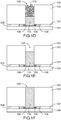
- Figures 1A to 1F represent the steps of a metallization method of a blind via 100 according to a first embodiment.
- the blind via 100 is made in a structure comprising a first substrate 102 secured to a second substrate 104 by a sealing interface 106.
- the first and second substrates 102 and 104 are for example based on silicon and each of thickness (dimension along the Z axis represented on the Figure 1A ) equal to about 720 ⁇ m.
- the via 100 has for example a section, in the plane (X, Y) and at the first substrate 102, substantially disk-shaped and of diameter for example equal to about 100 microns.
- the via 100 passes through the first substrate 102 and is thus opening at both an upper face 103 of the first substrate 102 and a lower face 105 of the first substrate 102.
- a bottom wall of the via blind 100 is formed. by a portion of an upper face 107 of the second substrate 104 which faces the void space formed by the via 100 in the first substrate 102.
- An electrical contact 108 for example based on an electrically conductive material such as only metal (for example gold) is disposed at this bottom wall of the via 100.
- electrical contacts 109 are also present in the via 100, at the lower face 105 of the first substrate 102.
- microelectronic devices are made on the first substrate 102 and / or the second substrate 104 and are electrically connected to the electrical contacts 108 and 109. In a variant, they are t also possible that electrical contacts are also at the level of the upper face 103 of the substrate 102, at the periphery of the via 100.
- a plurality of microbeads 110 based on an electrically conductive material are arranged in the blind via 100.
- the microbeads 110 are for example first disposed on the upper face 103 of the first substrate 102, then brought into the via 100 via a squeegee, for example similar to a squeegee used to implement a screen printing, which is brought the microbeads 110 in the blind via 100.
- the blind via 100 is filled by the microbeads 110.
- the electrically conductive material of the microbeads 110 is here a fusible alloy, for example an alloy based on tin, silver and copper.
- the electrically conductive material used may be chosen for example depending on the material of the substrate 102 and / or the material of the electrical contacts intended to be in contact with the metallization material (the electrical contacts 108 and 109 in this first embodiment), and for example based on copper and / or gold and / or nickel. Care will be taken to choose, for the microbeads 110, a material whose melting point is lower than that of the materials of the other elements, in particular contacts electric.
- the diameters of the microbeads 110 are smaller than that of the blind via 100.
- microbeads 110 all have a substantially similar diameter. However, it is possible to fill the blind via 100 with microbeads 110 of different diameters, which can increase the filling compactness of the blind via 100, that is to say, to reduce the empty space unoccupied by the microbeads 110 in the blind via 100 when it is filled by the microbeads 110.
- the value indicated in the "maximum diameter” column corresponds to the maximum diameter that a microbead of the type in question can have.
- the value in the “Nominal Diameter” column is the maximum diameter that up to 1% of the microbeads of this type can have.
- the range of values indicated in the column “Range of diameters” corresponds to the range of diameters of at least 90% of the microbeads of the type in question.
- microbeads 110 By making the microbeads 110 from nanoparticles of alloy, it is possible to make microbeads of diameter even smaller than those indicated in the table above. In addition, there is no technological limit on the maximum possible size of microbeads 110.
- the assembly in which the blind via 100 is carried out that is to say the substrates 102, 104, is then subjected to heat treatment in order to melt the microbeads 110.
- the temperature necessary for melting the microbeads depends the melting temperature of the material of the microbeads 110.
- the table below indicates the liquidus temperatures of alloys that can be used to make the microbeads 110.
- the electrically conductive material of the microbeads 110 By melting the electrically conductive material of the microbeads 110, the latter flows to the bottom of the blind via 100. However, since empty spaces are present between the microbeads 110 when they are arranged in the blind via 100, the air under the microbeads 110 can escape through these empty spaces, which allows to metallize the blind via 100 without forming air bubbles under the metallization. As shown on the figure 1C the molten material of the microbeads 110 is then cooled, forming a portion 112 of solidified electrically conductive material which corresponds to a part of the metallization of the blind via 100. This portion 112 is in contact with the electrical contacts 108 and 109.
- An empty space 111 is present in the blind via 100, above the portion 112 of solidified electrically conductive material, between the first portion 112 of the metallization and the opening of the blind via 100 located at the upper face 103 of the first substrate 102.
- This empty space 111 substantially corresponds to the empty spaces present between the microbeads 110 before they are melted.
- the operation is then repeated by filling the empty space 111 with microbeads 110, for example similar to those used during the previous filling of the blind via 100.
- a new heat treatment is then used to melt these microbeads 110.
- the resulting molten material then mixes with the material of the metallization portion 112 which also melts since it undergoes the same heat treatment as the microbeads 110.
- the microbeads 110 used during the various process steps all have a substantially similar diameter.
- microbeads of smaller and smaller sizes can be used during the process as the metallization part obtained after cooling approaches the upper face 103 of the second substrate 102.
- the microbeads arranged on the portion 112 could have a diameter smaller than that of the microbeads initially arranged in the blind via (those represented on the Figure 1A ).
- the second substrate 104 is secured to the first substrate 102 permanently via the sealing interface 106.
- the second substrate 104 is secured only to temporarily to the first substrate 102, the time that the vias are metallized. This second substrate would therefore be used to form temporary bottom walls of the vias 100.
- FIG. 3 represents a metallized blind via 300 according to a variant of the method previously described in connection with the Figures 1A to 1F .
- the one-eyed via 300 is formed by the first substrate 102, the second substrate 104 being connected to the first substrate 102 via the sealing interface 106.
- An electrical contact 108 is disposed at the bottom of the blind via 300.
- side walls 113 of the blind via 300 are previously treated in order to render them non-wetting with respect to the material of the microbeads 110.
- a treatment may consist in producing a deposition of fluorinated material, for example of the type CF 4 , C 4 F 8 , or CHF 3 , by plasma treatment, for example by PECVD, against the side walls 113 of the via blind 300.
- plasma treatment for example by PECVD
- Such a surface treatment forms a very thin deposit (a few atomic layers or a few nanometers) of fluorinated material against the walls 113.
- PDMS polydimethylsiloxane
- silicone or teflon type or a derivative of these components
- the space between the walls 113 of the blind via 300 and the portion of solidified electrically conductive material 115 can isolate laterally the electrical contact formed by the contact 108 connected to the conductive portion 115 of the substrate 102, without the need for prior electrical insulation.
- the free space between the walls 113 and the portion of solidified electrically conductive material 115 may be left as it is or filled, for example with the aid of an insulating polymer, for example benzocyclobutene, polyimide, etc.
- FIGS. 2A to 2D represent the steps of a method of metallization of blind vias 200 according to a second embodiment.
- blind vias 200 are made in a substrate 202, for example of similar nature and dimensions to those of the first substrate 102 previously described. However, unlike the via 100, the vias 200 do not pass through the substrate 202 and each comprise a single opening at an upper face 203 of the substrate 202. Electrical contacts 204 are also made on the upper face 203 of the substrate 202, at the periphery of the vias 200 openings.
- Another blind via 201 which does not wish to metallize at the same time as the blind vias 200, is also made in the substrate 202.
- Each of the blind vias 200 has side walls 206 and a bottom wall 208 formed in the substrate 202.
- the side walls 206 and the bottom walls 208 of the vias 200 are treated in such a way that make the material electrically wetting
- This treatment may for example consist of a deposition of a suitable material, for example an alloy of nickel and gold, on the side walls 206 and the bottom walls. 208 one-eyed vias 200.
- the mask 209 may for example comprise a sheet of stainless steel machined by laser and mechanically plated on the substrate 202, or comprise a substrate, for example based on silicon, previously etched by laser or by deep etching and mechanically plated on the substrate 102.
- Solid portions 210 of an electrically conductive material are then scattered over the mask 209.
- the solid portions 210 are not microbeads and form granules of random shapes.
- the substrate 202 is then vibrated so that desired amounts of solid portions 210 fall into the blind vias 200 to be metallized.
- the surplus of solid portions 210 still present on the substrate 200 is then removed, for example by realizing a gentle blowing on the mask 209 ( Figure 2B ).
- the mask 209 is then removed.
- a heat treatment is then carried out which melts the solid portions 210 of electrically conductive material. Due to the treatment previously carried out to make the side walls 206 and the bottom walls 208 wetting towards the material of the solid portions 210, the melted material of the solid portions 210 does not accumulate at the bottom of the vias 200 but comes wetting the side walls 206 and the bottom walls 208 of the blind vias 200. In cooling, the vias 200 are therefore metallized at their side walls 206 and their bottom wall 208 covered by a layer 212 of metallization based on electrically conductive material ( Figure 2C ).
- the electrical contacts 204 are arranged at the periphery of the openings of the vias 200 and the electrically conductive layers 212 go up to the level of the openings of the vias 200 at the upper face 203 of the substrate 202, electrical contacts are created between the metallization layers 212 and the electrical contacts 204 at each of the vias 200.
- the process is then completed by thinning the substrate 202 at a rear face 205 of the substrate 202, for example by implementing a chemical mechanical planarization with a stop on the metallization layer 212.
- the contacts electrical 204 are electrically accessible from a rear face 207 of the thinned substrate 202 through the metallization layers 212.
- the metallizations vias 200 obtained will be similar to those made for the vias 100, that is to say formed by portions of electrically conductive material completely or partially filling the space in the vias.
- the metallization of the vias may consist of firstly filling the vias with an electrically conductive material as shown in FIG. figure 1C and then to continue the metallization of the vias by forming an electrically conductive layer along the portions of the side walls of the vias located above the portions of electrically conductive material previously solidified in the vias.
- the metallization methods described above are particularly applicable to metallize blind vias formed in an imaging device, the vias may extend from the upper optical portion of the imager to the lower electronic portion. Thus, it is possible to take back electrical contacts of the electronic part from the optical part of the imager.
- the vias 100, 200 and 300 previously described all have a disk-shaped section, the previously described metallization process can be applied to vias of any shape and any size from the moment it It is possible to introduce at least one solid portion, also of any shape, of electrically conductive material into the blind via.
Landscapes
- Internal Circuitry In Semiconductor Integrated Circuit Devices (AREA)
- Printing Elements For Providing Electric Connections Between Printed Circuits (AREA)
Claims (10)
- Verfahren zur Metallisierung mindestens einer Blindloch-Durchkontaktierung (100, 200, 300), die in mindestens einem Substrat (102, 202) ausgebildet ist, wobei es zumindest die folgenden Schritte beinhaltet:a) Anordnen mindestens einer fest vorliegenden Portion (110, 210) von elektrisch leitendem Material in der Blindloch-Durchkontaktierung (100, 200, 300),b) Durchführen einer thermischen Behandlung der fest vorliegenden Portion (110, 210) von elektrisch leitendem Material, wodurch dieses in der Blindloch-Durchkontaktierung (100, 200, 300) zum Schmelzen gebracht wird,c) Durchführen einer Abkühlung des elektrisch leitenden Materials (112, 114, 115, 116, 212), wobei dieses in der Blindloch-Durchkontaktierung (100, 200, 300) verfestigt wird,dadurch gekennzeichnet, dass
vor der Durchführung von Schritt a) mindestens ein Teil der Wände (113) der Blindloch-Durchkontaktierung (300) mit einem Material überzogen wird, das geeignet ist, das Benetzen dieses Teils der Wände (113) der Blindloch-Durchkontaktierung (300) durch das geschmolzene elektrisch leitende Material zu verhindern, welches man während der Durchführung von Schritt b) erhält, wobei das verfestigte elektrisch leitende Material (115), das nach Durchführung von Schritt c) erhalten wird, mit diesen nicht-benetzenden Teil der Wände (113) der Blindloch-Durchkontaktierung (300) nicht fest verbunden ist,
und wobei das Material, das geeignet ist, das Benetzen des Teils der Wände der Blindloch-Durchkontaktierung (300) zu verhindern, mit dem geschmolzenen elektrisch leitenden Material einen Tropfen-Kontaktwinkel bildet, der ungefähr 180° beträgt, und/oder einem fluorierten Material entspricht oder PDMS, Silikon, Teflon oder ein Derivat dieser Bestandteile enthält. - Verfahren nach Anspruch 1, wobei die fest vorliegende Portion von elektrisch leitendem Material eine Mikrokugel (110) ist.
- Verfahren nach Anspruch 2, wobei vor Schritt a) die Mikrokugel (110) auf einer Fläche (103) des Substrats (102) angeordnet wird, bei der die Blindloch-Durchkontaktierung (100) mündet, und dann im Verlauf von Schritt a) in die Blindloch-Durchkontaktierung (100) hineingeschoben und/odergerollt wird.
- Verfahren nach Anspruch 1 oder 2, wobei vor Schritt a) die fest vorliegende Portion (210) von elektrisch leitendem Material auf einer Fläche (203) des Substrats (202) angeordnet wird, bei der die Blindloch-Durchkontaktierung (200) mündet, und wobei im Verlauf von Schritt a) die fest vorliegende Portion (210) von elektrisch leitendem Material in der Blindloch-Durchkontaktierung (200) durch In-Vibration-Versetzen des Substrats (202) angeordnet wird.
- Verfahren nach einem der vorhergehenden Ansprüche, wobei die Blindloch-Durchkontaktierung (100) durch das Substrat (102) hindurchgeht, das als erstes Substrat bezeichnet wird, derart, dass die Blindloch-Durchkontaktierung (100) bei zwei gegenüberliegenden Flächen (103, 105) des ersten Substrats (102) mündet, wobei eine Wand des Bodens der Blindloch-Durchkontaktierung (100) durch mindestens ein zweites Substrat (104) gebildet wird, das mit dem ersten Substrat (102) fest verbunden ist.
- Verfahren nach einem der vorhergehenden Ansprüche, wobei mindestens ein elektrischer Kontakt (108, 109, 204) im Wesentlichen bei einer Wandung des Bodens der Blindloch-Durchkontaktierung (100) und/oder auf mindestens einer Fläche (103, 105, 203) des Substrates (102, 202) angeordnet ist, bei der die Blindloch-Durchkontaktierung (100, 200) mündet, und zwar insgesamt oder teilweise am Umfang der Blindloch-Durchkontaktierung (100, 200), wobei das verfestigte elektrisch leitende Material (112, 114, 116, 212), das nach der Durchführung von Schritt c) erhalten wird, mit dem elektrischen Kontakt (108, 109, 204) elektrisch verbunden ist.
- Verfahren nach einem der vorhergehenden Ansprüche, wobei die Durchführung der Schritte a) bis c) mehrmals wiederholt wird, wodurch die Menge an verfestigtem elektrisch leitenden Material (114, 116) in der Blindloch-Durchkontaktierung (100) mit jeder weiteren Durchführung von Schritt c) bezüglich der Menge an verfestigtem elektrisch leitenden Material (112, 114), die bei einer vorhergehenden Durchführung von Schritt c) erzielt wurde, erhöht wird.
- Verfahren nach Anspruch 7, wobei bei einer nachmaligen Durchführung von Schritt a) die Abmessungen der verwendeten fest vorliegenden Portion (110) von elektrisch leitendem Material geringer als die Abmessungen der fest vorliegenden Portion (110) an elektrisch leitendem Material sind, die man bei einer vorhergehenden Durchführung von Schritt a) verwendet hat.
- Verfahren nach einem der vorhergehenden Ansprüche, wobei mittels der Durchführung der Schritte a) bis c) gleichzeitig die Metallisierung von mehreren Blindloch-Durchkontaktierungen (200), die zumindest in dem Substrat (202) ausgebildet sind, realisiert wird.
- Verfahren nach Anspruch 9, wobei vor der Durchführung von Schritt a) eine Maske (209) auf einer Fläche (203) des Substrates (202) angeordnet wird, bei der die Blindloch-Durchkontaktierungen (200) münden, wobei die Maske (209) mindestens eine Öffnung (211) aufweist, die mit mindestens einer der Blindloch-Durchkontaktierungen (200) fluchtet.
Applications Claiming Priority (1)
| Application Number | Priority Date | Filing Date | Title |
|---|---|---|---|
| FR1051726A FR2957480B1 (fr) | 2010-03-10 | 2010-03-10 | Procede de metallisation de vias borgnes |
Publications (2)
| Publication Number | Publication Date |
|---|---|
| EP2365741A1 EP2365741A1 (de) | 2011-09-14 |
| EP2365741B1 true EP2365741B1 (de) | 2018-09-19 |
Family
ID=42735458
Family Applications (1)
| Application Number | Title | Priority Date | Filing Date |
|---|---|---|---|
| EP11157121.2A Not-in-force EP2365741B1 (de) | 2010-03-10 | 2011-03-07 | Verfahren zur metallisierung von blindlöchern |
Country Status (3)
| Country | Link |
|---|---|
| US (1) | US9003654B2 (de) |
| EP (1) | EP2365741B1 (de) |
| FR (1) | FR2957480B1 (de) |
Families Citing this family (9)
| Publication number | Priority date | Publication date | Assignee | Title |
|---|---|---|---|---|
| WO2014194049A1 (en) | 2013-05-31 | 2014-12-04 | The Regents Of The University Of California | Through silicon vias and thermocompression bonding using inkjet-printed nanoparticles |
| WO2015082951A1 (en) | 2013-12-06 | 2015-06-11 | Commissariat à l'énergie atomique et aux énergies alternatives | Method of hermetically sealing a hole with a fuse material |
| CN104596925A (zh) * | 2015-01-22 | 2015-05-06 | 深圳崇达多层线路板有限公司 | 用于检测hdi板金属化盲孔底部与内层基铜结合力的方法 |
| CN105848428B (zh) * | 2016-04-22 | 2018-07-31 | 深圳崇达多层线路板有限公司 | 一种在pcb上制作金属化盲孔的方法 |
| EP3471132B1 (de) * | 2017-10-12 | 2020-02-26 | ams AG | Verfahren zur herstellung eines halbleiterbauelements sowie halbleiterbauelement |
| CN115565935B (zh) * | 2021-07-01 | 2026-04-28 | 长鑫存储技术有限公司 | 一种半导体器件的制作方法以及半导体器件 |
| CN113512743B (zh) * | 2021-09-14 | 2021-12-10 | 新恒汇电子股份有限公司 | 智能卡载带盲孔电镀方法 |
| CN116322279B (zh) | 2021-12-17 | 2024-10-22 | 腾讯科技(深圳)有限公司 | 硅片及其硅孔的填充方法 |
| CN118921887B (zh) * | 2024-07-11 | 2025-09-02 | 中国电子科技集团公司第二十九研究所 | 一种实现ltcc基板盲腔侧壁金属化的装置及其使用方法 |
Citations (2)
| Publication number | Priority date | Publication date | Assignee | Title |
|---|---|---|---|---|
| US20040261636A1 (en) * | 2002-05-17 | 2004-12-30 | Fry's Metals, Inc. D/B/A Alpha Metals, Inc. | Coated stencil with reduced surface tension |
| US20060008627A1 (en) * | 2004-07-09 | 2006-01-12 | Hewlett-Packard Development Company, L.P. | Laser enhanced plating |
Family Cites Families (7)
| Publication number | Priority date | Publication date | Assignee | Title |
|---|---|---|---|---|
| JP2002144523A (ja) | 2000-11-14 | 2002-05-21 | Matsushita Electric Ind Co Ltd | ブラインドビア用ペースト充填方法およびペースト充填装置 |
| JP2003092467A (ja) * | 2001-09-19 | 2003-03-28 | Tatsuta Electric Wire & Cable Co Ltd | プリント配線基板およびその製法 |
| KR20060034850A (ko) * | 2004-10-20 | 2006-04-26 | 삼성전자주식회사 | 배선 장치, 이를 이용한 디바이스 패키지용 보호 캡,그리고 그것들을 제조하기 위한 방법 |
| US7452568B2 (en) | 2005-02-04 | 2008-11-18 | International Business Machines Corporation | Centrifugal method for filing high aspect ratio blind micro vias with powdered materials for circuit formation |
| US7851342B2 (en) * | 2007-03-30 | 2010-12-14 | Intel Corporation | In-situ formation of conductive filling material in through-silicon via |
| JP5424632B2 (ja) * | 2008-12-19 | 2014-02-26 | キヤノン株式会社 | インクジェット記録ヘッド用基板の製造方法 |
| FR2951870B1 (fr) | 2009-10-28 | 2012-03-30 | Commissariat Energie Atomique | Structure d'interconnexion a cavite presentant une ou plusieurs remontees de contact sur les parois de la cavite et procede de realisation |
-
2010
- 2010-03-10 FR FR1051726A patent/FR2957480B1/fr not_active Expired - Fee Related
-
2011
- 2011-03-03 US US13/039,902 patent/US9003654B2/en active Active
- 2011-03-07 EP EP11157121.2A patent/EP2365741B1/de not_active Not-in-force
Patent Citations (2)
| Publication number | Priority date | Publication date | Assignee | Title |
|---|---|---|---|---|
| US20040261636A1 (en) * | 2002-05-17 | 2004-12-30 | Fry's Metals, Inc. D/B/A Alpha Metals, Inc. | Coated stencil with reduced surface tension |
| US20060008627A1 (en) * | 2004-07-09 | 2006-01-12 | Hewlett-Packard Development Company, L.P. | Laser enhanced plating |
Also Published As
| Publication number | Publication date |
|---|---|
| FR2957480A1 (fr) | 2011-09-16 |
| EP2365741A1 (de) | 2011-09-14 |
| US20110219612A1 (en) | 2011-09-15 |
| US9003654B2 (en) | 2015-04-14 |
| FR2957480B1 (fr) | 2012-08-31 |
Similar Documents
| Publication | Publication Date | Title |
|---|---|---|
| EP2365741B1 (de) | Verfahren zur metallisierung von blindlöchern | |
| EP2053646B1 (de) | Verfahren zur vertikalen Verbindung durch Vias in dreidimensionallen elektronischen Modulen | |
| EP2192612B1 (de) | Verfahren zum Stapeln und Vernetzen von integrierten Schaltkreisen | |
| EP2816624B1 (de) | Verfahren zur Herstellung einer Substratdurchkontaktierung und eines durchgehenden Kondensators in einem Substrat | |
| EP2175485B1 (de) | Lötverbindung zwischen zwei ineinandergreifenden Steckern, und Verfahren zur deren Herstellung | |
| FR2992467A1 (fr) | Procede de realisation d'un composant a contact electrique traversant et composant obtenu | |
| WO2013001225A1 (fr) | Composant de connexion muni d'inserts creux | |
| EP2608253A2 (de) | Silizium-Durchkontaktierungspunkt (TSV) einer Struktur zur Freisetzung von Stress, und entsprechendes Herstellungsverfahren | |
| EP2126969A1 (de) | Verfahren zur verbindung elektronischer wafer | |
| EP3651195B1 (de) | Herstellungsverfahren eines kühlkreislaufs | |
| EP2791969B1 (de) | Herstellung einer elektrischen durchgangsverbindung | |
| EP2690655B1 (de) | Verfahren zur Herstellung von Durchkontaktierungen | |
| EP2543625B1 (de) | Verfahren zur Herstellung eines eingebetteten Metallteils in einer Uhr | |
| EP3772746B1 (de) | Verfahren zur herstellung von durchgangsverbindungen durch ein substrat | |
| FR2958076A1 (fr) | Procede de formation de vias electriques | |
| EP2365743B1 (de) | Verbindungsstruktur, die Sacklöcher umfasst, die metallisiert werden sollen | |
| WO2025103976A1 (fr) | Procédé de réalisation d'un dispositif comprenant des pistes affleurantes | |
| EP4513268A1 (de) | Verfahren zur herstellung von mustern auf einem substrat | |
| EP4513269A1 (de) | Verfahren zur strukturierung eines substrats | |
| FR2923080A1 (fr) | Procede de fabrication d'un via dans une plaquette de semi-conducteur | |
| FR3078821A1 (fr) | Procede de realisation d'une bille de brasure sur une face d'un substrat | |
| FR2855323A1 (fr) | Procede de realisation d'un circuit electronique integre comprenant un condensateur | |
| FR3045943A1 (fr) | Dispositif semi-conducteur et procede pour realiser un contact a travers le substrat semi-conducteur |
Legal Events
| Date | Code | Title | Description |
|---|---|---|---|
| PUAI | Public reference made under article 153(3) epc to a published international application that has entered the european phase |
Free format text: ORIGINAL CODE: 0009012 |
|
| AK | Designated contracting states |
Kind code of ref document: A1 Designated state(s): AL AT BE BG CH CY CZ DE DK EE ES FI FR GB GR HR HU IE IS IT LI LT LU LV MC MK MT NL NO PL PT RO RS SE SI SK SM TR |
|
| AX | Request for extension of the european patent |
Extension state: BA ME |
|
| 17P | Request for examination filed |
Effective date: 20120313 |
|
| 17Q | First examination report despatched |
Effective date: 20160129 |
|
| STAA | Information on the status of an ep patent application or granted ep patent |
Free format text: STATUS: EXAMINATION IS IN PROGRESS |
|
| RIC1 | Information provided on ipc code assigned before grant |
Ipc: H05K 3/34 20060101AFI20180226BHEP Ipc: H01L 21/768 20060101ALI20180226BHEP Ipc: H01L 21/683 20060101ALI20180226BHEP Ipc: H01L 23/00 20060101ALI20180226BHEP |
|
| GRAP | Despatch of communication of intention to grant a patent |
Free format text: ORIGINAL CODE: EPIDOSNIGR1 |
|
| STAA | Information on the status of an ep patent application or granted ep patent |
Free format text: STATUS: GRANT OF PATENT IS INTENDED |
|
| INTG | Intention to grant announced |
Effective date: 20180417 |
|
| RIN1 | Information on inventor provided before grant (corrected) |
Inventor name: BOLIS, SEBASTIEN Inventor name: JACUET, FABRICE Inventor name: SAINT-PATRICE, DAMIEN |
|
| GRAS | Grant fee paid |
Free format text: ORIGINAL CODE: EPIDOSNIGR3 |
|
| GRAA | (expected) grant |
Free format text: ORIGINAL CODE: 0009210 |
|
| STAA | Information on the status of an ep patent application or granted ep patent |
Free format text: STATUS: THE PATENT HAS BEEN GRANTED |
|
| AK | Designated contracting states |
Kind code of ref document: B1 Designated state(s): AL AT BE BG CH CY CZ DE DK EE ES FI FR GB GR HR HU IE IS IT LI LT LU LV MC MK MT NL NO PL PT RO RS SE SI SK SM TR |
|
| REG | Reference to a national code |
Ref country code: GB Ref legal event code: FG4D Free format text: NOT ENGLISH |
|
| REG | Reference to a national code |
Ref country code: CH Ref legal event code: EP |
|
| REG | Reference to a national code |
Ref country code: DE Ref legal event code: R096 Ref document number: 602011052119 Country of ref document: DE |
|
| REG | Reference to a national code |
Ref country code: AT Ref legal event code: REF Ref document number: 1044870 Country of ref document: AT Kind code of ref document: T Effective date: 20181015 |
|
| REG | Reference to a national code |
Ref country code: IE Ref legal event code: FG4D Free format text: LANGUAGE OF EP DOCUMENT: FRENCH |
|
| REG | Reference to a national code |
Ref country code: NL Ref legal event code: MP Effective date: 20180919 |
|
| PG25 | Lapsed in a contracting state [announced via postgrant information from national office to epo] |
Ref country code: NO Free format text: LAPSE BECAUSE OF FAILURE TO SUBMIT A TRANSLATION OF THE DESCRIPTION OR TO PAY THE FEE WITHIN THE PRESCRIBED TIME-LIMIT Effective date: 20181219 Ref country code: BG Free format text: LAPSE BECAUSE OF FAILURE TO SUBMIT A TRANSLATION OF THE DESCRIPTION OR TO PAY THE FEE WITHIN THE PRESCRIBED TIME-LIMIT Effective date: 20181219 Ref country code: GR Free format text: LAPSE BECAUSE OF FAILURE TO SUBMIT A TRANSLATION OF THE DESCRIPTION OR TO PAY THE FEE WITHIN THE PRESCRIBED TIME-LIMIT Effective date: 20181220 Ref country code: LT Free format text: LAPSE BECAUSE OF FAILURE TO SUBMIT A TRANSLATION OF THE DESCRIPTION OR TO PAY THE FEE WITHIN THE PRESCRIBED TIME-LIMIT Effective date: 20180919 Ref country code: FI Free format text: LAPSE BECAUSE OF FAILURE TO SUBMIT A TRANSLATION OF THE DESCRIPTION OR TO PAY THE FEE WITHIN THE PRESCRIBED TIME-LIMIT Effective date: 20180919 Ref country code: RS Free format text: LAPSE BECAUSE OF FAILURE TO SUBMIT A TRANSLATION OF THE DESCRIPTION OR TO PAY THE FEE WITHIN THE PRESCRIBED TIME-LIMIT Effective date: 20180919 Ref country code: SE Free format text: LAPSE BECAUSE OF FAILURE TO SUBMIT A TRANSLATION OF THE DESCRIPTION OR TO PAY THE FEE WITHIN THE PRESCRIBED TIME-LIMIT Effective date: 20180919 |
|
| REG | Reference to a national code |
Ref country code: LT Ref legal event code: MG4D |
|
| PG25 | Lapsed in a contracting state [announced via postgrant information from national office to epo] |
Ref country code: AL Free format text: LAPSE BECAUSE OF FAILURE TO SUBMIT A TRANSLATION OF THE DESCRIPTION OR TO PAY THE FEE WITHIN THE PRESCRIBED TIME-LIMIT Effective date: 20180919 Ref country code: LV Free format text: LAPSE BECAUSE OF FAILURE TO SUBMIT A TRANSLATION OF THE DESCRIPTION OR TO PAY THE FEE WITHIN THE PRESCRIBED TIME-LIMIT Effective date: 20180919 Ref country code: HR Free format text: LAPSE BECAUSE OF FAILURE TO SUBMIT A TRANSLATION OF THE DESCRIPTION OR TO PAY THE FEE WITHIN THE PRESCRIBED TIME-LIMIT Effective date: 20180919 |
|
| REG | Reference to a national code |
Ref country code: AT Ref legal event code: MK05 Ref document number: 1044870 Country of ref document: AT Kind code of ref document: T Effective date: 20180919 |
|
| PG25 | Lapsed in a contracting state [announced via postgrant information from national office to epo] |
Ref country code: IS Free format text: LAPSE BECAUSE OF FAILURE TO SUBMIT A TRANSLATION OF THE DESCRIPTION OR TO PAY THE FEE WITHIN THE PRESCRIBED TIME-LIMIT Effective date: 20190119 Ref country code: AT Free format text: LAPSE BECAUSE OF FAILURE TO SUBMIT A TRANSLATION OF THE DESCRIPTION OR TO PAY THE FEE WITHIN THE PRESCRIBED TIME-LIMIT Effective date: 20180919 Ref country code: EE Free format text: LAPSE BECAUSE OF FAILURE TO SUBMIT A TRANSLATION OF THE DESCRIPTION OR TO PAY THE FEE WITHIN THE PRESCRIBED TIME-LIMIT Effective date: 20180919 Ref country code: PL Free format text: LAPSE BECAUSE OF FAILURE TO SUBMIT A TRANSLATION OF THE DESCRIPTION OR TO PAY THE FEE WITHIN THE PRESCRIBED TIME-LIMIT Effective date: 20180919 Ref country code: IT Free format text: LAPSE BECAUSE OF FAILURE TO SUBMIT A TRANSLATION OF THE DESCRIPTION OR TO PAY THE FEE WITHIN THE PRESCRIBED TIME-LIMIT Effective date: 20180919 Ref country code: ES Free format text: LAPSE BECAUSE OF FAILURE TO SUBMIT A TRANSLATION OF THE DESCRIPTION OR TO PAY THE FEE WITHIN THE PRESCRIBED TIME-LIMIT Effective date: 20180919 Ref country code: RO Free format text: LAPSE BECAUSE OF FAILURE TO SUBMIT A TRANSLATION OF THE DESCRIPTION OR TO PAY THE FEE WITHIN THE PRESCRIBED TIME-LIMIT Effective date: 20180919 Ref country code: CZ Free format text: LAPSE BECAUSE OF FAILURE TO SUBMIT A TRANSLATION OF THE DESCRIPTION OR TO PAY THE FEE WITHIN THE PRESCRIBED TIME-LIMIT Effective date: 20180919 Ref country code: NL Free format text: LAPSE BECAUSE OF FAILURE TO SUBMIT A TRANSLATION OF THE DESCRIPTION OR TO PAY THE FEE WITHIN THE PRESCRIBED TIME-LIMIT Effective date: 20180919 |
|
| PG25 | Lapsed in a contracting state [announced via postgrant information from national office to epo] |
Ref country code: SM Free format text: LAPSE BECAUSE OF FAILURE TO SUBMIT A TRANSLATION OF THE DESCRIPTION OR TO PAY THE FEE WITHIN THE PRESCRIBED TIME-LIMIT Effective date: 20180919 Ref country code: PT Free format text: LAPSE BECAUSE OF FAILURE TO SUBMIT A TRANSLATION OF THE DESCRIPTION OR TO PAY THE FEE WITHIN THE PRESCRIBED TIME-LIMIT Effective date: 20190119 Ref country code: SK Free format text: LAPSE BECAUSE OF FAILURE TO SUBMIT A TRANSLATION OF THE DESCRIPTION OR TO PAY THE FEE WITHIN THE PRESCRIBED TIME-LIMIT Effective date: 20180919 |
|
| REG | Reference to a national code |
Ref country code: DE Ref legal event code: R097 Ref document number: 602011052119 Country of ref document: DE |
|
| PLBE | No opposition filed within time limit |
Free format text: ORIGINAL CODE: 0009261 |
|
| STAA | Information on the status of an ep patent application or granted ep patent |
Free format text: STATUS: NO OPPOSITION FILED WITHIN TIME LIMIT |
|
| PG25 | Lapsed in a contracting state [announced via postgrant information from national office to epo] |
Ref country code: DK Free format text: LAPSE BECAUSE OF FAILURE TO SUBMIT A TRANSLATION OF THE DESCRIPTION OR TO PAY THE FEE WITHIN THE PRESCRIBED TIME-LIMIT Effective date: 20180919 |
|
| 26N | No opposition filed |
Effective date: 20190620 |
|
| PG25 | Lapsed in a contracting state [announced via postgrant information from national office to epo] |
Ref country code: MC Free format text: LAPSE BECAUSE OF FAILURE TO SUBMIT A TRANSLATION OF THE DESCRIPTION OR TO PAY THE FEE WITHIN THE PRESCRIBED TIME-LIMIT Effective date: 20180919 Ref country code: SI Free format text: LAPSE BECAUSE OF FAILURE TO SUBMIT A TRANSLATION OF THE DESCRIPTION OR TO PAY THE FEE WITHIN THE PRESCRIBED TIME-LIMIT Effective date: 20180919 |
|
| REG | Reference to a national code |
Ref country code: CH Ref legal event code: PL |
|
| PG25 | Lapsed in a contracting state [announced via postgrant information from national office to epo] |
Ref country code: LU Free format text: LAPSE BECAUSE OF NON-PAYMENT OF DUE FEES Effective date: 20190307 |
|
| REG | Reference to a national code |
Ref country code: BE Ref legal event code: MM Effective date: 20190331 |
|
| PG25 | Lapsed in a contracting state [announced via postgrant information from national office to epo] |
Ref country code: IE Free format text: LAPSE BECAUSE OF NON-PAYMENT OF DUE FEES Effective date: 20190307 Ref country code: CH Free format text: LAPSE BECAUSE OF NON-PAYMENT OF DUE FEES Effective date: 20190331 Ref country code: LI Free format text: LAPSE BECAUSE OF NON-PAYMENT OF DUE FEES Effective date: 20190331 |
|
| PG25 | Lapsed in a contracting state [announced via postgrant information from national office to epo] |
Ref country code: BE Free format text: LAPSE BECAUSE OF NON-PAYMENT OF DUE FEES Effective date: 20190331 |
|
| PG25 | Lapsed in a contracting state [announced via postgrant information from national office to epo] |
Ref country code: TR Free format text: LAPSE BECAUSE OF FAILURE TO SUBMIT A TRANSLATION OF THE DESCRIPTION OR TO PAY THE FEE WITHIN THE PRESCRIBED TIME-LIMIT Effective date: 20180919 |
|
| PG25 | Lapsed in a contracting state [announced via postgrant information from national office to epo] |
Ref country code: MT Free format text: LAPSE BECAUSE OF FAILURE TO SUBMIT A TRANSLATION OF THE DESCRIPTION OR TO PAY THE FEE WITHIN THE PRESCRIBED TIME-LIMIT Effective date: 20180919 |
|
| PG25 | Lapsed in a contracting state [announced via postgrant information from national office to epo] |
Ref country code: CY Free format text: LAPSE BECAUSE OF FAILURE TO SUBMIT A TRANSLATION OF THE DESCRIPTION OR TO PAY THE FEE WITHIN THE PRESCRIBED TIME-LIMIT Effective date: 20180919 |
|
| PG25 | Lapsed in a contracting state [announced via postgrant information from national office to epo] |
Ref country code: HU Free format text: LAPSE BECAUSE OF FAILURE TO SUBMIT A TRANSLATION OF THE DESCRIPTION OR TO PAY THE FEE WITHIN THE PRESCRIBED TIME-LIMIT; INVALID AB INITIO Effective date: 20110307 |
|
| PG25 | Lapsed in a contracting state [announced via postgrant information from national office to epo] |
Ref country code: MK Free format text: LAPSE BECAUSE OF FAILURE TO SUBMIT A TRANSLATION OF THE DESCRIPTION OR TO PAY THE FEE WITHIN THE PRESCRIBED TIME-LIMIT Effective date: 20180919 |
|
| PGFP | Annual fee paid to national office [announced via postgrant information from national office to epo] |
Ref country code: DE Payment date: 20240321 Year of fee payment: 14 Ref country code: GB Payment date: 20240318 Year of fee payment: 14 |
|
| PGFP | Annual fee paid to national office [announced via postgrant information from national office to epo] |
Ref country code: FR Payment date: 20240320 Year of fee payment: 14 |
|
| REG | Reference to a national code |
Ref country code: DE Ref legal event code: R119 Ref document number: 602011052119 Country of ref document: DE |
|
| GBPC | Gb: european patent ceased through non-payment of renewal fee |
Effective date: 20250307 |
|
| PG25 | Lapsed in a contracting state [announced via postgrant information from national office to epo] |
Ref country code: DE Free format text: LAPSE BECAUSE OF NON-PAYMENT OF DUE FEES Effective date: 20251001 |
|
| PG25 | Lapsed in a contracting state [announced via postgrant information from national office to epo] |
Ref country code: GB Free format text: LAPSE BECAUSE OF NON-PAYMENT OF DUE FEES Effective date: 20250307 |
|
| PG25 | Lapsed in a contracting state [announced via postgrant information from national office to epo] |
Ref country code: FR Free format text: LAPSE BECAUSE OF NON-PAYMENT OF DUE FEES Effective date: 20250331 |