EP2368965A2 - Fluoreszenzstoff, Verfahren zur Herstellung und von dem Stoff gebrauch machende Leuchtvorrichtung - Google Patents
Fluoreszenzstoff, Verfahren zur Herstellung und von dem Stoff gebrauch machende Leuchtvorrichtung Download PDFInfo
- Publication number
- EP2368965A2 EP2368965A2 EP10251563A EP10251563A EP2368965A2 EP 2368965 A2 EP2368965 A2 EP 2368965A2 EP 10251563 A EP10251563 A EP 10251563A EP 10251563 A EP10251563 A EP 10251563A EP 2368965 A2 EP2368965 A2 EP 2368965A2
- Authority
- EP
- European Patent Office
- Prior art keywords
- light
- fluorescent substance
- wavelength range
- emitting
- peak
- Prior art date
- Legal status (The legal status is an assumption and is not a legal conclusion. Google has not performed a legal analysis and makes no representation as to the accuracy of the status listed.)
- Withdrawn
Links
Images


Classifications
-
- C—CHEMISTRY; METALLURGY
- C09—DYES; PAINTS; POLISHES; NATURAL RESINS; ADHESIVES; COMPOSITIONS NOT OTHERWISE PROVIDED FOR; APPLICATIONS OF MATERIALS NOT OTHERWISE PROVIDED FOR
- C09K—MATERIALS FOR MISCELLANEOUS APPLICATIONS, NOT PROVIDED FOR ELSEWHERE
- C09K11/00—Luminescent materials, e.g. electroluminescent or chemiluminescent
- C09K11/08—Luminescent materials, e.g. electroluminescent or chemiluminescent containing inorganic luminescent materials
- C09K11/77—Luminescent materials, e.g. electroluminescent or chemiluminescent containing inorganic luminescent materials containing rare earth metals
- C09K11/7728—Luminescent materials, e.g. electroluminescent or chemiluminescent containing inorganic luminescent materials containing rare earth metals containing europium
- C09K11/77348—Silicon Aluminium Nitrides or Silicon Aluminium Oxynitrides
-
- H—ELECTRICITY
- H10—SEMICONDUCTOR DEVICES; ELECTRIC SOLID-STATE DEVICES NOT OTHERWISE PROVIDED FOR
- H10H—INORGANIC LIGHT-EMITTING SEMICONDUCTOR DEVICES HAVING POTENTIAL BARRIERS
- H10H20/00—Individual inorganic light-emitting semiconductor devices having potential barriers, e.g. light-emitting diodes [LED]
- H10H20/80—Constructional details
- H10H20/85—Packages
- H10H20/851—Wavelength conversion means
- H10H20/8511—Wavelength conversion means characterised by their material, e.g. binder
- H10H20/8512—Wavelength conversion materials
- H10H20/8513—Wavelength conversion materials having two or more wavelength conversion materials
-
- H—ELECTRICITY
- H10—SEMICONDUCTOR DEVICES; ELECTRIC SOLID-STATE DEVICES NOT OTHERWISE PROVIDED FOR
- H10W—GENERIC PACKAGES, INTERCONNECTIONS, CONNECTORS OR OTHER CONSTRUCTIONAL DETAILS OF DEVICES COVERED BY CLASS H10
- H10W72/00—Interconnections or connectors in packages
- H10W72/50—Bond wires
- H10W72/551—Materials of bond wires
- H10W72/552—Materials of bond wires comprising metals or metalloids, e.g. silver
- H10W72/5522—Materials of bond wires comprising metals or metalloids, e.g. silver comprising gold [Au]
Definitions
- the embodiment relates to a fluorescent substance, a process for production of the fluorescent substance, a light-emitting device and a light-emitting module.
- LED lamps which utilize light-emitting diodes, are used in many displaying elements of instruments such as mobile devices, PC peripheral equipments, OA equipments, various kinds of switches, light sources for backlighting, and indicating boards.
- the LED lamps are strongly required not only to have high efficiency, but also to be excellent in color rendition when used for general lighting or to deliver a wide color gamut when used for backlighting.
- it is necessary to improve fluorescent substances used in light-emitting parts of LEDs For example, in order to increase the efficiency of lamps, it is necessary to adopt highly efficient fluorescent substances in the LEDs. Further, for improving the color rendition and for broadening the color gamut of lamps, it is desired to improve chromaticity of luminescence emitted from the fluorescent substances.
- high load LEDs generally become so hot while working that fluorescent substances used therein are heated up to a temperature of approx. 100 to 200°C.
- their emission intensity is generally lowered. Accordingly, it is desired that the emission intensity be less lowered even if the fluorescent substances are heated. In other words, it is desired that the temperature quenching be less induced.
- red SiAlON phosphors comprising mainly silicon and aluminum
- Those phosphors are, for example, represented by the formula of (Sr 1-x EU x ) a Si b Al c O d N e , and they are improved in temperature quenching as compared with conventional phosphors such as Sr 2 Si 5 N 8 : Eu and CaS:Eu.
- One aspect of the embodiment resides in a process for production of a fluorescent substance which emits luminescence having a peak in the wavelength range of 570 to 650 nm under excitation by light in the wavelength range of 250 to 500 nm, comprising the step of:
- Another aspect of the embodiment resides in a first fluorescent substance which emits luminescence having a peak in the wavelength range of 570 to 650 nm under excitation by light in the wavelength range of 250 to 500 nm and which is obtained by mixing
- a light-emitting device comprises
- a light-emitting device comprises
- a light-emitting device module comprises a substrate and plural light-emitting devices provided thereon, each of said light-emitting devices comprising:
- a light-emitting device module comprises a substrate and plural light-emitting devices provided thereon, each of said light-emitting devices comprising:
- the process of the embodiment for production of red fluorescent substance is characterized by adopting a compound containing In(III) or Ga(III) as a material.
- the oxynitride fluorescent substance according to the embodiment is what is called a SiAlON phosphor, which has a matrix comprising: Si or a tetravalent metal element replacing Si, Al or a trivalent metal element replacing Al, oxide and nitrogen.
- the oxynitride fluorescent substance can be produced by the steps of: mixing compounds containing the above elements to prepare a material mixture, and then firing the mixture.
- the material mixture includes a compound containing In(III) or Ga(III).
- the following (1) to (5) are materials used in the process of the embodiment for production of the oxynitride fluorescent substance. Those are,
- the metal element M 1 contained in the material (1) is Si or an element replacing Si, and it constitutes a SiAlON phosphor intended to be formed by the embodiment and is selected from the group consisting of tetravalent metal elements.
- the tetravalent metal element M 1 is preferably selected from the IVA and IVB groups, and examples thereof include Si, Ge, Sn, Ti, Zr and Hf.
- Si is particularly preferred.
- the metal element M 1 may be either a single element or a combination of two or more elements.
- the compound of M 1 is preferably a nitride, oxide or carbide.
- the metal element M 2 contained in the material (2) is Al or an element replacing Al, and it constitutes a SiAlON phosphor intended to be formed by the embodiment and is selected from the group consisting of trivalent metal elements.
- the trivalent metal element M 2 is preferably selected from the IIIA and IIIB groups, and examples thereof include Al, B, Sc, Y, La, Gd and Lu.
- Al is particularly preferred.
- the metal element M 2 is neither In(III) nor Ga(III).
- the metal element M 2 may be either a single element or a combination of two or more elements.
- the compound of M 2 is preferably a nitride, oxide or carbide.
- the metal element M contained in the material (3) is selected from the group consisting of metal elements other than the above M 1 , M 2 , In(III) and Ga(III).
- the metal element M is preferably selected from the IA (alkali metal) group elements such as Li, Na and K; the IIA (alkaline earth metal) group elements such as Mg, Ca, Sr and Ba; the IIIA group elements such as B; the IIIB group elements such as Y and Sc; the rare earth elements such as Gd, La and Lu; or the IVA group elements such as Ge.
- the metal element M Sr is particularly preferred.
- the metal element M may be either a single element or a combination of two or more elements.
- the compound containing the element M is preferably a nitride or carbide such as cyanamide.
- the metal element M in the fluorescent substance of the embodiment is so selected as to be different from the elements M 1 and M 2 .
- the metal element EC contained in the material (4) serves as an emission center of the fluorescent substance.
- the fluorescent substance according to the embodiment has a crystal structure basically comprising the elements M, M 1 , M 2 and O and/or N, but the metal element M is partly replaced with the emission center element EC.
- Examples of the emission center element EC include Eu, Ce, Mn, Tb, Yb, Dy, Sm, Tm, Pr, Nd, Pm, Ho, Er, Cr, Sn, Cu, Zn, As, Ag, Cd, Sb, Au, Hg, Tl, Pb, Bi and Fe.
- Eu and Mn can be preferably selected in consideration of emission wavelength variability and the like.
- the compound containing the metal element EC is preferably an oxide, nitride or carbonate.
- the material (5) is a compound containing In(III) or Ga(III).
- the compound include oxides and nitrides such as In 2 O 3 , Ga 2 O 3 and GaN.
- the mixing ratio of the materials can be adequately controlled according to what composition the oxynitride fluorescent substance is intended to have.
- the oxynitride fluorescent substance intended to be produced by the process of the embodiment emits luminescence having a peak in the wavelength range of 570 to 650 nm when excited by light in the wavelength range of 250 to 500 nm.
- the fluorescent substance giving that emission basically has a crystal structure of M 2 M 1 7 M 2 3 ON 13 , but the metal element M is partly replaced with the emission center element EC. Accordingly, the materials are generally so mixed that the molar ratio among the total amount of M and EC, the amount of M 1 and the amount of M 2 may be about 2:7:3. However, this value does not need to be kept strictly because the molar ratio can be controlled in view of the peak wavelength of the luminescence or the like.
- 0.1 mol% or more of the metal element M is replaced with the emission center element EC. If the amount of the replaced M is less than 0.1 mol%, it is difficult to obtain sufficient emission intensity.
- the metal element M can be completely replaced with the emission center element EC. However, if the amount of the replaced M is less than 50 mol%, the decrease of emission probability (concentration quenching) can be prevented to the utmost.
- the red fluorescent substance of the embodiment emits light in the range of yellow to red, namely, gives off luminescence having a peak in the wavelength range of 570 to 650 nm when excited by light of 250 to 500 nm.
- the process of the embodiment for production of fluorescent substance is characterized by using the material (5) (i.e., compound containing the metal element L). It is indispensable in the embodiment to adopt the material (5) together with other materials, but this does not necessarily mean that the oxynitride fluorescent substance contains the metal element L. For example, if the material (5) is used in a relatively large amount, the element L is often found in analysis of the obtained oxynitride fluorescent substance. Accordingly, in the resultant fluorescent substance, the element L may replace the metal M 1 or the like.
- the material (5) is used in such a small amount that the element L in the resultant oxynitride fluorescent substance is in an amount below the measurement limit of the analysis, the effect of the embodiment is sometimes clearly observed.
- the material (5) is incorporated into the crystal of the fluorescent substance but also it may control the crystal growth thereof.
- the material (5) added in the firing step may form a liquid or gas phase capable of providing some function for crystal growth during the firing step and, as a result, may give the effect of the embodiment.
- the fluorescent substance produced by the process of the embodiment has luminescence properties different from conventional red fluorescent substances containing Sr.
- the obtained fluorescent substance less comprises hetero-phases giving blue to green luminescence and exhibits an emission spectrum having a smaller half-width. Consequently, the fluorescent substance according to the embodiment is improved in chromaticity as compared with known Sr-containing red fluorescent substances.
- the fluorescent substance of the embodiment is in the form of larger grains than conventional Sr-containing red fluorescent substances, and accordingly is presumed to have absorption efficiency high enough to improve the emission efficiency.
- Those advantages of the fluorescent substance according to the embodiment are thought to be given by the material (5) during crystal growth.
- the metal element L in the material (5) does not always take the place of the trivalent metal element M 2 included in the crystal structure of the fluorescent substance. Accordingly, it is not necessarily reasonable to regulate the amount of the material (5) based on that of M 2 .
- the amount of L contained in the material (5) is regulated as follows on the basis of the amount of M 2 contained in the material (3); that is, the amount of L is preferably 0.1 to 50 mol%, more preferably 0.1 to 20 mol%, based on the amount of M 2 . If the metal element L is much contained, the hetero-phases are liable to increase in producing the fluorescent substance so that the yield thereof may be lowered. This should be noted.
- the process of the embodiment for production of red light-emitting fluorescent substance comprises the steps of: mixing the aforementioned materials in a desired ratio; pulverizing and mixing the mixture, generally, in a mortar; and then firing the mixture.
- Sr, Eu, Si, Al and In are selected as the elements M, EC, M 1 , M 2 and L, respectively.
- Sr 3 N 2 , AIN, Si 3 N 4 , Al 2 O 3 , In 2 O 3 and EuN as the starting materials.
- Sr 2 N, SrN or mixtures thereof in place of Sr 3 N 2 .
- In 2 O 3 may be replaced with other In compounds.
- the materials are weighed and mixed so that the aimed composition can be obtained, and the prepared powdery mixture is then fired in a crucible to produce the aimed fluorescent substance.
- the materials are mixed, for example, in a mortar in a glove box.
- the crucible is made of, for example, boron nitride, silicon nitride, silicon carbide, carbon, aluminum nitride, SiAlON, aluminum oxide, molybdenum or tungsten.
- the process for production of the oxynitride fluorescent substance comprises the step of firing the mixture of the starting materials for a predetermined time.
- the firing is preferably carried out under a pressure more than the atmospheric pressure.
- the pressure is preferably not less than 5 atmospheres.
- the firing temperature is preferably in the range of 1500 to 2000°C, more preferably in the range of 1800 to 2000°C. If the temperature is less than 1500°C, it is often difficult to obtain the aimed fluorescent substance. On the other hand, if the temperature is more than 2000°C, there is a fear that the materials or the product may be sublimated.
- the firing is preferably carried out under N 2 atmosphere. In that case, N 2/ H 2 mixed gas atmosphere is also usable.
- the fired product in the form of powder is then subjected to after-treatment such as washing, if necessary, to obtain a fluorescent substance according to the embodiment. If performed, washing can be carried out with acid or pure water.
- a first red light-emitting fluorescent substance according to the embodiment is produced by the above-described process. Specifically, that is an oxynitride fluorescent substance which emits luminescence having a peak in the wavelength range of 570 to 650 nm under excitation by light in the wavelength range of 250 to 500 nm and which is obtained by firing the above materials (1) to (4) in the presence of the material (5).
- the crystal structure of fluorescent substance can be identified by X-ray diffraction or neutron diffraction.
- the red light-emitting fluorescent substance of the embodiment preferably has a crystal structure exhibiting the XRD profile same as Sr 2 Al 3 Si 7 ON 13 , and it is also preferred to have a crystal structure in which the constituting elements of Sr 2 Al 3 Si 7 ON 13 are replaced with other elements so as to change the lattice constants within particular ranges.
- Figure 1 is an XRD profile of the basic Sr 2 Al 3 Si 7 ON 13. The constituting elements of Sr 2 Al 3 Si 7 ON 13 are replaced with other elements in such a way described below in detail.
- Sr in the crystal is replaced with the element M and/or the emission center element EC;
- the site of Si is filled with one or more elements selected from the group consisting of tetravalent elements such as Ge, Sn, Ti, Zr and Hf;
- the site of Al is filled with one or more elements selected from the group consisting of trivalent elements such as B, Sc, Y, La, Gd and Lu;
- the site of O or N is filled with one or more elements selected from the group consisting of O N and C.
- Al and Si may be partly substituted with each other, and O and N may be partly substituted with each other.
- Examples of that substance include Sr 2 Al 2 Si 8 N 14 , Sr 2 Al 4 Si 6 O 2 N 12 , Sr 2 Al 15 Si 5 O 3 N 11 and Sr 2 Al 6 Si 4 O 4 N 10 . These substances have crystal structures based on Sr 2 Al 3 Si 7 ON 13.
- the crystal is slightly fused, it can be judged whether or not the fused crystal has a structure based on Sr 2 Al 3 Si 7 ON 13 by the following simple method.
- the XRD profile of the modified crystal is measured, and the positions of the diffraction peaks are compared with those in the XRD profile of Sr 2 Al 3 Si 7 ON 13 .
- the main peaks for comparison it is preferred to select 10 peaks having strong diffraction intensity.
- a second red light-emitting fluorescent substance according to the embodiment is represented by the following formula (I): (M 1 - x EC x)a M 1 b M 2 L c O d N e (I).
- M 1 is a metal element selected from the group consisting of tetravalent metal elements
- M 2 is a metal element selected from the group consisting of trivalent metal elements other than In(III) and Ga(III)
- L is a metal element selected from the group consisting of In(III) and Ga(III)
- M is a metal element selected from the group consisting of metal elements other than M 1 , M 2 , In(III) and Ga(III)
- EC is an emission center element other than any of the aforesaid metal elements
- x, a, b, c, d and e are numbers satisfying the conditions of 0 ⁇ x ⁇ 0.4, 0.65 ⁇ a ⁇ 0.80, 2 ⁇ b ⁇ 3, 0 ⁇ c ⁇ 0.1, 0.3 ⁇ d ⁇ 0.6 and 4 ⁇ e ⁇ 5, respectively.
- the numbers preferably satisfy the conditions of 0.02 ⁇ x ⁇ 0.2, 0.66 ⁇ a ⁇ 0.73, 2.2 ⁇ b ⁇ 2.7, 0 ⁇ c ⁇ 0.05, 0.35 ⁇ d ⁇ 0.49 and 4.2 ⁇ e ⁇ 4.7, respectively
- the composition ratio of the metal element L is more than 0 in the above, and this does not mean that the content of the element L is below the measurement limit of analyzing apparatus. Specifically, even if the element L is not detected when the fluorescent substance is analyzed by means of an apparatus having the highest detection sensitivity at present, the technology may become so improved that the element L will be detected in the future. In that case, such fluorescent substance is included in the second fluorescent substance according to the embodiment. Further, even in the case where the content of the element L is still below the measurement limit, such fluorescent substance is obviously included in the first fluorescent substance according to the embodiment, provided that the material (5) is used in the production process thereof.
- composition of oxynitride fluorescent substance can be analyzed in any known manner, for example, in the following manner.
- the contents of M, M 1 , M 2 and EC can be measured by, for example, inductively coupled plasma atomic emission spectroscopic analysis (often referred to as "ICY analysis"). Specifically, the sample of oxynitride fluorescent substance is weighed in a platinum crucible and then decomposed by alkali fusion. After an internal standard element Y is added, the decomposed sample is dissolved to prepare a sample solution, which is subsequently subjected to ICP analysis. The analysis can be carried out by means of, for example, an ICP emission spectrometry (SPS-4000 [trademark], manufactured by SII Nano Technology Inc.).
- SPS-4000 ICP emission spectrometry
- the contents of O and N can be measured, for example, by the inert gas fusion method.
- the sample of oxynitride fluorescent substance is heated to melt in a graphite crucible, and O atoms contained in the sample are converted into CO with inert gas transfer.
- the CO is further oxidized into CO 2 which is then measured by IR absorption spectroscopy to determine the content of O.
- the content of N is measured by the heat conduction method.
- the measurement can be carried out by means of, for example, an oxygen, nitrogen-hydrogen analyzer (TC-600 [trademark], manufactured by LECO corporation (US)).
- the content of In can be measured by ICP analysis. Specifically, the sample of oxynitride fluorescent substance is weighed in a pressure decomposition vessel, and then acid-decomposed under pressure to prepare a sample solution, which is subsequently subjected to ICP analysis.
- the analysis can be carried out by means of, for example, an ICP emission spectrometry (SPQ-9000 [trademark], manufactured by SII Nano Technology Inc.).
- the content of Ga can be also measured by ICP analysis.
- a sample solution is prepared in the same manner as the measurement of the element M, and then subjected to ICP analysis by means of, for example, an ICP emission spectrometry (SPS-1500V [trademark], manufactured by SII Nano Technology Inc.).
- a light-emitting device comprises the above red light-emitting fluorescent substance and a light-emitting element capable of exciting the fluorescent substance.
- the device comprises: a light-emitting element, such as a LED, serving as an excitation source; and a combination of the aforementioned red fluorescent substance (R) and a green fluorescent substance (G) each of which emits luminescence under excitation by light given off from the light-emitting element. Accordingly, the light-emitting device radiates light synthesized with emissions from the light-emitting element and the red and green fluorescent substances.
- a light-emitting element such as a LED, serving as an excitation source
- a combination of the aforementioned red fluorescent substance (R) and a green fluorescent substance (G) each of which emits luminescence under excitation by light given off from the light-emitting element. Accordingly, the light-emitting device radiates light synthesized with emissions from the light-emitting element and the red and green fluorescent substances.
- the light-emitting device comprises: a light-emitting element serving as an excitation source; and a combination of the above red fluorescent substance (R), the above green fluorescent substance (G) and a blue fluorescent substance (B) each of which emits luminescence under excitation by light given off from the light-emitting element.
- the light-emitting device can adopt either of the first and second fluorescent substances of the embodiment.
- the light-emitting element used in the device is properly selected according to the fluorescent substances used together. Specifically, it is necessary that light given off from the light-emitting element be capable of exciting the fluorescent substances. Further, if the device is preferred to radiate white light, the light-emitting element preferably gives off light of such a wavelength that it can complement luminescence emitted from the fluorescent substances.
- the light-emitting element (S1) is generally so selected that it gives off light in the wavelength range of 250 to 500 nm. If the device comprises the red, green and blue fluorescent substances, the light-emitting element (S2) is generally so selected that it gives off light of 250 to 430 nm.
- the light-emitting device according to the embodiment can be in the form of any conventionally known light-emitting device.
- Figure 2 is a vertical sectional view schematically illustrating a package cup-type light-emitting device of the embodiment.
- a resin stem 200 comprises leads 201 and 202 molded as parts of a lead frame and also a resin member 203 formed by unified molding together with the lead frame.
- the resin member 203 gives a concavity 205 in which the top opening is larger than the bottom.
- a reflective surface 204 is provided on the inside wall of the concavity.
- a light-emitting element 206 is mounted with Ag paste or the like.
- the light-emitting element 206 include a light-emitting diode and a laser diode.
- the light-emitting element may radiate UV light.
- a semiconductor light-emitting element such as GaN can be used as the light-emitting element.
- the electrodes (not shown) of the light-emitting element 206 are connected to the leads 201 and 202 by way of bonding wires 207 and 208 made of Au or the like, respectively. The positions of the leads 201 and 202 can be adequately modified.
- a phosphor layer 209 is provided in the concavity 205 of the resin member 203.
- a fluorescent substance 210 of the embodiment can be dispersed or precipitated in a resin layer 211 made of silicone resin or the like in an amount of 5 to 50 wt%.
- the fluorescent substance of the embodiment comprises an oxynitride matrix having high covalency, and hence is generally so hydrophobic that it has good compatibility with the resin. Accordingly, scattering at the interface between the resin and the fluorescent substance is prevented enough to improve the light-extraction efficiency.
- the light-emitting element 206 may be of a flip chip type in which n-type and p-type electrodes are placed on the same plane. This element can avoid troubles concerning the wires, such as disconnection or dislocation of the wires and light-absorption by the wires. In that case, therefore, a semiconductor light-emitting device excellent both in reliability and in luminance can be obtained. Further, it is also possible to employ an n-type substrate in the light-emitting element 206 so as to produce a light-emitting device constituted as described below. In that device, an n-type electrode is formed on the back surface of the n-type substrate while a p-type electrode is formed on the top surface of the semiconductor layer on the substrate.
- One of the n-type and p-type electrodes is mounted on one of the leads, and the other electrode is connected to the other lead by way of a wire.
- the size of the light-emitting element 206 and the dimension and shape of the concavity 205 can be properly changed.
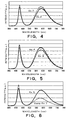
- FIG. 3 illustrates schematic vertical sectional views of shell-type light-emitting devices according to another embodiment.
- a diode 301 emitting light having an emission peak at, for example, 445 nm is soldered on a package substrate 302 made of AIN and the like, and is connected to an electrode by way of an electroconductive wire 303.
- the light-emitting diode 301 is domed with a transparent resin layer 304 made of silicone resin or the like, and thereon a transparent resin layer 305 containing the red light-emitting fluorescent substance, a transparent resin layer 306 and a transparent resin layer 307 containing the green light-emitting fluorescent substance are stacked in order.
- the device of Figure 3A thus comprises the light-emitting element and the red and green light-emitting fluorescent substances each of which gives off luminescence under excitation by light emitted from the diode.
- the device can be further provided with a layer of blue light-emitting fluorescent substance.
- Figure 3B shows a schematic vertical sectional view of such device, which further comprises a transparent resin layer 308 and a layer 309 containing the blue light-emitting fluorescent substance. Those layers are formed on the green fluorescent substance layer 307 of the device shown in Figure 3A .
- the light-emitting diode used in the device of Figure 3B is generally designed to radiate light containing blue component in a less amount than that in the device of Figure 3A . This is because the excitation light and the luminescence emitted from each fluorescent substance are so designed that the light-emitting device can give off light of desired color, such as while light, in total.
- the light-emitting device according to the embodiment is not restricted to the package cup-type and the shell-type shown in Figures 2 and 3 , respectively, and can be freely applied to any type of devices. For example, even if the fluorescent substance according to the embodiment is used in a surface-mount type light-emitting device, the same effect can be obtained.
- a light-emitting device module comprises a plural number of the aforementioned light-emitting devices arranged on a substrate. Any of the above light-emitting devices, which comprise the fluorescent substance of the embodiment, can be freely selected to be used in the module.
- the shell-type device described above is one of those preferably employed in the module.
- the light-emitting device module comprises a plural number of any of the following light-emitting devices:
- materials of the substrate there is no particular restriction on materials of the substrate, and hence it can be freely selected from known materials according to the aim.
- examples of the materials include glass, silicone, semiconductors and resins.
- the surface of the substrate may be subjected to various modifications according to necessity. For example, wiring or isolation structures for the light-emitting devices can be laid on the surface. Further, in order to improve heat-dissipating, a heat-sinking layer can be formed thereon.
- the substrate in itself may be a heat-sinking substrate excellent in thermal conductivity.
- the green fluorescent substance emit luminescence having a peak in the wavelength range of 490 to 580 nm when excited by light given off from the light-emitting element (S1) or (S2), and the blue fluorescent substance emit luminescence having a peak in the wavelength range of 400 to 490 nm when excited by light given off from the light-emitting element (S1) or (S2).
- the light-emitting devices are regularly or irregularly arranged on the substrate to form a light-emitting device module. Since having excellent temperature characteristics, the fluorescent substance of the embodiment is hardly affected by heat generated in operation. Accordingly, the devices comprising the fluorescent substances can be arranged so densely that the interval among them can be shortened.
- the aforementioned shell-type devices seem to be circles or ellipses when seen from above, and they can be placed in such an arrangement as satisfies the condition of 1 ⁇ (d/a) ⁇ 5 in which "a" and "d" are the major axis length of the ellipses and the shortest distance among them, respectively.
- the "major axis length” here means the longest diameter of the horizontal section of each light-emitting device.
- each light-emitting device has a circular or elliptical horizontal section, it means its diameter or its major axis length, respectively.
- the light-emitting devices can have sections in any shapes, such as rectangles, polygons or lines. In that case, the interval among them cannot be uniformly regulated. Even so, however, the interval among them can be shortened enough to enhance the luminance of the whole light-emitting device module. That is because the fluorescent substance of the embodiment is so excellent in temperature characteristics that its luminescence is hardly affected by heat generated by the adjacent light-emitting devices in operation.
- red light-emitting fluorescent substance of the embodiment It is indispensable to employ a red light-emitting fluorescent substance of the embodiment in a light-emitting device or a light-emitting device module according to the embodiment.
- the red fluorescent substance (R) of the embodiment has such excellent temperature characteristics that it is hardly affected by temperature change.
- both the green fluorescent substance (G) and the blue one (B) are preferably excellent in temperature characteristics, too.
- the light-emitting device or module gives off light less changed in color even when the temperature is changed. That is not only because the red fluorescent substance emits luminescence less changed in intensity but also because the other fluorescent substances emit luminescence less changed in intensity, too.
- the light-emitting device or module is particularly suitable for working under a high temperature condition.
- One of the green fluorescent substances (G) preferably used in the light-emitting device or module of the embodiment belongs among SiAlON phosphors like the above red fluorescent substance does, but the basic crystal structure thereof is different from that of the red fluorescent substance.
- the green fluorescent substance (G) is based on Sr 3 Si 13 Al 3 O 2 N 21 , which belongs to an orthorhombic system.
- the constituting elements thereof are partly replaced with light-emitting elements like those of the red fluorescent substance are.
- the modification such as replacement may slightly change the crystal structure, but the effect of the embodiment can be obtained provided that the basic crystal structure is not essentially changed. To what extent the basic crystal structure is not changed is the same as that of the red fluorescent substance.
- the green fluorescent substance can be identified by X-ray diffraction or neutron diffraction.
- the green fluorescent substance includes not only a fluorescent substance exhibiting the XRD profile same as Sr 3 Si 13 Al 3 O 2 N 21 , but also a substance in which the constituting elements of Sr 3 Si 13 Al 3 O 2 N 21 are replaced with other elements so as to change the lattice constants within particular ranges.
- the light-emitting device or module according to the embodiment also preferably comprises a blue fluorescent substance excellent in temperature characteristics.
- the preferred blue fluorescent substance include (Ba,Eu)MgAl 10 O 17 , (SrCa,Ba,Eu) 10 (PO 4 ) 5 Cl 2 and (Sr,Eu)Si 9 Al 19 ON 31.
- Sr 3 N 2 , EuN, Si 3 N 4 , Al 2 O 3 , AlN and Ga 2 O 3 in the amounts of 2.308 g, 0.697 g, 4.583 g, 0.454 g, 1.339 g and 0.039 g, respectively, were weighed and dry-mixed in an agate mortar in a vacuum glove box. The mixture was placed in a BN crucible and then fired at 1850°C for 4 hours under 7.5 atm of N 2 atmosphere, to synthesize a fluorescent substance.
- Example 1 The procedure of Example 1 was repeated except that the amounts of Al 2 O 3 and Ga 2 O 3 were changed into 0.262 g and 0.394 g, respectively, to synthesize a fluorescent substance.
- Sr 3 N 2 , EuN, Si 3 N 4 , Al 2 O 3 , AIN and GaN in the amounts of 2.308 g, 0.697 g, 4.583 g, 0.476 g, 1.322 g and 0.035 g, respectively, were weighed and dry-mixed in an agate mortar in a vacuum glove box. The mixture was placed in a BN crucible and then fired at 1850°C for 4 hours under 7.5 atm of N 2 atmosphere, to synthesize a fluorescent substance.
- Example 3 The procedure of Example 3 was repeated except that the amounts of AlN and GaN were changed into 1.167 g and 0.352 g, respectively, to synthesize a fluorescent substance.
- Example 1 The procedure of Example 1 was repeated except that Sr 3 N 2 , EuN, Si 3 N 4 , Al 2 O 3 and AlN were used in the amounts of 2.308 g, 0.697 g, 4.583 g, 0.476 g and 1.339 g, respectively, to synthesize a fluorescent substance whose designed composition was (Sr 0.85 Eu 0.15 ) 2 Al 3 Si 7 ON 13.
- Comparative Example 1 The procedure of Comparative Example 1 was repeated except that the amounts of Sr 3 N 2 and EuN were changed into 2.443 g and 0.465 g, respectively, to synthesize a fluorescent substance whose designed composition was (Sr 0.9 Eu 0.1 ) 2 Al 3 Si 7 ON 13 .
- Comparative Example 1 The procedure of Comparative Example 1 was repeated except that the amounts of Sr 3 N 2 and EuN were changed into 2.172 g and 0.929 g, respectively, to synthesize a fluorescent substance whose designed composition was (Sr 0.8 EU 0.2 ) 2 Al 3 Si 7 ON 13.
- Comparative Example 1 The procedure of Comparative Example 1 was repeated except that the amounts of Sr 3 N 2 and EuN were changed into 1.629 g and 1.859 g, respectively, to synthesize a fluorescent substance whose designed composition was (Sr 0.6 Eu 0.4 ) 2 Al 3 Si 7 ON 13 .
- Comparative Example 1 The procedure of Comparative Example 1 was repeated except that the amounts of Sr 3 N 2 and EuN were changed into 1.357 g and 2.324 g, respectively, to synthesize a fluorescent substance whose designed composition was (Sr 0.5 Eu 0.5 ) 2 Al 3 Si 7 ON 13 .
- Comparative Example 1 The procedure of Comparative Example 1 was repeated except that the amounts of Sr 3 N 2 and EuN were changed into 0.543 g and 3.718 g, respectively, to synthesize a fluorescent substance whose designed composition was (Sr 0.2 Eu 0.8 ) 2 Al 3 Si 7 ON 13 .
- Sr 3 N 2 , EuN, Si 3 N 4 , Al 2 O 3 , AlN and In 2 O 3 in the amounts of 2.308 g, 0.697 g, 4.583 g, 0.262 g, 1.339 g and 0.583 g, respectively, were weighed and dry-mixed in an agate mortar in a vacuum glove box. The mixture was placed in a BN crucible and then fired at 1850°C for 4 hours under 7.5 atm of N 2 atmosphere, to synthesize a fluorescent substance.
- Example 5 The procedure of Example 5 was repeated except that 0.583 g of In 2 O 3 was replaced with 0.290 g of SC 2 O 3 , to synthesize a fluorescent substance.
- the fluorescent substances of Examples 1 to 5 were subjected to composition analysis, and the results were as set forth in Table 1.
- the composition ratios in Table 1 were normalized by regarding the content of Al as 1.
- the feed ratio of Al:Ga in the materials of Example 1 or 3 was 99:1, that of Al:Ga in the materials of Example 2 or 4 was 90:10, and that of AI:IN in the materials of Example 5 was 90:10.
- all the resultant fluorescent substances contained them in ratios different from the feed ratios, and it was found that each fluorescent substance contained In or Ga in an amount smaller than the added amount.
- Table 1 Sr Eu Al Si O N Ga In Ex. 1 0.58 0.10 1 2.33 0.40 4.22 0.00043 - Ex. 2 0.62 0.11 1 2.51 0.40 4.45 0.00150 - Ex. 3 0.58 0.10 1 2.38 0.47 4.33 0.00062 - Ex. 4 0.60 0.11 1 2.50 0.46 4.50 0.00083 - Ex. 5 0.61 0.11 1 2.50 0.38 4.63 - 0.0000037
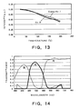
- the red powdery substances of Examples 1 to 5 and Comparative Example 7 were pulverized and then excited with a LED light source emitting light having a peak at 458 nm.
- the obtained emission spectra were shown in Figures 4 to 6 .
- the peak at 458 nm was attributed to the reflection of the excitation light.
- each of the red powdery substances of Examples 1 to 5 showed a single emission band having a peak in the wavelength range of 615 to 620 nm.
- that of Comparative Example 7 showed a single emission band having a peak in the wavelength range 610 to 615 nm.
- the red powder of Comparative Example 7 emitted luminescence having remarkably weaker intensity than that of Example 5, and accordingly was regarded as an inferior fluorescent substance.
- the effect of the embodiment can be obtained if a compound containing Ga or In is used as the material in producing the fluorescent substance, the effect cannot be obtained if the compound containing Ga or In is replaced with a compound containing Sc.
- Table 2 shows their chromaticity coordinates (x, y) in the CIE1931 chromaticity diagram.
- Table 2 chromaticity coordinate (CIE1931) Cx Cy Ex.1 0.57 0.41 Ex. 2 0.58 0.41 Ex. 3 0.57 0.41 Ex. 4 0.58 0.42 Ex. 5 0.59 0.41 Com. 1 0.54 0.41
- the red powdery substances of Example 3 and Comparative Example 1 were excited while they were being heated with a heater from room temperature to 200°C, to measure the change of the emission spectra.
- the light source used for excitation was a LED emitting light having a peak at 458 nm.
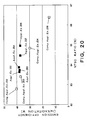
- the results were shown in Figure 13 , which indicates temperature dependence of the peak intensities of the emission spectra.
- the relative intensity plotted on the y-axis in Figure 13 was normalized under the condition that the intensity of each fluorescent substance at room temperature was regarded as 1.00.
- Figure 13 shows that the red fluorescent substance of Example 3 had temperature characteristics as excellent as Comparative Example 1.
- a light-emitting device of Application Example 101 was produced by use of the fluorescent substance synthesized in Example 1.
- the device had a structure according to Figure 3A .
- a LED 301 emitting light having a peak at 440 nm was soldered on an 8 mm-square AlN package substrate 302, and was connected to electrodes by way of gold wires 303.
- the LED was then domed with transparent resin 304, and the dome was coated with a layer of transparent resin 305 containing the red fluorescent substance of Example 1.
- another layer of transparent resin 306 and still another layer of transparent resin 307 containing a green fluorescent substance emitting luminescence having a peak at 520 nm were stacked thereon in order, to produce a light-emitting device.
- a light-emitting device module of Application Example 151 was produced by use of the fluorescent substance synthesized in Example 1.
- Figure 16 is a conceptual sketch showing the light-emitting device module of Application Example 151.
- This module comprised a heat-sinking substrate 1601 and plural shell-type light-emitting devices 1600 arranged thereon. Each shell-type light-emitting device had a structure shown in Figure 3A .
- the light-emitting device module was produced in the following manner. First, sixteen LEDs 301 emitting light having a peak at 440 nm were prepared, and they were placed and soldered on the heat-sinking substrate 1601 in such an arrangement that the center-to-center interval among them might be 6 mm.
- each LED soldered on the substrate was connected to electrodes by way of gold wires 303.
- Each LED was then domed with transparent resin 304, and the dome was coated with a layer of transparent resin 305 containing the red fluorescent substance of Example 1.
- another layer of transparent resin 306 and still another layer of transparent resin 307 containing a green fluorescent substance emitting luminescence having a peak at 520 nm were stacked thereon in order, to produce a light-emitting device module.
- Each device seemed to be a circle when seen from above, and its diameter was 2.8 mm.
- Table 3 and Figure 17 show the emission efficiency and the NTSC ratio (i.e., value in the u'-v' chromaticity coordinate system on the CIE1976 chromaticity diagram) measured through a diffuser and color filters.
- Table 3 NTSC ratio (%) Emission efficiency of white light source [Im/ W] (luminous efficacy) Ap. Ex.151 90.4 121 Ap. Ex.152 91.2 118 Ap. Ex.153 90.5 120 Ap. Ex.154 90.7 121 Ap. Ex.155 91.2 120 Com. Ap. 152 89.3 125 Com. Ap. 153 90.2 116 Com. Ap. 154 91.6 94 Com. Ap. 155 91.7 89 Com. Ap. 156 93.1 47
- a light-emitting device of Application Example 201 was produced by use of the fluorescent substance synthesized in Example 1.
- the device had a structure according to Figure 3B .
- a LED 301 emitting light having a peak at 390 nm was soldered on an 8 mm-square AlN package substrate 302, and was connected to electrodes by way of gold wires 303.
- the LED was then domed with transparent resin 304, and the dome was coated with a layer of transparent resin 305 containing the red fluorescent substance of Example 1.
- another layer of transparent resin 306 still another layer of transparent resin 307 containing a green fluorescent substance emitting luminescence having a peak at 520 nm, yet another layer of transparent resin 308 and still yet another layer of transparent resin 309 containing a blue fluorescent substance emitting luminescence having a peak at 452 nm were stacked thereon in order, to produce a light-emitting device.
- a light-emitting device module of Application Example 251 was produced by use of the fluorescent substance synthesized in Example 1.
- Figure 19 is a conceptual sketch showing the light-emitting device module of Application Example 251.
- This module comprised a heat-sinking substrate 1901 and plural shell-type light-emitting devices 1900 arranged thereon. Each shell-type light-emitting device had a structure shown in Figure 3B .
- the light-emitting device module was produced in the following manner. First, sixteen LEDs 301 emitting light having a peak at 390 nm were prepared, and they were placed and soldered on the heat-sinking substrate 1901 in such an arrangement that the center-to-center interval among them might be 6 mm.
- each LED soldered on the substrate was connected to electrodes by way of gold wires 303.
- Each LED was then domed with transparent resin 304, and the dome was coated with a layer of transparent resin 305 containing the red fluorescent substance of Example 1.
- another layer of transparent resin 306, still another layer of transparent resin 307 containing a green fluorescent substance emitting luminescence having a peak at 520 nm, yet another layer of transparent resin 308 and still yet another layer of transparent resin 309 containing a blue fluorescent substance emitting luminescence having a peak at 452 nm were stacked thereon in order, to produce a light-emitting device module.
- Each device seemed to be a circle when seen from above, and its diameter was 3.0 mm.
- Table 4 and Figure 20 show the emission efficiency and the NTSC ratio (i.e., value in the u'-v' chromaticity coordinate system on the CIE1976 chromaticity diagram) measured through a diffuser and color filters.
- Table 4 NTSC ratio (%) Emission efficiency of white light source [Im/ W] (luminous efficacy) Ap. Ex.251 82.8 40.3 Ap. Ex.252 83.4 37.1 Ap. Ex.253 84.8 29.7 Ap. Ex.254 86.4 14.6 Ap. Ex.255 83.7 38.0 Com. Ap.252 84.5 37.3 Com. Ap. 253 83.7 37.8 Com. Ap. 254 83.9 38.2 Com. Ap. 256 85.0 37.3
Landscapes
- Chemical & Material Sciences (AREA)
- Inorganic Chemistry (AREA)
- Engineering & Computer Science (AREA)
- Materials Engineering (AREA)
- Organic Chemistry (AREA)
- Luminescent Compositions (AREA)
- Led Device Packages (AREA)
Applications Claiming Priority (1)
| Application Number | Priority Date | Filing Date | Title |
|---|---|---|---|
| JP2010051630A JP5129283B2 (ja) | 2010-03-09 | 2010-03-09 | 蛍光体、蛍光体の製造方法、発光装置及び発光モジュール |
Publications (2)
| Publication Number | Publication Date |
|---|---|
| EP2368965A2 true EP2368965A2 (de) | 2011-09-28 |
| EP2368965A3 EP2368965A3 (de) | 2011-10-26 |
Family
ID=42942169
Family Applications (1)
| Application Number | Title | Priority Date | Filing Date |
|---|---|---|---|
| EP10251563A Withdrawn EP2368965A3 (de) | 2010-03-09 | 2010-09-08 | Fluoreszenzstoff, Verfahren zur Herstellung und von dem Stoff gebrauch machende Leuchtvorrichtung |
Country Status (6)
| Country | Link |
|---|---|
| US (1) | US8552437B2 (de) |
| EP (1) | EP2368965A3 (de) |
| JP (1) | JP5129283B2 (de) |
| KR (1) | KR101246511B1 (de) |
| CN (1) | CN102191058B (de) |
| TW (1) | TWI490310B (de) |
Cited By (4)
| Publication number | Priority date | Publication date | Assignee | Title |
|---|---|---|---|---|
| EP2426187A3 (de) * | 2010-09-02 | 2012-06-27 | Kabushiki Kaisha Toshiba | Fluoreszente Substanz und lichtemittierende Vorrichtung damit |
| KR20140054305A (ko) * | 2012-03-16 | 2014-05-08 | 가부시끼가이샤 도시바 | 형광체, 형광체의 제조 방법 및 발광 장치 |
| RU2641282C2 (ru) * | 2012-05-22 | 2018-01-16 | Люмиледс Холдинг Б.В. | Новые люминофоры, такие как новые узкополосные люминофоры красного свечения, для твердотельного источника света |
| RU2683077C2 (ru) * | 2013-09-26 | 2019-03-26 | Люмиледс Холдинг Б.В. | Новое люминесцирующее вещество на основе нитридоалюмосиликата для твердотельного освещения |
Families Citing this family (14)
| Publication number | Priority date | Publication date | Assignee | Title |
|---|---|---|---|---|
| JP5129392B2 (ja) * | 2009-08-28 | 2013-01-30 | 株式会社東芝 | 蛍光体の製造方法およびそれにより製造された蛍光体 |
| JP5076017B2 (ja) | 2010-08-23 | 2012-11-21 | 株式会社東芝 | 発光装置 |
| JP4991958B2 (ja) | 2010-09-06 | 2012-08-08 | 株式会社東芝 | 発光装置 |
| JP5185421B2 (ja) | 2010-09-09 | 2013-04-17 | 株式会社東芝 | 赤色発光蛍光体およびそれを用いた発光装置 |
| JP5865688B2 (ja) * | 2011-12-07 | 2016-02-17 | 株式会社東芝 | 蛍光体およびそれを用いた発光装置 |
| JP5749201B2 (ja) * | 2012-03-09 | 2015-07-15 | 株式会社東芝 | 白色発光装置 |
| KR20140121432A (ko) * | 2012-03-16 | 2014-10-15 | 가부시끼가이샤 도시바 | 형광체, 형광체의 제조 방법 및 발광 장치 |
| CN104024375B (zh) * | 2012-05-31 | 2017-05-24 | 国立研究开发法人物质·材料研究机构 | 荧光体及其制备方法、发光装置及图像显示装置 |
| DE102012210083A1 (de) * | 2012-06-15 | 2013-12-19 | Osram Gmbh | Optoelektronisches halbleiterbauelement |
| JP5646567B2 (ja) * | 2012-09-18 | 2014-12-24 | 株式会社東芝 | 蛍光体の製造方法 |
| JP2015176960A (ja) * | 2014-03-14 | 2015-10-05 | 株式会社東芝 | 発光装置 |
| CN105060328A (zh) * | 2015-08-04 | 2015-11-18 | 贵州远盛钾业科技有限公司 | 一种利用含钾岩石生产硫酸铝钾的方法 |
| JP6212589B2 (ja) * | 2016-03-28 | 2017-10-11 | シャープ株式会社 | 発光装置および画像表示装置 |
| JP2024124622A (ja) * | 2023-03-03 | 2024-09-13 | シチズン電子株式会社 | 発光装置 |
Citations (1)
| Publication number | Priority date | Publication date | Assignee | Title |
|---|---|---|---|---|
| WO2007105631A1 (ja) | 2006-03-10 | 2007-09-20 | Kabushiki Kaisha Toshiba | 蛍光体および発光装置 |
Family Cites Families (11)
| Publication number | Priority date | Publication date | Assignee | Title |
|---|---|---|---|---|
| DE10133352A1 (de) | 2001-07-16 | 2003-02-06 | Patent Treuhand Ges Fuer Elektrische Gluehlampen Mbh | Beleuchtungseinheit mit mindestens einer LED als Lichtquelle |
| JP4568867B2 (ja) | 2004-06-29 | 2010-10-27 | 独立行政法人物質・材料研究機構 | 複合窒化物蛍光体の製造方法 |
| US7439668B2 (en) | 2005-03-01 | 2008-10-21 | Lumination Llc | Oxynitride phosphors for use in lighting applications having improved color quality |
| CN102827603A (zh) * | 2005-03-04 | 2012-12-19 | 三菱化学株式会社 | 荧光体及其制备方法、和使用该荧光体的发光装置 |
| JP4975269B2 (ja) | 2005-04-28 | 2012-07-11 | Dowaホールディングス株式会社 | 蛍光体およびその製造方法、並びに当該蛍光体を用いた発光装置 |
| ATE492141T1 (de) | 2005-06-30 | 2011-01-15 | Koninkl Philips Electronics Nv | Beleuchtungssystem mit einem gelbes und grünes licht emittierenden leuchtstoff |
| US20070052342A1 (en) * | 2005-09-01 | 2007-03-08 | Sharp Kabushiki Kaisha | Light-emitting device |
| CN102816565B (zh) * | 2005-09-27 | 2015-05-27 | 三菱化学株式会社 | 荧光体及其制造方法、以及使用该荧光体的发光装置 |
| BRPI0807118A2 (pt) | 2007-02-06 | 2014-04-08 | Koninkl Philips Electronics Nv | Material, uso de um material, dispositivo de emissão de luz, e, sistema. |
| CN101157854B (zh) * | 2007-07-02 | 2010-10-13 | 北京宇极科技发展有限公司 | 一种氮氧化合物发光材料、其制备方法及其应用 |
| JP4869317B2 (ja) | 2008-10-29 | 2012-02-08 | 株式会社東芝 | 赤色蛍光体およびそれを用いた発光装置 |
-
2010
- 2010-03-09 JP JP2010051630A patent/JP5129283B2/ja active Active
- 2010-09-03 US US12/875,507 patent/US8552437B2/en active Active
- 2010-09-06 TW TW099130061A patent/TWI490310B/zh not_active IP Right Cessation
- 2010-09-07 CN CN201010277528.5A patent/CN102191058B/zh not_active Expired - Fee Related
- 2010-09-08 EP EP10251563A patent/EP2368965A3/de not_active Withdrawn
- 2010-09-20 KR KR1020100092279A patent/KR101246511B1/ko active Active
Patent Citations (1)
| Publication number | Priority date | Publication date | Assignee | Title |
|---|---|---|---|---|
| WO2007105631A1 (ja) | 2006-03-10 | 2007-09-20 | Kabushiki Kaisha Toshiba | 蛍光体および発光装置 |
Cited By (7)
| Publication number | Priority date | Publication date | Assignee | Title |
|---|---|---|---|---|
| EP2426187A3 (de) * | 2010-09-02 | 2012-06-27 | Kabushiki Kaisha Toshiba | Fluoreszente Substanz und lichtemittierende Vorrichtung damit |
| US8471459B2 (en) | 2010-09-02 | 2013-06-25 | Kabushiki Kaisha Toshiba | Fluorescent substance and light-emitting device employing the same |
| KR20140054305A (ko) * | 2012-03-16 | 2014-05-08 | 가부시끼가이샤 도시바 | 형광체, 형광체의 제조 방법 및 발광 장치 |
| EP2743330A4 (de) * | 2012-03-16 | 2015-04-01 | Toshiba Kk | Phosphor, verfahren zur herstellung von phosphor und lichtemittierende vorrichtung |
| US9512359B2 (en) | 2012-03-16 | 2016-12-06 | Kabushiki Kaisha Toshiba | Phosphor, method for producing phosphor and light emitting device |
| RU2641282C2 (ru) * | 2012-05-22 | 2018-01-16 | Люмиледс Холдинг Б.В. | Новые люминофоры, такие как новые узкополосные люминофоры красного свечения, для твердотельного источника света |
| RU2683077C2 (ru) * | 2013-09-26 | 2019-03-26 | Люмиледс Холдинг Б.В. | Новое люминесцирующее вещество на основе нитридоалюмосиликата для твердотельного освещения |
Also Published As
| Publication number | Publication date |
|---|---|
| KR20110102120A (ko) | 2011-09-16 |
| KR101246511B1 (ko) | 2013-03-25 |
| JP5129283B2 (ja) | 2013-01-30 |
| US20110220919A1 (en) | 2011-09-15 |
| EP2368965A3 (de) | 2011-10-26 |
| CN102191058B (zh) | 2014-11-05 |
| US8552437B2 (en) | 2013-10-08 |
| JP2011184577A (ja) | 2011-09-22 |
| TWI490310B (zh) | 2015-07-01 |
| TW201130954A (en) | 2011-09-16 |
| CN102191058A (zh) | 2011-09-21 |
Similar Documents
| Publication | Publication Date | Title |
|---|---|---|
| US8552437B2 (en) | Fluorescent substance, process for production of fluorescent substance, light-emitting device and light-emitting module | |
| EP2361960B1 (de) | Fluoreszenzmaterial und lichtemittierende Vorrichtung damit | |
| US8858835B2 (en) | Red light-emitting flourescent substance and light-emitting device employing the same | |
| KR101178054B1 (ko) | β-사이알론 형광체 제조방법 | |
| US8471459B2 (en) | Fluorescent substance and light-emitting device employing the same | |
| KR20130054124A (ko) | 발광 물질 | |
| US8652359B2 (en) | Red light-emitting fluorescent substance and light-emitting device employing the same | |
| EP2497814B1 (de) | Fluoreszierende Substanz und lichtemittierende Vorrichtung, die diese Substanz einsetzt | |
| EP2910621A1 (de) | Phosphor, lichtemittierende vorrichtung und verfahren zur herstellung von phosphor | |
| EP2915862A1 (de) | Leuchtstoff und Herstellungsverfahren von Phosphor und lichtemittierende Vorrichtung damit | |
| KR101603007B1 (ko) | 형광체 | |
| EP2781576A1 (de) | Leuchtstoff, lichtemittierende Vorrichtung und Verfahren zur Herstellung des Phosphors | |
| EP2918654A2 (de) | Phosphor, verfahren zur herstellung davon und lichtemittierende vorrichtung damit | |
| US20160068747A1 (en) | Phosphor, method for producing the same, and light-emitting device using the same | |
| EP2778210A1 (de) | Fluoreszente Substanz und lichtemittierende Vorrichtung damit | |
| JP5646567B2 (ja) | 蛍光体の製造方法 |
Legal Events
| Date | Code | Title | Description |
|---|---|---|---|
| PUAI | Public reference made under article 153(3) epc to a published international application that has entered the european phase |
Free format text: ORIGINAL CODE: 0009012 |
|
| PUAL | Search report despatched |
Free format text: ORIGINAL CODE: 0009013 |
|
| 17P | Request for examination filed |
Effective date: 20101004 |
|
| AK | Designated contracting states |
Kind code of ref document: A2 Designated state(s): AL AT BE BG CH CY CZ DE DK EE ES FI FR GB GR HR HU IE IS IT LI LT LU LV MC MK MT NL NO PL PT RO SE SI SK SM TR |
|
| AX | Request for extension of the european patent |
Extension state: BA ME RS |
|
| AK | Designated contracting states |
Kind code of ref document: A3 Designated state(s): AL AT BE BG CH CY CZ DE DK EE ES FI FR GB GR HR HU IE IS IT LI LT LU LV MC MK MT NL NO PL PT RO SE SI SK SM TR |
|
| AX | Request for extension of the european patent |
Extension state: BA ME RS |
|
| RIC1 | Information provided on ipc code assigned before grant |
Ipc: C09K 11/64 20060101AFI20110920BHEP |
|
| STAA | Information on the status of an ep patent application or granted ep patent |
Free format text: STATUS: THE APPLICATION IS DEEMED TO BE WITHDRAWN |
|
| 18D | Application deemed to be withdrawn |
Effective date: 20120427 |