EP2372890B1 - Gleichstromwandler mit aktivem Entlastungkreis - Google Patents
Gleichstromwandler mit aktivem Entlastungkreis Download PDFInfo
- Publication number
- EP2372890B1 EP2372890B1 EP09831735.7A EP09831735A EP2372890B1 EP 2372890 B1 EP2372890 B1 EP 2372890B1 EP 09831735 A EP09831735 A EP 09831735A EP 2372890 B1 EP2372890 B1 EP 2372890B1
- Authority
- EP
- European Patent Office
- Prior art keywords
- circuit
- regeneration
- snubber
- switching element
- diode
- Prior art date
- Legal status (The legal status is an assumption and is not a legal conclusion. Google has not performed a legal analysis and makes no representation as to the accuracy of the status listed.)
- Active
Links
- 239000003990 capacitor Substances 0.000 claims description 58
- 230000008929 regeneration Effects 0.000 claims description 52
- 238000011069 regeneration method Methods 0.000 claims description 52
- 238000004804 winding Methods 0.000 claims description 29
- 230000000903 blocking effect Effects 0.000 claims description 22
- 238000009499 grossing Methods 0.000 claims description 8
- 238000011084 recovery Methods 0.000 description 15
- 238000010586 diagram Methods 0.000 description 8
- 230000007423 decrease Effects 0.000 description 6
- 230000002265 prevention Effects 0.000 description 4
- 238000006243 chemical reaction Methods 0.000 description 3
- 230000009286 beneficial effect Effects 0.000 description 1
- 239000000969 carrier Substances 0.000 description 1
- 238000013016 damping Methods 0.000 description 1
- 238000007599 discharging Methods 0.000 description 1
- 230000000694 effects Effects 0.000 description 1
- 238000009413 insulation Methods 0.000 description 1
- 230000010349 pulsation Effects 0.000 description 1
- 239000004065 semiconductor Substances 0.000 description 1
Images


Classifications
-
- H—ELECTRICITY
- H02—GENERATION; CONVERSION OR DISTRIBUTION OF ELECTRIC POWER
- H02M—APPARATUS FOR CONVERSION BETWEEN AC AND AC, BETWEEN AC AND DC, OR BETWEEN DC AND DC, AND FOR USE WITH MAINS OR SIMILAR POWER SUPPLY SYSTEMS; CONVERSION OF DC OR AC INPUT POWER INTO SURGE OUTPUT POWER; CONTROL OR REGULATION THEREOF
- H02M1/00—Details of apparatus for conversion
- H02M1/32—Means for protecting converters other than automatic disconnection
- H02M1/34—Snubber circuits
-
- H—ELECTRICITY
- H02—GENERATION; CONVERSION OR DISTRIBUTION OF ELECTRIC POWER
- H02M—APPARATUS FOR CONVERSION BETWEEN AC AND AC, BETWEEN AC AND DC, OR BETWEEN DC AND DC, AND FOR USE WITH MAINS OR SIMILAR POWER SUPPLY SYSTEMS; CONVERSION OF DC OR AC INPUT POWER INTO SURGE OUTPUT POWER; CONTROL OR REGULATION THEREOF
- H02M3/00—Conversion of DC power input into DC power output
- H02M3/22—Conversion of DC power input into DC power output with intermediate conversion into AC
- H02M3/24—Conversion of DC power input into DC power output with intermediate conversion into AC by static converters
- H02M3/28—Conversion of DC power input into DC power output with intermediate conversion into AC by static converters using discharge tubes with control electrode or semiconductor devices with control electrode to produce the intermediate AC
- H02M3/325—Conversion of DC power input into DC power output with intermediate conversion into AC by static converters using discharge tubes with control electrode or semiconductor devices with control electrode to produce the intermediate AC using devices of a triode or a transistor type requiring continuous application of a control signal
- H02M3/335—Conversion of DC power input into DC power output with intermediate conversion into AC by static converters using discharge tubes with control electrode or semiconductor devices with control electrode to produce the intermediate AC using devices of a triode or a transistor type requiring continuous application of a control signal using semiconductor devices only
- H02M3/33569—Conversion of DC power input into DC power output with intermediate conversion into AC by static converters using discharge tubes with control electrode or semiconductor devices with control electrode to produce the intermediate AC using devices of a triode or a transistor type requiring continuous application of a control signal using semiconductor devices only having several active switching elements
- H02M3/33571—Half-bridge at primary side of an isolation transformer
-
- H—ELECTRICITY
- H02—GENERATION; CONVERSION OR DISTRIBUTION OF ELECTRIC POWER
- H02M—APPARATUS FOR CONVERSION BETWEEN AC AND AC, BETWEEN AC AND DC, OR BETWEEN DC AND DC, AND FOR USE WITH MAINS OR SIMILAR POWER SUPPLY SYSTEMS; CONVERSION OF DC OR AC INPUT POWER INTO SURGE OUTPUT POWER; CONTROL OR REGULATION THEREOF
- H02M1/00—Details of apparatus for conversion
- H02M1/32—Means for protecting converters other than automatic disconnection
- H02M1/34—Snubber circuits
- H02M1/342—Active non-dissipative snubbers
-
- Y—GENERAL TAGGING OF NEW TECHNOLOGICAL DEVELOPMENTS; GENERAL TAGGING OF CROSS-SECTIONAL TECHNOLOGIES SPANNING OVER SEVERAL SECTIONS OF THE IPC; TECHNICAL SUBJECTS COVERED BY FORMER USPC CROSS-REFERENCE ART COLLECTIONS [XRACs] AND DIGESTS
- Y02—TECHNOLOGIES OR APPLICATIONS FOR MITIGATION OR ADAPTATION AGAINST CLIMATE CHANGE
- Y02B—CLIMATE CHANGE MITIGATION TECHNOLOGIES RELATED TO BUILDINGS, e.g. HOUSING, HOUSE APPLIANCES OR RELATED END-USER APPLICATIONS
- Y02B70/00—Technologies for an efficient end-user side electric power management and consumption
- Y02B70/10—Technologies improving the efficiency by using switched-mode power supplies [SMPS], i.e. efficient power electronics conversion e.g. power factor correction or reduction of losses in power supplies or efficient standby modes
Definitions
- the present invention relates to a DC-DC converter circuit which is provided with a secondary side snubber circuit.
- a DC-DC converter circuit is provided with a switching circuit which is a primary side switching element and which switches a DC power supply, with a transformer to whose primary side winding the output of said switching circuit is supplied and which outputs at its secondary side winding a voltage which has been changed by a predetermined voltage change ratio, and a secondary diode for current adjustment which is connected to the secondary side winding of said transformer. Having been rectified by the secondary diode, the output is supplied to a load after being smoothed.
- the secondary diode has a time period trr in which it can conduct current (this time period is termed the reverse recovery time, or the recovery time), accordingly a through current flows in the secondary winding of the transformer during this reverse recovery time, and, due to this, there is the problem that a surge voltage is applied to the rectification element when it has been turned off.
- Document EP 0 614 267 A1 discloses a DC-DC converter circuit comprising: a switching circuit which switches a DC power supply with a primary side switching element, a transformer, to a primary side winding of which the output of said switching circuit is applied, and which outputs a voltage which has been changed by a predetermined voltage change ratio to a secondary side winding, a secondary diode circuit including a plurality of secondary diodes for current adjustment, connected to said secondary side winding of said transformer, a regeneration snubber circuit connected in parallel with said secondary diode circuit, and including a series circuit of a discharge blocking diode and a snubber capacitor, and a switching element for regeneration connected in parallel with said discharge blocking diode, a filter circuit connected between rectification outputs of said secondary diode circuit, and a control unit which turns said switching element for regeneration ON a predetermined time period after the timing of turning said primary side switching element OFF; wherein said predetermined time period is set to approximately the time period during which the charge,
- the object of the present invention is to provide a DC-DC converter circuit with which the efficiency is enhanced, due to the charge in the snubber capacitor provided to the secondary side winding being regenerated to the load.
- the DC-DC converter circuit includes: a switching circuit which switches a DC power supply by a plurality of primary side switching elements turning on alternatively on either side of inactive intervals; a transformer, to a primary side winding of which the output of said switching circuit is applied, and which outputs a voltage which has been changed by a predetermined voltage change ratio to a secondary side winding; a secondary diode circuit including a secondary diode for current adjustment, connected to said secondary side winding of said transformer; and a series circuit of a smoothing reactor and a smoothing capacitor, connected between rectification outputs of said secondary diode circuit.
- this DC-DC converter circuit includes: a regeneration snubber circuit connected in parallel with said secondary diode circuit, and including a series circuit of a discharge blocking diode and a snubber capacitor, and a switching element for regeneration connected in parallel with said discharge blocking diode; and a control unit which turns each of said switching element for regeneration ON a predetermined time period after the timing of turning said primary side switching element OFF.
- This predetermined time period is set to approximately the time period during which the charge, accumulated in said snubber capacitor due to reverse recovery time when any one of said secondary diodes in said secondary diode circuit has been turned OFF, discharges and therefore of beginning said inactive interval.
- the switching circuit may be a switching circuit of any of the following types: the push pull type, the full bridge type, and the half bridge type.
- the switching element for regeneration which is included in the regeneration snubber circuit connected in parallel with said secondary diode circuit is turned to ON for approximately the period in which charge, which has accumulated in said snubber capacitor due to reverse recovery time when a secondary diode has been turned OFF, discharges. Due to this, it is arranged for the energy which is accumulated in the leakage inductance due to the through current component flowing through the secondary winding when a secondary diode is turned OFF to charge up the snubber capacitor, so that it is possible to prevent any surge voltage being applied to the secondary diodes.
- the change accumulated in the snubber capacitor is regenerated to the load when the switching element for regeneration is turned ON, and is thus regenerated to the load without being consumed as heat by any resistor.
- the energy which is accumulated in the leakage inductance due to the through current component flowing in the secondary winding when the secondary diode is turned off is regenerated to the load, accordingly no surge voltage is applied to the secondary diode, and moreover the efficiency is enhanced, since there is no heat loss.
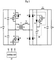
- Fig. 1 is a circuit diagram of a DC-DC converter circuit which is an embodiment of the present invention.
- Each of these switching elements S1 and S2 is a semiconductor switching element, and may, for example, be an IGBT (insulation gate type bipolar transistor) or a MOS-FET.
- a primary winding np of a transformer T is connected between the point of connection between the capacitors C1 and C2 and the point of connection between the switching elements S1 and S2.
- Respective free wheel diodes (clamp diodes) df1 and df2 are connected in reverse parallel to the switching elements S1 and S2. Moreover a control unit CT is provided, which outputs respective control signals G1 and G2 to control terminals of the switching elements S1 and S2 for alternatingly turning these switching elements S1 and S2 ON and OFF, on either side of inactive intervals.
- the primary side of this DC-DC converter is built as a half bridge type inverter circuit.
- the secondary side of this DC-DC converter has the following structure.
- a secondary diode circuit which includes secondary diodes D1 through D4 connected as a bridge for current adjustment is connected to a secondary winding ns of the transformer T, and a filter circuit which consists of a series circuit of a smoothing reactor L 0 and a smoothing capacitor C 0 is connected between the rectification outputs of these secondary diodes D1 through D4.
- This filter circuit could also consist only of the smoothing reactor L0.
- a regeneration snubber circuit SN is connected between the rectification outputs of the secondary diodes D1 through D4, and includes a series circuit of a discharge blocking diode Ds1 and a snubber capacitor Cs, and a switching element S3 for regeneration which is connected in parallel with said discharge blocking diode Ds.
- this regeneration snubber circuit SN is connected in parallel to a first secondary diode circuit which consists of the series circuit (via the secondary winding ns) of the secondary diodes D1 and D4, and to a second secondary diode circuit which consists of the series circuit (via the secondary winding ns) of the secondary diodes D2 and D3.
- the switching element S3 for regeneration may, for example, consist of a MOS-FET.
- a control signal G3 from the control unit CT is inputted to a control terminal of the switching element for regeneration S3.
- Fig. 2 is a time chart.
- the control signals G1 and G2 are not outputted, and due to this both the switching elements S1 and S2 are OFF.
- the reactor L 0 on the secondary side is the source of current, and half of the output current I 0 flows in each of the rectification diodes D1 through D4 (the free wheeling state) .
- ns (V) Vin ⁇ ns/np (numbers of windings) is generated in the secondary winding ns of the transformer T, and the current in the diodes D1 and D4 starts to increase.
- Vin is the input voltage to the primary winding np.
- the current in the diodes D1 and D4 becomes I 0 and the current in the diodes D2 and D3 becomes zero, and they go into the cutoff state and the current changeover terminates.
- the current in the diodes D1 and D4 increases, and the current in the diodes D2 and D3 progressively decreases to be less than zero.
- the fact that the current in the diodes D2 and D3 progressively decreases to be less than zero is because current flows in reverse from the cathodes to the anodes, so that a shunt current (through current) flows in all of the diodes D1 through D4; and, due thereto, energy is accumulated in the leakage inductance Le.
- the above described induced voltage is absorbed after t2 by the snubber capacitor Cs.
- the current in the diodes D2 and D3 becomes zero, and at t3 the current in the diodes D1 and D4 becomes I 0 .
- the control signal G3 goes to ON, and the switching element S3 for regeneration goes to ON .
- the switching element S1 Since before t4 the switching element S1 is ON, accordingly energy is accumulated in the leakage inductance Le by the output current I 0 ; but, when t4 arrives, this energy is emitted via the diodes D1 and D4. Due to this, the output current I 0 is divided between a current which flows through the diodes D1 and D4 on the basis of this emitted energy, and the discharge current from the snubber capacitor Cs.
- the output current I 0 is only the discharge current of the snubber capacitor Cs.
- the ON time period Tb of the control signal may be controlled to be a bit shorter. Due to this, it is possible to reduce the amount of discharge of the snubber capacitor Cs. When this is done, the amount of charging also decreases, since the voltage of the snubber capacitor Cs rises. If this is done, it is possible to reduce the currents flowing in the switching element S3, the secondary diodes D1 through D4, and the discharge element diode Ds1. Moreover, pulsation of the voltage of the snubber capacitor Cs is reduced.
- the voltage of the snubber capacitor Cs assumes a state in which its charging amount and its discharge amount are balanced. For example although, when the output current has been increased, the amount of discharge increases and the voltage of the snubber capacitor Cs tends to decrease, since the amount of charging increases due to this voltage decrease, accordingly the voltage of the snubber capacitor Cs is restored to its value which has been determined by the ON time period of the switching element S3. Thus, even if the load condition changes, the operation is such that the voltage of the snubber capacitor Cs becomes approximately constant.
- Fig. 3 is a circuit diagram of a DC-DC converter circuit which is another embodiment of the present invention.
- the first secondary diode D1 and the second secondary diode D2 for two phase half wave current adjustment are connected to the two output terminals respectively, while the load is connected between the output side of a reactor L 0 which is connected to the cathode side terminals of the secondary diodes D1 and D2, and the center tap of the transformer T.
- a first regeneration snubber circuit is connected between A-K of the secondary diode D1 (i.e.
- the first regeneration snubber circuit consists of a series circuit of a first discharge blocking diode Ds1-1 and a first snubber capacitor Cs-1, and a first switching element S3-1 for regeneration which is connected in parallel with the first discharge blocking diode Ds1-1.
- the second regeneration snubber circuit consists of a series circuit of a second discharge blocking diode Ds1-2 and a second snubber capacitor Cs-2, and a second switching element S3-2 for regeneration which is connected in parallel with the second discharge blocking diode Ds1-2.
- a control unit (not shown in the figures) turns the primary side switching elements S1 and S2 alternately ON and OFF within one cycle. And, in synchronization with turning the primary side switching element S1 OFF, this control unit turns the second regeneration switching element S3-2 to OFF for just a predetermined time interval Tb from this OFF timing. Moreover, in synchronization with turning the primary side switching element S2 OFF, the control unit turns the first regeneration switching element S3-1 to ON for just the predetermined time interval Tb from this OFF timing.
- the time interval Tb is set to the time period in which the charge which has been charged into the snubber capacitor Cs-2, and which originates in the reverse recovery time trr when the secondary diode D2 was turned OFF, discharges. Due to this, the charge which was accumulated in the snubber capacitor Cs-2 is all discharged in this time interval Tb.
- the time interval Tb is set to the time period in which the charge which has been charged into the snubber capacitor Cs-1, and which originates in the reverse recovery time trr when the secondary diode D1 was turned OFF, discharges. Due to this, the charge which was accumulated in the snubber capacitor Cs-1 is all discharged in this time interval Tb
- Fig. 4 is a circuit diagram of a DC-DC converter circuit which is yet another embodiment of the present invention.
- this DC-DC converter differs from the converter of Fig. 3 is that it is arranged for only one snubber capacitor to be used, and for it to be possible to use this snubber capacitor Cs in common in both the first regeneration snubber circuit and also the second regeneration snubber circuit.
- it is arranged for it to be possible to utilize the snubber capacitor Cs in common in both of the regeneration snubber circuits, by connecting together the anode of the first discharge blocking diode Ds1-1 of the first regeneration snubber circuit and the anode of the second discharge blocking diode Ds1-2 of the second regeneration snubber circuit, and by connecting the snubber capacitor Cs to this connection point.
- the operation of this converter is the same as the operation of the converter shown in Fig. 3 and described above.
- Fig. 5 is a circuit diagram of a DC-DC converter circuit which is still another embodiment of the present invention.
- this DC-DC converter differs from the converter of Fig. 4 is that it is arranged for only one switching element for regeneration to be used, and for it to be possible to use this switching element for regeneration in common in both the first regeneration snubber circuit and also the second regeneration snubber circuit.
- the anode of a first diode D5 for interference prevention is connected to the point of connection of the anode of the secondary diode D1 and the cathode of the first discharge blocking diode Ds1-1.
- the anode of a second diode D6 for interference prevention is connected to the point of connection of the anode of the secondary diode D2 and the cathode of the second discharge blocking diode Ds1-1 [sic].
- the cathode of the first diode D5 for interference prevention and the cathode of the second diode D6 for interference prevention are connected together, and the switching element S3 for regeneration is connected between this connection point and the snubber capacitor Cs.
- the operation of this converter is the same as the operation of the converter shown in Fig. 1 .
- the DC-DC converters of the various embodiments described above provide the following beneficial effects.
Landscapes
- Engineering & Computer Science (AREA)
- Power Engineering (AREA)
- Dc-Dc Converters (AREA)
Claims (7)
- Gleichstromwandler, umfassend:einen Schaltkreis mit einer Vielzahl primärseitiger Schaltelemente (S1, S2), die so angeordnet sind, dass sie mit einem inaktiven Intervall in der Schaltperiode, worin jeder der jeweiligen Schalter (S1, S2) AUS ist, abwechselnd EIN geschaltet werden,einen Transformator (T) mit einer primärseitigen Wicklung (np), wobei die Ausgabe des Schaltkreises an die primärseitige Wicklung angelegt wird, wobei der Transformator eine Ausgangsspannung, die mit einem vorbestimmten Spannungsänderungsverhältnis geändert wurde, an eine sekundärseitige Wicklung (ns) abgibt;eine sekundäre Diodenschaltung, die eine Vielzahl von Gleichrichterdioden (D1 bis D4) enthält, die mit der sekundärseitigen Wicklung (ns) des Transformators (T) verbunden sind und Ausgangsanschlüsse aufweisen;eine mit der sekundären Diodenschaltung parallel verbundene Lösch- bzw. Snubber-Schaltung (SN) für eine Regeneration, die eine Reihenschaltung einer Entladungs-Sperrdiode (Ds1) und eines Lösch- bzw. Snubber-Kondensators (Cs) und ein Schaltelement (S3) für eine Regeneration enthält, das mit der Entladungs-Sperrdiode (Ds1) parallel verbunden ist;eine Filterschaltung (Lo, Ro, Co), die zwischen Ausgangsanschlüsse der sekundären Diodenschaltung geschaltet ist;gekennzeichnet durcheine Steuerungseinheit (CT), die angeordnet ist, um das Schaltelement (S3) für eine Regeneration für eine vorbestimmte Zeitspanne (Tb) innerhalb des inaktiven Intervalls EIN zu schalten;wobei die vorbestimmte Zeitspanne (Tb) auf annähernd die Zeitspanne eingestellt wird, während der die im Snubber-Kondensator (Cs) akkumulierte Ladung sich entlädt.
- Gleichstromwandler nach Anspruch 1, wobei die Filterschaltung eine Glättungsspule (Lo) aufweist.
- Gleichstromwandler nach Anspruch 1, wobei die Filterschaltung eine Reihenschaltung einer Glättungsspule (Lo) und eines Glättungskondensators (Co) aufweist.
- Gleichstromwandler nach Anspruch 1, wobei die sekundäre Diodenschaltung eine Brücken-Gleichrichtungsschaltung aufweist, in der vier sekundäre Dioden (D1 bis D4) in Brückenschaltung verbunden sind.
- Gleichstromwandler nach Anspruch 1, wobei
die sekundärseitige Wicklung (ns) des Transformators (T) von einer Wicklung gebildet wird, in der zwei Ausgangsanschlüsse und eine Mittenabzweigung vorgesehen sind, die sekundäre Diodenschaltung von ersten und zweiten sekundären Dioden (D1, D2) gebildet wird, von denen jede mit einem der beiden Ausgangsanschlüsse der sekundärseitigen Wicklung (ns) verbunden ist, und die Snubber-Schaltung für eine Regeneration von ersten und zweiten Snubber-Schaltungen (Ds1-1, S3-1, Cs-1, Ds1-2, S3-2, Cs-2) für eine Regeneration gebildet wird, welche mit den ersten und zweiten sekundären Dioden (D1, D2) jeweils parallel verbunden sind;
die erste Snubber-Schaltung (Ds1-1, Cs-1, S3-1) für eine Regeneration eine Reihenschaltung einer ersten Entladungs-Sperrdiode (Ds1-1) und eines ersten Snubber-Kondensators (Cs-1) und ein erstes Schaltelement (S3-1) für eine Regeneration umfasst, das mit der ersten Entladungs-Sperrdiode (Ds1-1) parallel verbunden ist; und
die zweite Snubber-Schaltung (Dsl-2, Cs-2, S3-2) für eine Regeneration eine Reihenschaltung einer zweiten Entladungs-Sperrdiode (Dsl-2) und eines zweiten Snubber-Kondensators (Cs-2) und ein zweites Schaltelement (S3-2) für eine Regeneration umfasst, das mit der zweiten Entladungs-Sperrdiode (Ds1-2) parallel verbunden ist. - Gleichstromwandler nach Anspruch 5, wobei der erste Snubber-Kondensator (Cs-1) und der zweite Snubber-Kondensator (Cs-2) von einem einzigen Snubber-Kondensator (Cs) gebildet werden.
- Gleichstromwandler nach Anspruch 6, wobei das erste Schaltelement (S3-1) für eine Regeneration und das zweite Schaltelement (S3-2) für eine Regeneration von einem einzigen Schaltelement (S3) für eine Regeneration gebildet werden.
Applications Claiming Priority (2)
| Application Number | Priority Date | Filing Date | Title |
|---|---|---|---|
| JP2008072671 | 2008-12-12 | ||
| PCT/JP2009/053361 WO2010067629A1 (ja) | 2008-12-12 | 2009-02-25 | Dc-dcコンバータ回路 |
Publications (3)
| Publication Number | Publication Date |
|---|---|
| EP2372890A1 EP2372890A1 (de) | 2011-10-05 |
| EP2372890A4 EP2372890A4 (de) | 2017-05-10 |
| EP2372890B1 true EP2372890B1 (de) | 2019-10-16 |
Family
ID=42242621
Family Applications (1)
| Application Number | Title | Priority Date | Filing Date |
|---|---|---|---|
| EP09831735.7A Active EP2372890B1 (de) | 2008-12-12 | 2009-02-25 | Gleichstromwandler mit aktivem Entlastungkreis |
Country Status (5)
| Country | Link |
|---|---|
| US (1) | US8873259B2 (de) |
| EP (1) | EP2372890B1 (de) |
| KR (1) | KR101496941B1 (de) |
| CN (1) | CN101842971B (de) |
| WO (1) | WO2010067629A1 (de) |
Families Citing this family (28)
| Publication number | Priority date | Publication date | Assignee | Title |
|---|---|---|---|---|
| JP5168603B2 (ja) * | 2010-01-26 | 2013-03-21 | 株式会社デンソー | スイッチング装置 |
| JP5565186B2 (ja) * | 2010-08-09 | 2014-08-06 | 富士電機株式会社 | 電力変換装置 |
| US8547711B2 (en) * | 2010-11-19 | 2013-10-01 | General Electric Company | LLC converter active snubber circuit and method of operation thereof |
| JP5507017B2 (ja) * | 2011-11-21 | 2014-05-28 | 三菱電機株式会社 | Dc/dcコンバータ |
| CN105743332A (zh) * | 2011-12-21 | 2016-07-06 | 九尊城网络科技(深圳)有限公司 | 电源电路 |
| AT512409B1 (de) * | 2012-02-06 | 2013-08-15 | Fronius Int Gmbh | Ac/dc-spannungswandler und betriebsverfahren hierfür |
| JP5987496B2 (ja) * | 2012-06-27 | 2016-09-07 | 株式会社日立情報通信エンジニアリング | Dc−dcコンバータ |
| CN104854771B (zh) | 2012-10-29 | 2019-07-19 | 苹果公司 | 感应电力传输系统的接收器和用于控制该接收器的方法 |
| DE102012111828B4 (de) * | 2012-12-05 | 2016-09-29 | Universität Kassel | Konverter |
| JP5930978B2 (ja) * | 2013-01-15 | 2016-06-08 | 三菱電機株式会社 | Dc/dcコンバータ |
| JP6201586B2 (ja) * | 2013-09-30 | 2017-09-27 | 三菱電機株式会社 | Dc/dcコンバータ |
| KR20150049962A (ko) * | 2013-10-31 | 2015-05-08 | 삼성전기주식회사 | 전력 공급 장치 및 그 제어방법 |
| US20150188411A1 (en) * | 2013-12-27 | 2015-07-02 | O2Micro Inc | Dc/dc converters and output circuits thereof |
| CN105099196A (zh) * | 2014-05-16 | 2015-11-25 | 天宝电子(惠州)有限公司 | 一种电源变换器 |
| JP6402378B2 (ja) * | 2014-09-02 | 2018-10-10 | 京都電機器株式会社 | Dc−dcコンバータ装置 |
| US9680386B2 (en) * | 2014-09-23 | 2017-06-13 | Analog Devices Global | Minimum duty cycle control for active snubber |
| US9450491B2 (en) | 2014-10-23 | 2016-09-20 | Qualcomm Incorporated | Circuits and methods providing three-level signals at a synchronous buck converter |
| DE102015207607A1 (de) * | 2015-04-24 | 2016-10-27 | Schmidhauser Ag | Bidirektionaler Gleichspannungswandler |
| US10103638B1 (en) * | 2017-08-09 | 2018-10-16 | Infineon Technologies Austria Ag | Flyback converter with capacitor module and switching module |
| US11444553B2 (en) * | 2018-02-12 | 2022-09-13 | Ingeteam Power Technology, SA | Electrical power conversion system and associated method |
| EP3544163B1 (de) * | 2018-03-21 | 2020-09-16 | General Electric Technology GmbH | Wandler |
| CN108551163B (zh) * | 2018-06-22 | 2024-04-05 | 重庆金山科技(集团)有限公司 | 储能元件能量泄放与回收电路、高压电源、能量发生器及方法 |
| CN112119578B (zh) * | 2018-07-13 | 2024-02-06 | 赤多尼科两合股份有限公司 | 电力供应电路、控制方法和电设备 |
| JP7166843B2 (ja) * | 2018-08-28 | 2022-11-08 | キヤノン株式会社 | 電源装置及び画像形成装置 |
| US11349401B1 (en) * | 2021-01-25 | 2022-05-31 | Semiconductor Components Industries, Llc | Method and system of a power converter with secondary side active clamp |
| CN114785165B (zh) * | 2022-06-20 | 2022-11-08 | 广东首航智慧新能源科技有限公司 | 一种交流/直流变换器、电源模组及其故障检测方法 |
| CN115133788B (zh) * | 2022-07-01 | 2026-02-27 | 亚瑞源科技(深圳)有限公司 | 一种具有电压钳制之全桥相移转换器 |
| CN117639197B (zh) * | 2023-11-30 | 2024-06-04 | 中国建筑第四工程局有限公司 | 一种多路高压直流电源无缝切换电路及方法 |
Family Cites Families (16)
| Publication number | Priority date | Publication date | Assignee | Title |
|---|---|---|---|---|
| JP2754411B2 (ja) * | 1989-09-20 | 1998-05-20 | 富士電機株式会社 | 電力変換装置のスナバ回路 |
| JPH04236165A (ja) * | 1991-01-11 | 1992-08-25 | Fuji Electric Co Ltd | ロスレス・スイッチングスナバ回路 |
| US5173846A (en) * | 1991-03-13 | 1992-12-22 | Astec International Ltd. | Zero voltage switching power converter |
| JP2514872B2 (ja) * | 1991-06-12 | 1996-07-10 | 山洋電気株式会社 | 直流電源装置 |
| US5351179A (en) * | 1993-03-05 | 1994-09-27 | Digital Equipment Corporation | Lossless active snubber for half-bridge output rectifiers |
| JP3400443B2 (ja) * | 1999-06-22 | 2003-04-28 | ティーディーケイ株式会社 | スイッチング電源装置 |
| JP4773002B2 (ja) * | 2001-08-17 | 2011-09-14 | 株式会社三社電機製作所 | メッキ用電源装置 |
| JP2003189618A (ja) * | 2001-12-20 | 2003-07-04 | Matsushita Electric Ind Co Ltd | スイッチング電源装置 |
| DE60212463T2 (de) * | 2002-04-30 | 2007-02-01 | Det International Holding Ltd., George Town | Schaltnetzteil mit snubber-netzwerk |
| JP4326264B2 (ja) * | 2003-06-06 | 2009-09-02 | 新電元工業株式会社 | スイッチングコンバータ |
| JP2005027394A (ja) * | 2003-06-30 | 2005-01-27 | Eta Electric Industry Co Ltd | スイッチング電源装置 |
| US6980447B1 (en) * | 2004-10-18 | 2005-12-27 | Artesyn Technologies, Inc. | Active snubber circuit for synchronous rectifier |
| JP4561360B2 (ja) * | 2004-12-28 | 2010-10-13 | サンケン電気株式会社 | 直流変換装置 |
| US7161331B2 (en) * | 2005-04-11 | 2007-01-09 | Yuan Ze University | Boost converter utilizing bi-directional magnetic energy transfer of coupling inductor |
| DE102005030601A1 (de) * | 2005-06-30 | 2007-01-11 | Siemens Ag Österreich | Netzteil mit Vollbrückenschaltung und großem Regelungsbereich |
| JP2008079403A (ja) | 2006-09-20 | 2008-04-03 | Kawamura Electric Inc | 低損失コンバータ |
-
2009
- 2009-02-25 EP EP09831735.7A patent/EP2372890B1/de active Active
- 2009-02-25 WO PCT/JP2009/053361 patent/WO2010067629A1/ja not_active Ceased
- 2009-02-25 KR KR1020107005170A patent/KR101496941B1/ko active Active
- 2009-02-25 US US12/680,240 patent/US8873259B2/en active Active
- 2009-02-25 CN CN2009801008794A patent/CN101842971B/zh active Active
Non-Patent Citations (1)
| Title |
|---|
| None * |
Also Published As
| Publication number | Publication date |
|---|---|
| CN101842971A (zh) | 2010-09-22 |
| US8873259B2 (en) | 2014-10-28 |
| KR20110094162A (ko) | 2011-08-22 |
| KR101496941B1 (ko) | 2015-02-27 |
| US20110280048A1 (en) | 2011-11-17 |
| CN101842971B (zh) | 2013-04-24 |
| WO2010067629A1 (ja) | 2010-06-17 |
| EP2372890A4 (de) | 2017-05-10 |
| EP2372890A1 (de) | 2011-10-05 |
Similar Documents
| Publication | Publication Date | Title |
|---|---|---|
| EP2372890B1 (de) | Gleichstromwandler mit aktivem Entlastungkreis | |
| US6349044B1 (en) | Zero voltage zero current three level dc-dc converter | |
| US6525513B1 (en) | Soft switching topological circuit in boost or buck converter | |
| US9143044B2 (en) | Apparatus and method for pulse width modulation control for switching power converters | |
| JP4988925B2 (ja) | インバータ回路 | |
| US5982638A (en) | Single stage power converter with regenerative snubber and power factor correction | |
| US8184458B2 (en) | Power converter load line control | |
| US20020136033A1 (en) | Switching power supply | |
| EP3249795B1 (de) | Gleichstromwandler | |
| CN111478612B (zh) | 一种相位关联稳压管钳位的辅助谐振换流极逆变器 | |
| JP3402361B2 (ja) | スイッチング電源 | |
| US6487094B1 (en) | High efficiency DC-DC power converter | |
| KR101441602B1 (ko) | 인버터 회로 | |
| Wu et al. | Analysis and design for a new ZVS dc–dc converter with active clamping | |
| JP6129244B2 (ja) | Dc/dcコンバータ | |
| JP4914519B2 (ja) | Dc−dcコンバータ回路 | |
| KR101656021B1 (ko) | 직렬공진형 컨버터 | |
| KR101106505B1 (ko) | 소프트 스위칭 투-인덕터 부스트 컨버터 | |
| JP3069565B1 (ja) | スイッチング電源装置 | |
| Lin et al. | Implementation of a parallel zero-voltage switching forward converter with less power switches | |
| EP2385618B1 (de) | Gleichspannungswandlerschaltung | |
| JPH08103080A (ja) | 高入力力率電源回路およびこの電源回路の過電流保護回路 | |
| JP2003033029A (ja) | Dc−dcコンバータ | |
| JPH09252576A (ja) | 直流−直流変換装置のスナバ回路 | |
| JPH03139168A (ja) | 直列共振形コンバータ |
Legal Events
| Date | Code | Title | Description |
|---|---|---|---|
| PUAI | Public reference made under article 153(3) epc to a published international application that has entered the european phase |
Free format text: ORIGINAL CODE: 0009012 |
|
| 17P | Request for examination filed |
Effective date: 20110325 |
|
| AK | Designated contracting states |
Kind code of ref document: A1 Designated state(s): AT BE BG CH CY CZ DE DK EE ES FI FR GB GR HR HU IE IS IT LI LT LU LV MC MK MT NL NO PL PT RO SE SI SK TR |
|
| DAX | Request for extension of the european patent (deleted) | ||
| REG | Reference to a national code |
Ref country code: DE Ref legal event code: R079 Ref document number: 602009060184 Country of ref document: DE Free format text: PREVIOUS MAIN CLASS: H02M0003280000 Ipc: H02M0003335000 |
|
| RA4 | Supplementary search report drawn up and despatched (corrected) |
Effective date: 20170410 |
|
| RIC1 | Information provided on ipc code assigned before grant |
Ipc: H02M 3/335 20060101AFI20170404BHEP Ipc: H02M 1/34 20070101ALI20170404BHEP |
|
| STAA | Information on the status of an ep patent application or granted ep patent |
Free format text: STATUS: EXAMINATION IS IN PROGRESS |
|
| 17Q | First examination report despatched |
Effective date: 20181214 |
|
| GRAP | Despatch of communication of intention to grant a patent |
Free format text: ORIGINAL CODE: EPIDOSNIGR1 |
|
| STAA | Information on the status of an ep patent application or granted ep patent |
Free format text: STATUS: GRANT OF PATENT IS INTENDED |
|
| INTG | Intention to grant announced |
Effective date: 20190508 |
|
| GRAS | Grant fee paid |
Free format text: ORIGINAL CODE: EPIDOSNIGR3 |
|
| GRAA | (expected) grant |
Free format text: ORIGINAL CODE: 0009210 |
|
| STAA | Information on the status of an ep patent application or granted ep patent |
Free format text: STATUS: THE PATENT HAS BEEN GRANTED |
|
| AK | Designated contracting states |
Kind code of ref document: B1 Designated state(s): AT BE BG CH CY CZ DE DK EE ES FI FR GB GR HR HU IE IS IT LI LT LU LV MC MK MT NL NO PL PT RO SE SI SK TR |
|
| REG | Reference to a national code |
Ref country code: GB Ref legal event code: FG4D |
|
| REG | Reference to a national code |
Ref country code: CH Ref legal event code: EP |
|
| REG | Reference to a national code |
Ref country code: DE Ref legal event code: R096 Ref document number: 602009060184 Country of ref document: DE |
|
| REG | Reference to a national code |
Ref country code: IE Ref legal event code: FG4D |
|
| REG | Reference to a national code |
Ref country code: AT Ref legal event code: REF Ref document number: 1192267 Country of ref document: AT Kind code of ref document: T Effective date: 20191115 |
|
| REG | Reference to a national code |
Ref country code: NL Ref legal event code: FP |
|
| REG | Reference to a national code |
Ref country code: LT Ref legal event code: MG4D |
|
| REG | Reference to a national code |
Ref country code: AT Ref legal event code: MK05 Ref document number: 1192267 Country of ref document: AT Kind code of ref document: T Effective date: 20191016 |
|
| PG25 | Lapsed in a contracting state [announced via postgrant information from national office to epo] |
Ref country code: ES Free format text: LAPSE BECAUSE OF FAILURE TO SUBMIT A TRANSLATION OF THE DESCRIPTION OR TO PAY THE FEE WITHIN THE PRESCRIBED TIME-LIMIT Effective date: 20191016 Ref country code: PL Free format text: LAPSE BECAUSE OF FAILURE TO SUBMIT A TRANSLATION OF THE DESCRIPTION OR TO PAY THE FEE WITHIN THE PRESCRIBED TIME-LIMIT Effective date: 20191016 Ref country code: LT Free format text: LAPSE BECAUSE OF FAILURE TO SUBMIT A TRANSLATION OF THE DESCRIPTION OR TO PAY THE FEE WITHIN THE PRESCRIBED TIME-LIMIT Effective date: 20191016 Ref country code: NO Free format text: LAPSE BECAUSE OF FAILURE TO SUBMIT A TRANSLATION OF THE DESCRIPTION OR TO PAY THE FEE WITHIN THE PRESCRIBED TIME-LIMIT Effective date: 20200116 Ref country code: AT Free format text: LAPSE BECAUSE OF FAILURE TO SUBMIT A TRANSLATION OF THE DESCRIPTION OR TO PAY THE FEE WITHIN THE PRESCRIBED TIME-LIMIT Effective date: 20191016 Ref country code: GR Free format text: LAPSE BECAUSE OF FAILURE TO SUBMIT A TRANSLATION OF THE DESCRIPTION OR TO PAY THE FEE WITHIN THE PRESCRIBED TIME-LIMIT Effective date: 20200117 Ref country code: LV Free format text: LAPSE BECAUSE OF FAILURE TO SUBMIT A TRANSLATION OF THE DESCRIPTION OR TO PAY THE FEE WITHIN THE PRESCRIBED TIME-LIMIT Effective date: 20191016 Ref country code: FI Free format text: LAPSE BECAUSE OF FAILURE TO SUBMIT A TRANSLATION OF THE DESCRIPTION OR TO PAY THE FEE WITHIN THE PRESCRIBED TIME-LIMIT Effective date: 20191016 Ref country code: PT Free format text: LAPSE BECAUSE OF FAILURE TO SUBMIT A TRANSLATION OF THE DESCRIPTION OR TO PAY THE FEE WITHIN THE PRESCRIBED TIME-LIMIT Effective date: 20200217 Ref country code: BG Free format text: LAPSE BECAUSE OF FAILURE TO SUBMIT A TRANSLATION OF THE DESCRIPTION OR TO PAY THE FEE WITHIN THE PRESCRIBED TIME-LIMIT Effective date: 20200116 Ref country code: SE Free format text: LAPSE BECAUSE OF FAILURE TO SUBMIT A TRANSLATION OF THE DESCRIPTION OR TO PAY THE FEE WITHIN THE PRESCRIBED TIME-LIMIT Effective date: 20191016 |
|
| PG25 | Lapsed in a contracting state [announced via postgrant information from national office to epo] |
Ref country code: IS Free format text: LAPSE BECAUSE OF FAILURE TO SUBMIT A TRANSLATION OF THE DESCRIPTION OR TO PAY THE FEE WITHIN THE PRESCRIBED TIME-LIMIT Effective date: 20200224 Ref country code: HR Free format text: LAPSE BECAUSE OF FAILURE TO SUBMIT A TRANSLATION OF THE DESCRIPTION OR TO PAY THE FEE WITHIN THE PRESCRIBED TIME-LIMIT Effective date: 20191016 |
|
| REG | Reference to a national code |
Ref country code: DE Ref legal event code: R097 Ref document number: 602009060184 Country of ref document: DE |
|
| PG2D | Information on lapse in contracting state deleted |
Ref country code: IS |
|
| PG25 | Lapsed in a contracting state [announced via postgrant information from national office to epo] |
Ref country code: EE Free format text: LAPSE BECAUSE OF FAILURE TO SUBMIT A TRANSLATION OF THE DESCRIPTION OR TO PAY THE FEE WITHIN THE PRESCRIBED TIME-LIMIT Effective date: 20191016 Ref country code: DK Free format text: LAPSE BECAUSE OF FAILURE TO SUBMIT A TRANSLATION OF THE DESCRIPTION OR TO PAY THE FEE WITHIN THE PRESCRIBED TIME-LIMIT Effective date: 20191016 Ref country code: CZ Free format text: LAPSE BECAUSE OF FAILURE TO SUBMIT A TRANSLATION OF THE DESCRIPTION OR TO PAY THE FEE WITHIN THE PRESCRIBED TIME-LIMIT Effective date: 20191016 Ref country code: RO Free format text: LAPSE BECAUSE OF FAILURE TO SUBMIT A TRANSLATION OF THE DESCRIPTION OR TO PAY THE FEE WITHIN THE PRESCRIBED TIME-LIMIT Effective date: 20191016 Ref country code: IS Free format text: LAPSE BECAUSE OF FAILURE TO SUBMIT A TRANSLATION OF THE DESCRIPTION OR TO PAY THE FEE WITHIN THE PRESCRIBED TIME-LIMIT Effective date: 20200216 |
|
| PLBE | No opposition filed within time limit |
Free format text: ORIGINAL CODE: 0009261 |
|
| STAA | Information on the status of an ep patent application or granted ep patent |
Free format text: STATUS: NO OPPOSITION FILED WITHIN TIME LIMIT |
|
| PG25 | Lapsed in a contracting state [announced via postgrant information from national office to epo] |
Ref country code: SK Free format text: LAPSE BECAUSE OF FAILURE TO SUBMIT A TRANSLATION OF THE DESCRIPTION OR TO PAY THE FEE WITHIN THE PRESCRIBED TIME-LIMIT Effective date: 20191016 Ref country code: IT Free format text: LAPSE BECAUSE OF FAILURE TO SUBMIT A TRANSLATION OF THE DESCRIPTION OR TO PAY THE FEE WITHIN THE PRESCRIBED TIME-LIMIT Effective date: 20191016 |
|
| 26N | No opposition filed |
Effective date: 20200717 |
|
| REG | Reference to a national code |
Ref country code: CH Ref legal event code: PL |
|
| GBPC | Gb: european patent ceased through non-payment of renewal fee |
Effective date: 20200225 |
|
| REG | Reference to a national code |
Ref country code: BE Ref legal event code: MM Effective date: 20200229 |
|
| PG25 | Lapsed in a contracting state [announced via postgrant information from national office to epo] |
Ref country code: MC Free format text: LAPSE BECAUSE OF FAILURE TO SUBMIT A TRANSLATION OF THE DESCRIPTION OR TO PAY THE FEE WITHIN THE PRESCRIBED TIME-LIMIT Effective date: 20191016 Ref country code: LU Free format text: LAPSE BECAUSE OF NON-PAYMENT OF DUE FEES Effective date: 20200225 |
|
| PG25 | Lapsed in a contracting state [announced via postgrant information from national office to epo] |
Ref country code: CH Free format text: LAPSE BECAUSE OF NON-PAYMENT OF DUE FEES Effective date: 20200229 Ref country code: SI Free format text: LAPSE BECAUSE OF FAILURE TO SUBMIT A TRANSLATION OF THE DESCRIPTION OR TO PAY THE FEE WITHIN THE PRESCRIBED TIME-LIMIT Effective date: 20191016 Ref country code: LI Free format text: LAPSE BECAUSE OF NON-PAYMENT OF DUE FEES Effective date: 20200229 |
|
| PG25 | Lapsed in a contracting state [announced via postgrant information from national office to epo] |
Ref country code: GB Free format text: LAPSE BECAUSE OF NON-PAYMENT OF DUE FEES Effective date: 20200225 Ref country code: FR Free format text: LAPSE BECAUSE OF NON-PAYMENT OF DUE FEES Effective date: 20200229 Ref country code: IE Free format text: LAPSE BECAUSE OF NON-PAYMENT OF DUE FEES Effective date: 20200225 |
|
| PG25 | Lapsed in a contracting state [announced via postgrant information from national office to epo] |
Ref country code: BE Free format text: LAPSE BECAUSE OF NON-PAYMENT OF DUE FEES Effective date: 20200229 |
|
| PGFP | Annual fee paid to national office [announced via postgrant information from national office to epo] |
Ref country code: NL Payment date: 20210217 Year of fee payment: 13 |
|
| PGFP | Annual fee paid to national office [announced via postgrant information from national office to epo] |
Ref country code: DE Payment date: 20210217 Year of fee payment: 13 |
|
| PG25 | Lapsed in a contracting state [announced via postgrant information from national office to epo] |
Ref country code: TR Free format text: LAPSE BECAUSE OF FAILURE TO SUBMIT A TRANSLATION OF THE DESCRIPTION OR TO PAY THE FEE WITHIN THE PRESCRIBED TIME-LIMIT Effective date: 20191016 Ref country code: MT Free format text: LAPSE BECAUSE OF FAILURE TO SUBMIT A TRANSLATION OF THE DESCRIPTION OR TO PAY THE FEE WITHIN THE PRESCRIBED TIME-LIMIT Effective date: 20191016 Ref country code: CY Free format text: LAPSE BECAUSE OF FAILURE TO SUBMIT A TRANSLATION OF THE DESCRIPTION OR TO PAY THE FEE WITHIN THE PRESCRIBED TIME-LIMIT Effective date: 20191016 |
|
| PG25 | Lapsed in a contracting state [announced via postgrant information from national office to epo] |
Ref country code: MK Free format text: LAPSE BECAUSE OF FAILURE TO SUBMIT A TRANSLATION OF THE DESCRIPTION OR TO PAY THE FEE WITHIN THE PRESCRIBED TIME-LIMIT Effective date: 20191016 |
|
| REG | Reference to a national code |
Ref country code: DE Ref legal event code: R119 Ref document number: 602009060184 Country of ref document: DE |
|
| REG | Reference to a national code |
Ref country code: NL Ref legal event code: MM Effective date: 20220301 |
|
| PG25 | Lapsed in a contracting state [announced via postgrant information from national office to epo] |
Ref country code: NL Free format text: LAPSE BECAUSE OF NON-PAYMENT OF DUE FEES Effective date: 20220301 |
|
| PG25 | Lapsed in a contracting state [announced via postgrant information from national office to epo] |
Ref country code: DE Free format text: LAPSE BECAUSE OF NON-PAYMENT OF DUE FEES Effective date: 20220901 |