EP2374217B1 - Kreuzkopplungs-störungslöschung in mehreren empfangszweigen mit unabhängigen demodulationssignalen - Google Patents
Kreuzkopplungs-störungslöschung in mehreren empfangszweigen mit unabhängigen demodulationssignalen Download PDFInfo
- Publication number
- EP2374217B1 EP2374217B1 EP08875430.4A EP08875430A EP2374217B1 EP 2374217 B1 EP2374217 B1 EP 2374217B1 EP 08875430 A EP08875430 A EP 08875430A EP 2374217 B1 EP2374217 B1 EP 2374217B1
- Authority
- EP
- European Patent Office
- Prior art keywords
- signal
- receive
- frequency
- branch
- demodulation
- Prior art date
- Legal status (The legal status is an assumption and is not a legal conclusion. Google has not performed a legal analysis and makes no representation as to the accuracy of the status listed.)
- Active
Links
Images


Classifications
-
- H—ELECTRICITY
- H04—ELECTRIC COMMUNICATION TECHNIQUE
- H04B—TRANSMISSION
- H04B7/00—Radio transmission systems, i.e. using radiation field
- H04B7/002—Reducing depolarization effects
Definitions
- the present invention relates to techniques for cross-coupling interference cancellation in multiple receive branches with independent demodulation signals.
- cross-polarization interference i.e. due to signal portions of one polarization being coupled to the other polarization and vice versa.
- a signal may more generally also be referred to as a cross-coupled interference signal.
- the cross-polarization interference may be due to, e.g. non-ideal antennas or link-related fading phenomena.
- XPIC cross-polarization interference cancellation
- Differences in the carrier frequency can be avoided by using the same demodulation frequency in all receive branches, i.e. for both polarizations.
- a common oscillator may be used to supply the same demodulation signal to demodulators in the different receive branches.
- both receivers use the same demodulation frequency and undesirable differences in the carrier frequency between the cross coupling signal path and the compensation signal path are avoided.
- this concept requires extra cabling and synchronization hardware. This is undesirable in view of costs, especially for outdoor units.
- LANKL B ET AL "CROSS-POLARIZATION INTERFERENCE CANCELLATION IN THE PRESENCE OF DELAY EFFECTS", DIGITAL TECHNOLOGY - SPANNING THE UNIVERSE. PHILADELPHIA, JUNE 12 - 15, 1988; [INTERNATIONAL CONFERENCE ON COMMUNICATIONS], NEW YORK, IEEE, US, vol. VOL. 3 OF 3, no. 1988, 12 June 1988 (1988-06-12), pages 1355-1361 , discloses cross-coupling interference cancellation in multiple receive branches with independent demodulation signals.
- LANKL B ET AL "Fully digital ATDE's and XPIC's for a STM-1 cochannel radio system family", 19890611; 19890611 - 19890614, 11 June 1989 (1989-06-11), pages 1013-1019 , discloses a fully digital cross-coupling interference cancellation.
- a method of receiving data is provided.
- a first receive signal is received in a first receive branch.
- the first receive signal is demodulated on the basis of a first demodulation signal having a first demodulation frequency.
- a second receive signal is received in a second receive branch.
- the second receive signal is demodulated on the basis of a second demodulation signal having a second demodulation frequency.
- a compensation signal is extracted from the first receive signal.
- the method further includes generating a first digital value, which represents the first demodulation frequency in the second receive branch and generating a second digital value, which represents the second demodulation frequency in the second receive branch.
- the compensation signal is phase rotated on the basis of the first digital value and second digital value.
- the second receive signal is combined with the phase rotated first compensation signal.
- a receiver equipment includes a first receive branch for receiving a first receive signal.
- the first receive branch has a first demodulation oscillator configured to supply a first demodulation signal for demodulating the first receive signal.
- the first demodulation signal has a first demodulation frequency.
- the receiver equipment includes a second receive branch for receiving a second receive signal.
- the second receive branch has a second demodulation oscillator configured to supply a second demodulation signal for demodulating the second receive signal.
- the second demodulation signal has a second demodulation frequency.
- a compensation branch is provided for extracting a compensation signal from the first receive signal.
- a first frequency counter is provided in the first receive branch.
- the first frequency counter is configured to generate a first digital value, which represents the first demodulation frequency in the second receive branch.
- a second frequency counter is provided in the second receive branch.
- the second frequency counter is configured to generate a second digital value, which represents the second demodulation frequency in the second receive branch.
- the receiver equipment includes a phase rotating function receiving the first compensation signal to accomplish a phase rotation on the basis of the first digital value and second digital value.
- a combiner is provided for combining the second receive signal with the phase rotated first compensation signal.
- a first receive signal e.g. corresponding to a first signal polarization
- the first receive signal is demodulated on the basis of a first demodulation signal having a first demodulation frequency.
- a second receive signal e.g. corresponding to a second signal polarization orthogonal to the first signal polarization, is received in a second receive branch.
- the second receive signal is demodulated on the basis of a second demodulation signal having a second demodulation frequency.
- a first compensation signal is extracted from the first receive signal.
- a first digital value is generated, which represents the first demodulation frequency in the second receive branch.
- a second digital value is generated, which represents the second demodulation frequency in the second receive branch.
- a phase rotation of the first compensation signal is accomplished on the basis of the first digital value and the second digital value.
- the second receive signal is combined with the phase rotated first compensation signal.
- the first compensation signal and the first digital value may be transmitted on the same digital channel from the first receive branch to the second receive branch.
- the first demodulation signal For generating the first digital value, the first demodulation signal may be frequency divided, and for generating the second digital value, the second demodulation signal may be frequency divided.
- a second compensation signal may be extracted from the second receive signal.
- generating a third digital value may be generated, which represents the first demodulation frequency in the first receive branch
- a fourth digital value may be generated, which represents the second demodulation frequency in the first receive branch.
- the second compensation signal may then be phase rotated on the basis of the third digital value and fourth digital value, and the first receive signal may be combined with the phase rotated second compensation signal.
- the second compensation signal and the fourth digital value may be transmitted on the same digital channel from the second receive branch to the first receive branch.
- the first demodulation signal may be frequency divided, and for generating the fourth digital value, the second demodulation signal may be frequency divided.
- a symbol frequency of the second receive signal may transmitted to the first receive branch together with the second compensation signal, e.g. as a local clock signal and a local hold signal of the second receive branch.
- the first digital value may then be generated in the first receive branch as a ratio including the symbol frequency of the second receive signal, and the second digital value may be generated in the second receive branch as a ratio including to the symbol frequency of the second receive signal.
- a symbol frequency of the first receive signal may be transmitted to the second receive branch together with the first compensation signal, e.g. as a local clock signal and a local hold signal of the first receive branch.
- the third digital value may then be generated in the second receive branch as a ratio including the symbol frequency of the first receive signal, and the fourth digital value may be generated in the first receive branch as a ratio including the symbol frequency of the first receive signal.
- a communication system with cross-coupling interference cancellation and exchange of a digital compensation signal information concerning the frequency of the demodulation signal can be efficiently exchanged using the same digital interface as for the compensation signal. It is merely required to transmit additional data, which can be accomplished on the basis of a comparatively low clock rate. Transmitting the demodulation signal itself, e.g. for accomplishing a synchronization of the demodulation signals in the different receive branches can be avoided.
- each of the receive branches may correct any difference modulation between the cross-coupling interference signal path and the compensation path.
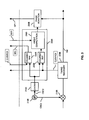
- Fig. 1 illustrates signal paths of cross-coupling interference signals and compensation signals in a communication system with multiple receive branches.
- a first transmit branch with a first transmit modulator 100A and a second transmit branch with a second transmit modulator 100B are provided.
- a first receive branch 200A with a first receive demodulator 210A, and second receive branch 200B with a second receive demodulator 210B are provided.
- the first transmit branch and the second transmit branch may correspond to separate hardware units and therefore be regarded as separate transmitters.
- the first receive branch 200A and the second receive branch 200B may correspond to separate hardware units and therefore be regarded as separate receivers.
- first transmit branch and the first receive branch 200A are provided for transferring signals with horizontal polarization
- second transmit branch and the second receive branch 200B are provided for transmitting signals with vertical polarization.
- other configurations of the different branches could be used as well.
- the different branches could correspond to different circular polarizations.
- a signal with horizontal polarization is transmitted.
- the signal is modulated on the basis of a first modulation oscillator signal having a first modulation frequency f TH .
- a signal with vertical polarization is transmitted.
- the signal is modulated on the basis of a second modulation oscillator signal having a second modulation frequency f TV .
- the first demodulator 210A demodulates the received signal on the basis of a first demodulation oscillator signal having a first demodulation frequency f RH .
- the second demodulator 210B demodulates the received signal on the basis of a second demodulation oscillator signal having a second demodulation frequency f RV .
- a frequency recovery unit 215A of the first receive branch 200A which accomplishes carrier recovery and synchronization, automatically finds, i.e. estimates, the difference between demodulation and modulation frequency, i.e. the difference (f RH - f TH ) between the first demodulation frequency f RH and the first modulation frequency f TH .
- This frequency difference is therefore known in the first receive branch 200A.
- a first digital receive signal 10A is provided at the output of the frequency recovery unit 215A.
- the first receive signal has a corresponding digital symbol timing, which includes a digital timing clock and a hold signal indicating valid data symbols (not illustrated).
- a frequency recovery unit 215B of the first receive branch 200B which accomplishes carrier recovery and synchronization, automatically finds, i.e. estimates, the difference between demodulation and modulation frequency, i.e. the difference (f RV - f TV ) between the second demodulation frequency f RV and the second modulation frequency f TV .
- This frequency difference is therefore known in the second receive branch 200B.
- a second digital receive signal 10B is provided at the output of the timing recovery unit 215B.
- the second digital receive signal 10B has a corresponding digital symbol timing, which includes a digital timing clock and a hold signal indicating valid data symbols (not illustrated).
- the receiver architecture of Fig. 1 includes a compensation branch with a first XPIC filter 270A and a first summing node 280A in the first receive branch 200A, and a further compensation branch with a second XPIC filter 270B and a second summing node 280B in the second receive branch 200B.
- a first digital compensation signal CP1 is extracted from the first digital receive signal 10A and combined with the second receive signal by the second XPIC filter 270B and the second summing node 280B.
- a second digital compensation signal CP2 is extracted from the second digital receive signal 10B and combined with the second receive signal by the first XPIC filter 270B and the first summing node 280B.
- a first compensation path thus extends from a diverging point 110A, located in the signal path between the first transmit branch and the first receive branch 200A, via the signal path of the first receive signal 10A and the first compensation signal CP1, to the summing node 280B in the second receive branch 200B.
- a second compensation path extends from a diverging point 110A, located in the signal path between the second transmit branch and the second receive branch 2008, via the signal path of the second receive signal 10B and the second compensation signal CP2, to the summing node 280A in the second receive branch 200A.
- a first cross-coupling path extends from the diverging point 110A, located in the signal path between the first transmit branch and the first receive branch 200A, via a merging point 115B, located in the signal path between the second transmit branch and the second receive branch 200B, to the summing node 280B in the second receive branch 200B.
- a second cross-coupling path extends from the diverging point 110B, located in the signal path between the second transmit branch and the second receive branch 200B, via a merging point 115A, located in the signal path between the first transmit branch and the first receive branch 200A, to the summing node 280A in the second receive branch 200A.
- the points 110A, 110B, 115A, and 115B merely serve to illustrate the cross-coupling paths and do not imply that the cross-coupling interference signals are actually transmitted between specific physical nodes.
- the first and second compensation paths cross an interface between the first receive branch 200A and the second receive branch 200B.
- the first compensation signal CP1 will be phase rotated by the known frequency difference (-f RH + f TH ), as illustrated at node 240A.
- the first compensation signal CP1 will be phase rotated by the known frequency difference (f RV - f TV ), as illustrated at node 260B.
- the second compensation signal CP2 will be phase rotated by the known frequency difference (-f RV + f TV ), as illustrated at node 240B.
- the first compensation signal CP2 After passing the interface the first compensation signal CP2 will be phase rotated by the known frequency difference (f RH - f TH ), as illustrated at node 260A. These phase rotations are due to the compensation signals CP1, CP2 being transmitted between different clock domains and cannot be avoided.
- a small difference between the accumulated phase rotations over the cross-coupling path and the accumulated phase rotations over the compensation path allows for an efficient cancellation of the cross-coupling interference signal.
- the quality of cross-coupling interference cancellation degrades.
- a small difference in the accumulated phase rotations may be achieved by including a phase-rotation correction into the compensation path.
- a phase rotation corresponding to the frequency difference (f RH -f RV ) may be included into the signal path of the first compensation signal CP1, as illustrated at node 250A.
- the frequency difference (f RH -f RV ) is evaluated at node 230A.
- first compensation path: -f RH +f RH -f TH -f RH +f TH -f RV +f RH +f RV -f TV -f TV
- a phase rotation corresponding to the frequency difference (-f RH +f RV ) may be included into the signal path of the second compensation signal CP2, as illustrated at node 250B.
- the frequency difference (-f RH +f RV ) is evaluated at node 230B.
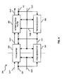
- Fig. 2 schematically illustrates a portion of a first receive branch in the receiver equipment
- Fig. 3 schematically illustrates a portion of a second receive branch in the receiver equipment.
- the first and second receive branches illustrated in Figs. 2 and 3 may be parts of the communication system as illustrated in Fig. 1 , i.e. Fig. 2 illustrates the first receive branch 200A and Fig. 3 illustrates the second receive branch 200B.
- Figs. 2 and 3 components which are similar to those of Fig. 1 have been designated with the same reference signs. Further explanations concerning these components can be obtained from the corresponding description with respect to Fig. 1 . Similarly, further details concerning the components illustrated in Fig. 1 may be taken from the corresponding description with respect to Figs. 2 and 3 .
- the compensation signals CP1, CP2 are exchanged as digital signals.
- the digital compensation signals CP1, CP2 are transferred between the different receive branches together with a corresponding clock signal and a corresponding hold signal.
- a first local clock signal CLKh of the first receive branch 200A and a first local hold signal HOh of the the first receive branch 200A are transmitted to the second receive branch 200B.
- a second local clock signal CLKv of the second receive branch 200B and a second local hold signal HOv of the second receive branch 200B are transmitted to the first receive branch 200A.
- both local clock signals CLKh, CLKv and both local hold signals HOh and HOv are available.
- the local clock signals CLKh, CLKv and the local hold signals HOh, HOv are generated by corresponding timing recovery units 220A, 220B.
- the local hold signals HOh, HOv indicate valid data symbols in corresponding data signals. That is to say, the first local hold signal HOh indicates valid data symbols in the first receive signal 10A and in the first compensation signal CP1, and the second local hold signal HOv indicates valid data symbols in the second receive signal 10B and in the second compensation signal CP2.
- the combination of the first local clock signal CLKh and the first local hold signal HOh is a representation of the symbol frequency of the corresponding data signals in the first receive branch 200A.
- the combination of the second local clock signal CLKv and the second local hold signal HOv is a representation of the symbol frequency of the corresponding data signals in the second receive branch 200B.
- the symbol frequency fSH of the data signals in the first receive branch 200A may be different from the symbol frequency fSV of the data signals in the second receive branch 200B.
- the concepts as explained in the following are also valid if the symbol frequencies fSH, fSV are identical.
- the first receive branch 200A includes the receive demodulator 210A, a first demodulation oscillator 212A, a first frequency divider 214A, and a first frequency evaluation block 230A (which corresponds to block 230A of Fig. 1 ).
- the frequency evaluation block 230A includes two frequency counters 232A, 234A and an angle computation unit 236A.
- the first receive branch 200A includes a first phase rotator 250A (which corresponds to node 250A of Fig. 1 ).
- the frequency counter 232A generates a digital value NHH on the basis of the first demodulation signal OSC1 and on the basis of the first symbol frequency fSH, i.e. on the basis of first local clock signal CLKh and the first local hold signal HOh.
- the frequency counter 234A generates a digital value NVH on the basis of the first demodulation signal OSC1 and on the basis of the first symbol frequency fSV.
- the first demodulation signal OSC1 as provided by the first demodulation oscillator 212A is supplied to the first receive demodulator 210A. Further, the first demodulation signal OSC1 is supplied to the first frequency divider 214A.
- the first frequency divider 214A divides the frequency of the first demodulation signal OSC1 by an appropriate factor, e.g. by a factor of about 1000 to shift the first demodulation frequency from a range of some GHz to a range of some MHz.
- the implementation of the frequency counters 232A, 234A is simplified. In the following, the frequency of the frequency divided first demodulation signal OSC1 will be designated by fOH.
- the second receive branch 200B includes the receive demodulator 210B, a second demodulation oscillator 214B, a second frequency divider 214B, and a second frequency evaluation block 230B (which corresponds to block 230B of Fig. 1 ).
- the frequency evaluation block 230B includes two frequency counters 232B, 234B and an angle computation unit 236B.
- the second receive branch 200B includes a second phase rotator 250B (which corresponds to node 250B of Fig. 1 ).
- the frequency counter 232B generates a digital value NVV on the basis of the second demodulation signal OSC2 and on the basis of the second symbol frequency fSV, i.e. on the basis of the second local clock signal CLKv and the second hold signal HOv.
- the frequency counter 234B generates a digital value NHV on the basis of the second demodulation signal OSC2 and on the basis of the second symbol frequency fSH.
- the second demodulation signal OSC2 as provided by the second demodulation oscillator 212B is supplied to the second receive demodulator 210B. Further, the second demodulation signal OSC2 is supplied to the second frequency divider 214B.
- the second frequency divider 214B divides the frequency of the second demodulation signal OSC2 by an appropriate factor. In the following, it will be assumed that this factor is the same as the frequency division factor of the first frequency divider 214A. As in the first receive branch 200A, shifting the frequency into a lower range simplifies the implementation of the frequency counters 232B, 234B. In the following, the frequency of the frequency divided second demodulation signal OSC2 will be designated by fOV.
- the digital values NVH and NHV are exchanged between the first and second receive branch 200A, 200B. This can be accomplished using the same digital transmission channels as for the compensation signal CP1, CP2. The additional bandwidth required to transmit the values NVH and NHV is negligible.
- the angle computation units 236A, 236B which may be implemented by hardware, software running on a control processor, or a combination of hardware and software , then compute a rotation phase angle on the basis of the digital values NHH, NVV, NVH, and NHV.
- Standard operations of digital signal processing may then be used to first obtain phase values ⁇ 1 , ⁇ 2 from the above frequency difference by incrementing a phase counter with a phase increment ⁇ 1 , ⁇ 2 .
- the trigonometric functions (Sinus and Cosinus) can be computed from the above phase values and be used in the phase rotators 250A, 250B for accomplishing a phase rotation of the compensation signals CP1, CP2.
- the two receive branches 200A, 200B may be different hardware units. Accordingly, the receive branches 200A, 200B may belong to different clock domains, e.g. different physical clock-nets having separate clock sources. Further, the symbol frequency fSH and fSV of the receive branches may be different. This has to be considered when exchanging digital data signals between the receive branches, i.e. the compensation signals CP1, CP2 and the digital values NHV, NVH.
- each receive branch 200A, 200B may be provided with a resampling device, which interpolates and samples one or more of the incoming data signals, i.e. the incoming compensation signal CP1 or CP2, and/or the incoming digital value NHV or NVH.
- the resampling device may be associated with nodes 260A, 260B of Fig. 1 .
- a separate resampling device may be provided for each incoming data signal.
- the signals CP1 and NHV may be combined in a single data signal
- the signals CP2 and NVH may be combine in a single data signal.
- the incoming data signal will be referred to DAT'
- the resampled incoming data signal will be referred to as DAT. It is to be understood that in the first receive branch 200A the incoming data signal DAT' may include the digital value NHV and/or the compensation signal CP1, and that in the second receive branch 200B the incoming data signal DAT' may include the digital value NVH and/or the compensation signal CP2.
- the resampling device 300 may be used in the receive branches 200A, 200B of Figs. 1-3 .
- the resampling device 300 is based on an asynchronous sampling concept, which allows for an efficient hardware implementation. In other implementations, synchronous sampling concepts may be used.
- the physical clock frequency is slightly higher than necessary, and not every clock edge indicates a new valid data symbol.
- the sequence of valid data symbols in the data stream is indicated by a hold signal, i.e. the local hold signal HOh as provided by the timing recovery unit 220A, or the local hold signal HOv provided by the timing recovery unit 220B.
- the resampling device 300 comprises a FIFO ("First In/First Out") buffer 320, a hold generator 340, an interpolation filter 360, and a timing recovery unit 380.
- FIFO First In/First Out
- the resampling device 300 has an external port with three signals CLK', HO', DAT' and an internal port with three signals CLK, HO, DAT.
- data is supplied via the incoming data signal DAT'.
- the data is accompanied by an external clock signal CLK' and, due to the asynchronous nature of the data, by an external hold signal HO'.
- the external clock signal CLK' and the external hold signal HO' will be formed by the local clock signal CLKh, CLKv and the local hold signal HOh, HOv of the other receive branch 200A, 200B. That is to say, if the resampling device 300 is located in the first receive branch 200A, the external clock signal CLK' will be the local clock signal CLKv of the second receive branch 200B, and the external hold signal HO' will be the local hold signal HOv of the second receive branch 200B.
- the external clock signal CLK' will be the local clock signal CLKh of the first receive branch 200A
- the external hold signal HO' will be the local hold signal HOh of the first receive branch 200A.
- the data is output by as the resampled incoming data signal DAT. Further, a local clock signal CLK and a local hold signal HO are supplied as input signals to the resampling device 300 at the internal port. If the resampling device 300 is located in the first receive branch 200A, the local clock signal CLK will be the local clock signal CLKh of the first receive branch 200A, and the local hold signal HO will be the local hold signal HOh of the first receive branch 200A.
- the local clock signal CLK will be the local clock signal CLKv of the second receive branch 200B
- the local hold signal HO will be the local hold signal HOv of the second receive branch 200B.
- the local clock signal CLK and the local hold signal CH can be considered as reference signals to which the incoming data signal DAT' is synchronized.
- the FIFO buffer 320 receives a data symbol at a clock edge of the external clock signal CLK', if the external hold signal HO' indicates a valid data symbol.
- the FIFO buffer 320 outputs a data symbol at a clock edge of the local clock signal CLK, if a further hold signal HOi indicates that a data symbol is to be retrieved.
- This further hold signal HOi is generated by the hold generator 340 and is also referred to as an intermediate hold signal.
- the hold generator 340 is configured to assure that, on average, the hold signals HO', HOi, indicate the same amount of valid data symbols, irrespective of the different clock signals CLK', CLK used for operating the input and output of the FIFO buffer 320.
- the valid data symbols of the incoming data signal DAT' are regenerated on the basis of the local clock signal. Otherwise, the incoming data signal DAT' is not changed.
- the interpolation filter 360 computes intermediate values from the incoming data signal DAT' as supplied from the FIFO buffer 320.
- the intermediate values are computed on the basis of a timing phase signal TAB provided by the timing recovery unit 380.
- the intermediate values are output from the interpolation filter 360 in the resampled incoming data signal DAT. This is accomplished on the basis of the local hold signal HO and the local clock signal CLK, i.e. a data symbol in the resampled incoming data signal DAT is output on a clock edge of the local clock signal CLK if the local hold signal HO indicates a valid data symbol.
- the rates of valid data symbols at the input and at the output of the interpolation filter 360 are different and are given by the intermediate hold signal HOi (at the input) and the local hold signal HO (at the output).
- the intermediate hold signal HOi and the local hold signal HO are supplied as input signals to the timing recovery unit 380.
- the timing recovery unit 380 receives the local clock signal CLK.
- the timing recovery unit 380 generates the timing phase signal TAB for the interpolation filter 320 on the basis of the intermediate hold signal HOi, the local hold signal HO, and the local clock signal CLK.
- Fig. 5 is a functional diagram schematically illustrating the hold generator 340.
- the hold generator 340 may include a first modulo counter implemented by a summing node 342 and a data register 344, a second modulo counter implemented by a summing node 356 and a data register 358, a gray-level encoder (GEC) 346, a gray-level decoder (GDC) 350, a further data register 352, and a comparator 354.
- GEC gray-level encoder
- GDC gray-level decoder
- a vertical dashed line schematically illustrates a border between different clock domains. Components shown on the left side of the vertical dashed line belong to a clock domain of the external clock signal CLK', and components shown on the right side of the vertical dashed line belong to a clock domain of the local clock signal CLK.
- the summing node 342 receives the external hold signal HO' at a first input.
- the first modulo counter counts the amount of valid data symbols indicated by the external hold signal HO'.
- the output of the first modulo counter is supplied to the clock domain of the local clock signal CLK using a gray-level encoding/gray-level decoding (GEC/GDC) interface, provided by the gray-level encoder 346, which is located in the clock domain of the external clock signal CLK', followed by the gray-level decoder 350, which is located in the clock domain of the local clock signal CLK.
- GOC/GDC gray-level encoding/gray-level decoding
- the output of the first modulo counter is received in the clock domain of the local clock signal CLK via the GEC/GDC interface and is supplied to the data register 352, which is operated on the basis of the local clock signal CLK.
- the output signal of the data register 352 is supplied to a first input of the comparator 354.
- An output signal of the second modulo counter is supplied to a second input of the comparator 354.
- the comparator 354 On the basis of a comparison between the signal supplied to its first input and the signal supplied to its second input, the comparator 354 generates the intermediate hold signal HOi.
- the summing node 356 receives the intermediate hold signal HOi at a first input.
- the data register 358 which is operated on the basis of the local clock signal CLK, receives the output signal of the summing node 356, and a feedback signal is supplied from the output of the data register 358 to a second input of the summing node 356.
- the second modulo counter counts the amount of valid data symbols indicated by the intermediate hold signal HOi.
- the intermediate hold signal HOi is generated on the basis of a comparison between the output signal of the first modulo counter, i.e. the amount of valid data symbols indicated by the external hold signal HO', and the output signal of the second modulo counter, i.e. the amount of valid data symbols indicated by the intermediate hold signal HOi.
- the comparator 354 generates the intermediate hold signal HOi in such a way that, on average, the number of valid data symbols indicated by the intermediate hold signal HOi is the same as the number of valid data symbols indicated by the external hold signal HO'. For example, if the first modulo counter outputs a larger value than the second modulo counter, the comparator 354 will generate the intermediate hold signal HOi with a hold value, i.e. a value indicating a valid data symbol. This may be referred to as "pushing" a hold value. Otherwise the intermediate hold signal will be generated without a hold value, which may be referred to as "dropping" a hold value.
- Fig. 6 is a functional diagram schematically illustrating the timing recovery unit 380.
- the timing recovery unit 380 comprises an up/down counter 362, a loop filter 364, and a number controlled oscillator (NCO) 366.
- NCO number controlled oscillator
- the local hold signal HO is supplied to a positive first input of the up/down counter 362, and the intermediate hold signal HOi is supplied to a negative second input of the up/down counter 362. Since the local hold signal HO and the intermediate hold signal HOi belong to the same clock domain, i.e. to the clock domain of the local clock signal CLK, they can be compared directly in the up/down counter 362. According to the hold signals HO, HOi, the up/down counter will be incremented or decrernented. That is to say, the up/down counter 362 will be incremented by the local hold signal indicating a valid data symbol, and the up/down counter 362 will be decrernented by the intermediate hold signal HOi indicating a valid data symbol. An output signal of the up/down counter 362 thus corresponds to a rate difference between the local hold signal HO and the intermediate hold signal HOi.
- the output signal of the up/down counter is supplied to the loop filter 364, which has a filter function F(s).
- the filtered output signal of the loop filter 364 is supplied to the number-controlled oscillator 366.
- the number-controlled oscillator 366 produces the timing phase signal TAB, and an overflow signal OFL which is supplied back to the up/down counter 362 as a feedback signal, thereby forming a closed control loop.
- the timing phase signal TAB delivered by the number-controlled oscillator 366 is a sequence of timing phases with a constant phase increment from sample to sample.
- the timing phase signal TAB is used as an input signal of the interpolation filter 360 ( Fig. 4 ).
- the timing phases indicate time positions at which the interpolated value is to be computed by the interpolation filter 360.
- the overflow signal OFL is generated at each zero-phase crossing of the timing phase signal TAB and is supplied to a third input for the up/down counter 362.
- the sign of the overflow signal OFL i.e. whether it is used to increment or to decrement the up/down counter, depends on the direction of the zero-phase crossing.
- the overflow signal OFL eventually indicates the difference of the rates of the two input hold signals HO, HOi.
- the output of the up/down counter 362 vanishes and the output of the loop filter 364, which is the input of the number-controlled oscillator 366, becomes constant.
- the resampling device 300 as explained in connection with Figs. 3-6 allows for efficiently transferring the digital data signals between different clock domains having different digital symbol timings.
- phase rotation correction can be implemented in a digital circuit, e.g. an ASIC ("Application Specific Integrated Circuit"), which can be shared by other digital signal processing functions. Exchanging the digital values can be digitally multiplexed together with the exchange of the compensation signals, which is allows for reusing existing functions.
- ASIC Application Specific Integrated Circuit
Landscapes
- Engineering & Computer Science (AREA)
- Computer Networks & Wireless Communication (AREA)
- Signal Processing (AREA)
- Digital Transmission Methods That Use Modulated Carrier Waves (AREA)
Claims (15)
- Verfahren zum Empfangen von Daten, umfassend:Empfangen eines ersten Empfangssignals (10A) in einem ersten Empfangszweig (200A), wobei das erste Empfangssignal (10A) auf der Basis eines ersten Demodulationssignals (OSC1) mit einer ersten Demodulationsfrequenz (fRH) demoduliert wird;Empfangen eines zweiten Empfangssignals (10B) in einem zweiten Empfangszweig (200B), wobei das zweite Empfangssignal (10B) auf der Basis eines zweiten Demodulationssignals (OSC2) mit einer zweiten Demodulationsfrequenz (fRV) demoduliert wird;Extrahieren eines ersten Kompensationssignals (CP1) aus dem ersten Empfangssignal (10A);Erzeugen eines ersten Digitalwerts (NVH), welcher die erste Demodulationsfrequenz (fRH) im zweiten Empfangszweig (200B) darstellt;Erzeugen eines zweiten Digitalwerts (NVV), welcher die zweite Demodulationsfrequenz (fRV) im zweiten Empfangszweig (200B) darstellt;Rotieren der Phase des ersten Kompensationssignals (CP1) auf der Basis des ersten Digitalwerts (NVH) und des zweiten Digitalwerts (NVV); undVerknüpfen des zweiten Empfangssignals (10B) mit dem phasenrotierten ersten Kompensationssignal (CP1).
- Verfahren nach Anspruch 1, umfassend:Übertragen des ersten Kompensationssignals (CP1) auf einem ersten Digitalkanal vom ersten Empfangszweig (200A) an den zweiten Empfangszweig (200B); undÜbertragen des ersten Digitalwerts (NVH) auf dem ersten Digitalkanal vom ersten Empfangszweig (200A) an den zweiten Empfangszweig (200B).
- Verfahren nach Anspruch 1 oder 2,
wobei das Erzeugen des ersten Digitalwerts (NVH) ein Teilen der Frequenz des ersten Demodulationssignals (OSC1) umfasst; und
wobei das Erzeugen des zweiten Digitalwerts (NVV) ein Teilen der Frequenz des zweiten Demodulationssignals (OSC2) umfasst. - Verfahren nach einem der vorhergehenden Ansprüche, umfassend:Extrahieren eines zweiten Kompensationssignals (CP2) aus dem zweiten Empfangssignal (10B);Erzeugen eines dritten Digitalwerts (NHH), welcher die erste Demodulationsfrequenz (fRH) im ersten Empfangszweig (100A) darstellt;Erzeugen eines vierten Digitalwerts (NHV), welcher die zweite Demodulationsfrequenz (fRV) im ersten Empfangszweig (100A) darstellt;Rotieren der Phase des zweiten Kompensationssignals (CP2) auf der Basis des dritten Digitalwerts (NHH) und des vierten Digitalwerts (NHV); undVerknüpfen des ersten Empfangssignals (10A) mit dem phasenrotierten zweiten Kompensationssignal (CP2).
- Verfahren nach Anspruch 4, umfassend:Übertragen des zweiten Kompensationssignals (CP2) auf einem zweiten Digitalkanal vom zweiten Empfangszweig (200B) an den ersten Empfangszweig (200A); undÜbertragen des vierten Digitalwerts (NHV) auf dem zweiten Digitalkanal vom zweiten Empfangszweig (200B) an den ersten Empfangszweig (200A).
- Verfahren nach Anspruch 5,
wobei das Erzeugen des dritten Digitalwerts (NHH) ein Teilen der Frequenz des ersten Demodulationssignals (OSC1) umfasst; und
wobei das Erzeugen des vierten Digitalwerts (NHV) ein Teilen der Frequenz des zweiten Demodulationssignals (OSC2) umfasst. - Verfahren nach einem der Ansprüche 4 bis 6,
wobei eine Symbolfrequenz (fSV) des zweiten Empfangssignals (10B) zusammen mit dem zweiten Kompensationssignal (CP2) an den ersten Empfangszweig (200A) übertragen wird;
wobei der erste Digitalwert (NVH) im ersten Empfangszweig (200A) in Bezug auf die Symbolfrequenz (fSV) des zweiten Empfangssignals (10B) erzeugt wird; und
wobei der zweite Digitalwert (NVV) im zweiten Empfangszweig (200B) in Bezug auf die Symbolfrequenz (fSV) des zweiten Empfangssignals (10B) erzeugt wird. - Verfahren nach einem der Ansprüche 4 bis 7,
wobei eine Symbolfrequenz (fSH) des ersten Empfangssignals (10A) zusammen mit dem ersten Kompensationssignal (CP1) an den zweiten Empfangszweig (200B) übertragen wird;
wobei der dritte Digitalwert (NHH) im ersten Empfangszweig (200A) in Bezug auf die Symbolfrequenz (fSH) des zweiten Empfangssignals (10B) erzeugt wird;
und
wobei der vierte Digitalwert (NHV) im ersten Empfangszweig (200A) in Bezug auf die Symbolfrequenz (fSH) des ersten Empfangssignals (10A) erzeugt wird. - Verfahren nach einem der vorhergehenden Ansprüche,
wobei der erste Empfangszweig (200A) das erste Empfangssignal (10A) auf der Basis einer ersten Signalpolarisation empfängt, und der zweite Empfangszweig (200B) das zweite Empfangssignal (10B) auf der Basis einer zweiten Signalpolarisation empfängt. - Empfängereinrichtung, umfassend:einen ersten Empfangszweig (200A) zum Empfangen eines ersten Empfangssignals (10A), wobei der erste Empfangszweig (200A) einen ersten Demodulationsoszillator (212A) aufweist, der so konfiguriert ist, dass er ein erstes Demodulationssignal (OSC1) zum Demodulieren des ersten Empfangssignals (10A) liefert, wobei das erste Demodulationssignal (OSC1) eine erste Demodulationsfrequenz (fRH) aufweist;einen zweiten Empfangszweig (200B) zum Empfangen eines zweiten Empfangssignals (10B), wobei der zweite Empfangszweig (200B) einen zweiten Demodulationsoszillator (212B) aufweist, der so konfiguriert ist, dass er ein zweites Demodulationssignal (OSC2) zum Demodulieren des zweiten Empfangssignals (10B) liefert, wobei das zweite Demodulationssignal (OSC2) eine zweite Demodulationsfrequenz (fRV) aufweist;einen ersten Kompensationszweig zum Extrahieren eines ersten Kompensationssignals (CP1) aus dem ersten Empfangssignal (10A);einen ersten Frequenzzähler (232A) im ersten Empfangszweig (200A), wobei der erste Frequenzzähler (232A) so konfiguriert ist, dass er einen ersten Digitalwert (NVH) erzeugt, welcher die erste Demodulationsfrequenz (fRH) im zweiten Empfangszweig (200B) darstellt;einen zweiten Frequenzzähler (232B) im zweiten Empfangszweig (200B), wobei der zweite Frequenzzähler (232B) so konfiguriert ist, dass er einen zweiten Digitalwert (NVV) erzeugt, welcher die zweite Demodulationsfrequenz (fRV) im zweiten Empfangszweig (200B) darstellt;eine erste Phasenrotationsfunktion (250A), die das erste Kompensationssignal (CP1) empfängt, um eine Phasenrotation auf der Basis des ersten Digitalwerts (NVH) und des zweiten Digitalwerts (NVV) zu erreichen; undeinen ersten Verknüpfer (270B, 280B) zum Verknüpfen des zweiten Empfangssignals (10B) mit dem phasenrotierten ersten Kompensationssignal (CP1).
- Empfängereinrichtung nach Anspruch 10, umfassend:einen ersten Digitalkanal, der so konfiguriert ist, dass er das erste Kompensationssignal (CP1) und den ersten Digitalwert (NVH) vom ersten Empfangszweig (200A) an den zweiten Empfangszweig (200B) überträgt.
- Empfängereinrichtung nach Anspruch 10 oder 11, umfassend:einen zweiten Kompensationszweig zum Extrahieren eines zweiten Kompensationssignals (CP2) aus dem zweiten Empfangssignal (10B);einen dritten Frequenzzähler (234A) im ersten Empfangszweig (200A), wobei der dritte Frequenzzähler (234A) so konfiguriert ist, dass er einen dritten Digitalwert (NHH) erzeugt, welcher die erste Demodulationsfrequenz (fRH) im ersten Empfangszweig (200A) darstellt;einen vierten Frequenzzähler (234B) im zweiten Empfangszweig (200B), wobei der vierte Frequenzzähler (234B) so konfiguriert ist, dass er einen vierten Digitalwert (NHV) erzeugt, welcher die zweite Demodulationsfrequenz (fRV) im ersten Empfangszweig (200A) darstellt;eine zweite Phasenrotationsfunktion (250B), die das zweite Kompensationssignal (CP2) empfängt, um eine Phasenrotation auf der Basis des dritten Digitalwerts (NHH) und des vierten Digitalwerts (NHV) zu erreichen; undeinen zweiten Verknüpfer (270A, 280A) zum Verknüpfen des ersten Empfangssignals (10A) mit dem phasenrotierten zweiten Kompensationssignal (CP2).
- Empfängereinrichtung nach Anspruch 12, umfassend:einen zweiten Digitalkanal, der so konfiguriert ist, dass er das zweite Kompensationssignal (CP2) und den vierten Digitalwert (NHV) vom zweiten Empfangszweig (200B) an den ersten Empfangszweig (200A) überträgt.
- Empfängereinrichtung nach einem der Ansprüche 10 bis 13, umfassend:einen ersten Frequenzteiler (214A) zum Teilen der Frequenz des ersten Demodulationssignals (OSC1); undeinen zweiten Frequenzteiler (214B) zum Teilen der Frequenz des zweiten Demodulationssignals (OSC2).
- Empfängereinrichtung nach einem der Ansprüche 10 bis 14,
wobei die Empfängereinrichtung so konfiguriert ist, dass sie das Verfahren nach einem der Ansprüche 1 bis 9 ausführt.
Applications Claiming Priority (1)
| Application Number | Priority Date | Filing Date | Title |
|---|---|---|---|
| PCT/EP2008/067134 WO2010066288A1 (en) | 2008-12-09 | 2008-12-09 | Cross-coupling interference cancellation in multiple receive branches with independent demodulation signals |
Publications (2)
| Publication Number | Publication Date |
|---|---|
| EP2374217A1 EP2374217A1 (de) | 2011-10-12 |
| EP2374217B1 true EP2374217B1 (de) | 2013-04-10 |
Family
ID=40940649
Family Applications (1)
| Application Number | Title | Priority Date | Filing Date |
|---|---|---|---|
| EP08875430.4A Active EP2374217B1 (de) | 2008-12-09 | 2008-12-09 | Kreuzkopplungs-störungslöschung in mehreren empfangszweigen mit unabhängigen demodulationssignalen |
Country Status (2)
| Country | Link |
|---|---|
| EP (1) | EP2374217B1 (de) |
| WO (1) | WO2010066288A1 (de) |
Cited By (11)
| Publication number | Priority date | Publication date | Assignee | Title |
|---|---|---|---|---|
| WO2017187339A1 (en) * | 2016-04-25 | 2017-11-02 | Uhnder, Inc. | Vehicular radar system with self-interference cancellation |
| US9945943B2 (en) | 2016-04-07 | 2018-04-17 | Uhnder, Inc. | Adaptive transmission and interference cancellation for MIMO radar |
| US9971020B1 (en) | 2017-02-10 | 2018-05-15 | Uhnder, Inc. | Radar data buffering |
| US9989627B2 (en) | 2016-04-25 | 2018-06-05 | Uhnder, Inc. | Vehicular radar system with self-interference cancellation |
| US9989638B2 (en) | 2016-04-25 | 2018-06-05 | Uhnder, Inc. | Adaptive filtering for FMCW interference mitigation in PMCW radar systems |
| US10142133B2 (en) | 2016-04-25 | 2018-11-27 | Uhnder, Inc. | Successive signal interference mitigation |
| US10145954B2 (en) | 2016-04-07 | 2018-12-04 | Uhnder, Inc. | Software defined automotive radar systems |
| US10197671B2 (en) | 2016-09-16 | 2019-02-05 | Uhnder, Inc. | Virtual radar configuration for 2D array |
| US10261179B2 (en) | 2016-04-07 | 2019-04-16 | Uhnder, Inc. | Software defined automotive radar |
| US10324165B2 (en) | 2016-04-25 | 2019-06-18 | Uhnder, Inc. | PMCW—PMCW interference mitigation |
| US11846696B2 (en) | 2017-02-10 | 2023-12-19 | Uhnder, Inc. | Reduced complexity FFT-based correlation for automotive radar |
Families Citing this family (10)
| Publication number | Priority date | Publication date | Assignee | Title |
|---|---|---|---|---|
| US10573959B2 (en) | 2016-04-25 | 2020-02-25 | Uhnder, Inc. | Vehicle radar system using shaped antenna patterns |
| EP3449272B1 (de) | 2016-04-25 | 2022-11-02 | Uhnder, Inc. | Fahrzeugradarsystem mit einem gemeinsamen radar und kommunikationssystem, und verfahren zur verwaltung eines solchen systems in einem fahrzeug |
| US9753121B1 (en) | 2016-06-20 | 2017-09-05 | Uhnder, Inc. | Power control for improved near-far performance of radar systems |
| US11454697B2 (en) | 2017-02-10 | 2022-09-27 | Uhnder, Inc. | Increasing performance of a receive pipeline of a radar with memory optimization |
| US11105890B2 (en) | 2017-12-14 | 2021-08-31 | Uhnder, Inc. | Frequency modulated signal cancellation in variable power mode for radar applications |
| US12386029B2 (en) | 2018-01-29 | 2025-08-12 | Robert Bosch Gmbh | Millimeter wave automotive radar systems |
| US11474225B2 (en) | 2018-11-09 | 2022-10-18 | Uhnder, Inc. | Pulse digital mimo radar system |
| WO2020183392A1 (en) | 2019-03-12 | 2020-09-17 | Uhnder, Inc. | Method and apparatus for mitigation of low frequency noise in radar systems |
| WO2021144711A2 (en) | 2020-01-13 | 2021-07-22 | Uhnder, Inc. | Method and system for intefrence management for digital radars |
| US12498452B2 (en) | 2021-12-02 | 2025-12-16 | Robert Bosch Gmbh | Radar system with enhanced processing for increased contrast ratio, improved angular separability and accuracy, and elimination of ghost targets in a single-snapshot |
Family Cites Families (1)
| Publication number | Priority date | Publication date | Assignee | Title |
|---|---|---|---|---|
| DE602005021613D1 (de) * | 2005-03-31 | 2010-07-15 | Nokia Siemens Networks Spa | Kreuzpolarisationsübertragungssystem mit asynchronem Empfänger |
-
2008
- 2008-12-09 WO PCT/EP2008/067134 patent/WO2010066288A1/en not_active Ceased
- 2008-12-09 EP EP08875430.4A patent/EP2374217B1/de active Active
Cited By (14)
| Publication number | Priority date | Publication date | Assignee | Title |
|---|---|---|---|---|
| US10261179B2 (en) | 2016-04-07 | 2019-04-16 | Uhnder, Inc. | Software defined automotive radar |
| US9945943B2 (en) | 2016-04-07 | 2018-04-17 | Uhnder, Inc. | Adaptive transmission and interference cancellation for MIMO radar |
| US10145954B2 (en) | 2016-04-07 | 2018-12-04 | Uhnder, Inc. | Software defined automotive radar systems |
| US10215853B2 (en) | 2016-04-07 | 2019-02-26 | Uhnder, Inc. | Adaptive transmission and interference cancellation for MIMO radar |
| US9945935B2 (en) | 2016-04-25 | 2018-04-17 | Uhnder, Inc. | Digital frequency modulated continuous wave radar using handcrafted constant envelope modulation |
| US10324165B2 (en) | 2016-04-25 | 2019-06-18 | Uhnder, Inc. | PMCW—PMCW interference mitigation |
| US9989627B2 (en) | 2016-04-25 | 2018-06-05 | Uhnder, Inc. | Vehicular radar system with self-interference cancellation |
| US9989638B2 (en) | 2016-04-25 | 2018-06-05 | Uhnder, Inc. | Adaptive filtering for FMCW interference mitigation in PMCW radar systems |
| US10142133B2 (en) | 2016-04-25 | 2018-11-27 | Uhnder, Inc. | Successive signal interference mitigation |
| US10191142B2 (en) | 2016-04-25 | 2019-01-29 | Uhnder, Inc. | Digital frequency modulated continuous wave radar using handcrafted constant envelope modulation |
| WO2017187339A1 (en) * | 2016-04-25 | 2017-11-02 | Uhnder, Inc. | Vehicular radar system with self-interference cancellation |
| US10197671B2 (en) | 2016-09-16 | 2019-02-05 | Uhnder, Inc. | Virtual radar configuration for 2D array |
| US9971020B1 (en) | 2017-02-10 | 2018-05-15 | Uhnder, Inc. | Radar data buffering |
| US11846696B2 (en) | 2017-02-10 | 2023-12-19 | Uhnder, Inc. | Reduced complexity FFT-based correlation for automotive radar |
Also Published As
| Publication number | Publication date |
|---|---|
| EP2374217A1 (de) | 2011-10-12 |
| WO2010066288A1 (en) | 2010-06-17 |
Similar Documents
| Publication | Publication Date | Title |
|---|---|---|
| EP2374217B1 (de) | Kreuzkopplungs-störungslöschung in mehreren empfangszweigen mit unabhängigen demodulationssignalen | |
| US8244142B2 (en) | Optical receiver having fractional sampling | |
| Meyers et al. | Joint carrier phase and symbol timing recovery for PAM systems | |
| US9467246B2 (en) | Clock recovery method and clock recovery arrangement for coherent polarization multiplex receivers | |
| CN101652970B (zh) | 正交极化干扰补偿设备、解调器、接收站、及补偿正交极化干扰的方法 | |
| JP5601205B2 (ja) | 光受信器および光通信システム | |
| EP0587975A2 (de) | Diversity Funkempfänger | |
| US9473236B2 (en) | Relay apparatus, relay satellite, and satellite communication system | |
| JP3566788B2 (ja) | 交差偏波間補償装置 | |
| AU7643298A (en) | Method and apparatus for fine frequency synchronization in multi-carrier demodulation systems | |
| JP2004172975A (ja) | 両偏波受信装置及びそのローカル位相雑音低減方法 | |
| CN1369148A (zh) | 用于两个正交极化信号的接收机 | |
| CN101057470B (zh) | 使用多个源的载波恢复方法和装置 | |
| EP1363411A1 (de) | Verfahren und Vorrichtung zur Diversität | |
| WO2010041236A1 (en) | Estimating interference in multi channel systems | |
| EP0763919B1 (de) | QPSK-Demodulator mit Frequenz- und Phasennachlauf | |
| JP2000165339A (ja) | 送信lo同期方式を用いた両偏波伝送システム | |
| JP4285845B2 (ja) | 受信装置 | |
| US20220158750A1 (en) | Out-of-band communication channel for point-to-multi-point communications | |
| US5592507A (en) | Intermediate relay station of a digital microwave communication system using service channel for monitoring and controlling space and/or time diversity, heterodyne relay, phase control, frequency control, with phase shift keying modulation | |
| JP7540298B2 (ja) | デジタル受信装置 | |
| EP2015468A1 (de) | Basisbandkombinator für digitale Funkverbindungen | |
| US7974332B2 (en) | High-frequency HomePNA | |
| US7164733B1 (en) | Method and device for compensating for digital data demodulation phase uncertainty | |
| EP2374216B1 (de) | Kompensationstechniken für empfangssignale in verschiedenen taktdomänen |
Legal Events
| Date | Code | Title | Description |
|---|---|---|---|
| PUAI | Public reference made under article 153(3) epc to a published international application that has entered the european phase |
Free format text: ORIGINAL CODE: 0009012 |
|
| 17P | Request for examination filed |
Effective date: 20110707 |
|
| AK | Designated contracting states |
Kind code of ref document: A1 Designated state(s): AT BE BG CH CY CZ DE DK EE ES FI FR GB GR HR HU IE IS IT LI LT LU LV MC MT NL NO PL PT RO SE SI SK TR |
|
| DAX | Request for extension of the european patent (deleted) | ||
| GRAP | Despatch of communication of intention to grant a patent |
Free format text: ORIGINAL CODE: EPIDOSNIGR1 |
|
| GRAS | Grant fee paid |
Free format text: ORIGINAL CODE: EPIDOSNIGR3 |
|
| GRAP | Despatch of communication of intention to grant a patent |
Free format text: ORIGINAL CODE: EPIDOSNIGR1 |
|
| GRAA | (expected) grant |
Free format text: ORIGINAL CODE: 0009210 |
|
| AK | Designated contracting states |
Kind code of ref document: B1 Designated state(s): AT BE BG CH CY CZ DE DK EE ES FI FR GB GR HR HU IE IS IT LI LT LU LV MC MT NL NO PL PT RO SE SI SK TR |
|
| REG | Reference to a national code |
Ref country code: GB Ref legal event code: FG4D |
|
| REG | Reference to a national code |
Ref country code: CH Ref legal event code: EP Ref country code: AT Ref legal event code: REF Ref document number: 606491 Country of ref document: AT Kind code of ref document: T Effective date: 20130415 |
|
| REG | Reference to a national code |
Ref country code: IE Ref legal event code: FG4D |
|
| REG | Reference to a national code |
Ref country code: DE Ref legal event code: R096 Ref document number: 602008023808 Country of ref document: DE Effective date: 20130606 |
|
| PG25 | Lapsed in a contracting state [announced via postgrant information from national office to epo] |
Ref country code: SI Free format text: LAPSE BECAUSE OF FAILURE TO SUBMIT A TRANSLATION OF THE DESCRIPTION OR TO PAY THE FEE WITHIN THE PRESCRIBED TIME-LIMIT Effective date: 20130410 |
|
| REG | Reference to a national code |
Ref country code: AT Ref legal event code: MK05 Ref document number: 606491 Country of ref document: AT Kind code of ref document: T Effective date: 20130410 |
|
| REG | Reference to a national code |
Ref country code: NL Ref legal event code: VDEP Effective date: 20130410 Ref country code: LT Ref legal event code: MG4D |
|
| PG25 | Lapsed in a contracting state [announced via postgrant information from national office to epo] |
Ref country code: LT Free format text: LAPSE BECAUSE OF FAILURE TO SUBMIT A TRANSLATION OF THE DESCRIPTION OR TO PAY THE FEE WITHIN THE PRESCRIBED TIME-LIMIT Effective date: 20130410 Ref country code: IS Free format text: LAPSE BECAUSE OF FAILURE TO SUBMIT A TRANSLATION OF THE DESCRIPTION OR TO PAY THE FEE WITHIN THE PRESCRIBED TIME-LIMIT Effective date: 20130810 Ref country code: GR Free format text: LAPSE BECAUSE OF FAILURE TO SUBMIT A TRANSLATION OF THE DESCRIPTION OR TO PAY THE FEE WITHIN THE PRESCRIBED TIME-LIMIT Effective date: 20130711 Ref country code: ES Free format text: LAPSE BECAUSE OF FAILURE TO SUBMIT A TRANSLATION OF THE DESCRIPTION OR TO PAY THE FEE WITHIN THE PRESCRIBED TIME-LIMIT Effective date: 20130721 Ref country code: SE Free format text: LAPSE BECAUSE OF FAILURE TO SUBMIT A TRANSLATION OF THE DESCRIPTION OR TO PAY THE FEE WITHIN THE PRESCRIBED TIME-LIMIT Effective date: 20130410 Ref country code: NL Free format text: LAPSE BECAUSE OF FAILURE TO SUBMIT A TRANSLATION OF THE DESCRIPTION OR TO PAY THE FEE WITHIN THE PRESCRIBED TIME-LIMIT Effective date: 20130410 Ref country code: NO Free format text: LAPSE BECAUSE OF FAILURE TO SUBMIT A TRANSLATION OF THE DESCRIPTION OR TO PAY THE FEE WITHIN THE PRESCRIBED TIME-LIMIT Effective date: 20130710 Ref country code: BE Free format text: LAPSE BECAUSE OF FAILURE TO SUBMIT A TRANSLATION OF THE DESCRIPTION OR TO PAY THE FEE WITHIN THE PRESCRIBED TIME-LIMIT Effective date: 20130410 Ref country code: AT Free format text: LAPSE BECAUSE OF FAILURE TO SUBMIT A TRANSLATION OF THE DESCRIPTION OR TO PAY THE FEE WITHIN THE PRESCRIBED TIME-LIMIT Effective date: 20130410 Ref country code: FI Free format text: LAPSE BECAUSE OF FAILURE TO SUBMIT A TRANSLATION OF THE DESCRIPTION OR TO PAY THE FEE WITHIN THE PRESCRIBED TIME-LIMIT Effective date: 20130410 Ref country code: PT Free format text: LAPSE BECAUSE OF FAILURE TO SUBMIT A TRANSLATION OF THE DESCRIPTION OR TO PAY THE FEE WITHIN THE PRESCRIBED TIME-LIMIT Effective date: 20130812 |
|
| PG25 | Lapsed in a contracting state [announced via postgrant information from national office to epo] |
Ref country code: BG Free format text: LAPSE BECAUSE OF FAILURE TO SUBMIT A TRANSLATION OF THE DESCRIPTION OR TO PAY THE FEE WITHIN THE PRESCRIBED TIME-LIMIT Effective date: 20130710 Ref country code: PL Free format text: LAPSE BECAUSE OF FAILURE TO SUBMIT A TRANSLATION OF THE DESCRIPTION OR TO PAY THE FEE WITHIN THE PRESCRIBED TIME-LIMIT Effective date: 20130410 Ref country code: HR Free format text: LAPSE BECAUSE OF FAILURE TO SUBMIT A TRANSLATION OF THE DESCRIPTION OR TO PAY THE FEE WITHIN THE PRESCRIBED TIME-LIMIT Effective date: 20130410 Ref country code: CY Free format text: LAPSE BECAUSE OF FAILURE TO SUBMIT A TRANSLATION OF THE DESCRIPTION OR TO PAY THE FEE WITHIN THE PRESCRIBED TIME-LIMIT Effective date: 20130410 Ref country code: LV Free format text: LAPSE BECAUSE OF FAILURE TO SUBMIT A TRANSLATION OF THE DESCRIPTION OR TO PAY THE FEE WITHIN THE PRESCRIBED TIME-LIMIT Effective date: 20130410 |
|
| PG25 | Lapsed in a contracting state [announced via postgrant information from national office to epo] |
Ref country code: SK Free format text: LAPSE BECAUSE OF FAILURE TO SUBMIT A TRANSLATION OF THE DESCRIPTION OR TO PAY THE FEE WITHIN THE PRESCRIBED TIME-LIMIT Effective date: 20130410 Ref country code: CZ Free format text: LAPSE BECAUSE OF FAILURE TO SUBMIT A TRANSLATION OF THE DESCRIPTION OR TO PAY THE FEE WITHIN THE PRESCRIBED TIME-LIMIT Effective date: 20130410 Ref country code: EE Free format text: LAPSE BECAUSE OF FAILURE TO SUBMIT A TRANSLATION OF THE DESCRIPTION OR TO PAY THE FEE WITHIN THE PRESCRIBED TIME-LIMIT Effective date: 20130410 Ref country code: DK Free format text: LAPSE BECAUSE OF FAILURE TO SUBMIT A TRANSLATION OF THE DESCRIPTION OR TO PAY THE FEE WITHIN THE PRESCRIBED TIME-LIMIT Effective date: 20130410 |
|
| PLBE | No opposition filed within time limit |
Free format text: ORIGINAL CODE: 0009261 |
|
| STAA | Information on the status of an ep patent application or granted ep patent |
Free format text: STATUS: NO OPPOSITION FILED WITHIN TIME LIMIT |
|
| PG25 | Lapsed in a contracting state [announced via postgrant information from national office to epo] |
Ref country code: IT Free format text: LAPSE BECAUSE OF FAILURE TO SUBMIT A TRANSLATION OF THE DESCRIPTION OR TO PAY THE FEE WITHIN THE PRESCRIBED TIME-LIMIT Effective date: 20130410 Ref country code: RO Free format text: LAPSE BECAUSE OF FAILURE TO SUBMIT A TRANSLATION OF THE DESCRIPTION OR TO PAY THE FEE WITHIN THE PRESCRIBED TIME-LIMIT Effective date: 20130410 |
|
| 26N | No opposition filed |
Effective date: 20140113 |
|
| REG | Reference to a national code |
Ref country code: DE Ref legal event code: R097 Ref document number: 602008023808 Country of ref document: DE Effective date: 20140113 |
|
| REG | Reference to a national code |
Ref country code: CH Ref legal event code: PL |
|
| PG25 | Lapsed in a contracting state [announced via postgrant information from national office to epo] |
Ref country code: LU Free format text: LAPSE BECAUSE OF FAILURE TO SUBMIT A TRANSLATION OF THE DESCRIPTION OR TO PAY THE FEE WITHIN THE PRESCRIBED TIME-LIMIT Effective date: 20131209 |
|
| REG | Reference to a national code |
Ref country code: IE Ref legal event code: MM4A |
|
| REG | Reference to a national code |
Ref country code: FR Ref legal event code: ST Effective date: 20140829 |
|
| PG25 | Lapsed in a contracting state [announced via postgrant information from national office to epo] |
Ref country code: IE Free format text: LAPSE BECAUSE OF NON-PAYMENT OF DUE FEES Effective date: 20131209 Ref country code: LI Free format text: LAPSE BECAUSE OF NON-PAYMENT OF DUE FEES Effective date: 20131231 Ref country code: CH Free format text: LAPSE BECAUSE OF NON-PAYMENT OF DUE FEES Effective date: 20131231 |
|
| PG25 | Lapsed in a contracting state [announced via postgrant information from national office to epo] |
Ref country code: FR Free format text: LAPSE BECAUSE OF NON-PAYMENT OF DUE FEES Effective date: 20131231 |
|
| PG25 | Lapsed in a contracting state [announced via postgrant information from national office to epo] |
Ref country code: MC Free format text: LAPSE BECAUSE OF FAILURE TO SUBMIT A TRANSLATION OF THE DESCRIPTION OR TO PAY THE FEE WITHIN THE PRESCRIBED TIME-LIMIT Effective date: 20130410 |
|
| PG25 | Lapsed in a contracting state [announced via postgrant information from national office to epo] |
Ref country code: TR Free format text: LAPSE BECAUSE OF FAILURE TO SUBMIT A TRANSLATION OF THE DESCRIPTION OR TO PAY THE FEE WITHIN THE PRESCRIBED TIME-LIMIT Effective date: 20130410 |
|
| PG25 | Lapsed in a contracting state [announced via postgrant information from national office to epo] |
Ref country code: HU Free format text: LAPSE BECAUSE OF FAILURE TO SUBMIT A TRANSLATION OF THE DESCRIPTION OR TO PAY THE FEE WITHIN THE PRESCRIBED TIME-LIMIT; INVALID AB INITIO Effective date: 20081209 |
|
| PG25 | Lapsed in a contracting state [announced via postgrant information from national office to epo] |
Ref country code: MT Free format text: LAPSE BECAUSE OF FAILURE TO SUBMIT A TRANSLATION OF THE DESCRIPTION OR TO PAY THE FEE WITHIN THE PRESCRIBED TIME-LIMIT Effective date: 20130410 |
|
| PGFP | Annual fee paid to national office [announced via postgrant information from national office to epo] |
Ref country code: DE Payment date: 20231229 Year of fee payment: 16 |
|
| REG | Reference to a national code |
Ref country code: DE Ref legal event code: R119 Ref document number: 602008023808 Country of ref document: DE |
|
| PG25 | Lapsed in a contracting state [announced via postgrant information from national office to epo] |
Ref country code: DE Free format text: LAPSE BECAUSE OF NON-PAYMENT OF DUE FEES Effective date: 20250701 |
|
| PGFP | Annual fee paid to national office [announced via postgrant information from national office to epo] |
Ref country code: GB Payment date: 20251229 Year of fee payment: 18 |