EP2375449A2 - Dispositif d'imagerie à l'état solide - Google Patents
Dispositif d'imagerie à l'état solide Download PDFInfo
- Publication number
- EP2375449A2 EP2375449A2 EP20110161104 EP11161104A EP2375449A2 EP 2375449 A2 EP2375449 A2 EP 2375449A2 EP 20110161104 EP20110161104 EP 20110161104 EP 11161104 A EP11161104 A EP 11161104A EP 2375449 A2 EP2375449 A2 EP 2375449A2
- Authority
- EP
- European Patent Office
- Prior art keywords
- light
- optical waveguide
- imaging device
- solid
- state imaging
- Prior art date
- Legal status (The legal status is an assumption and is not a legal conclusion. Google has not performed a legal analysis and makes no representation as to the accuracy of the status listed.)
- Granted
Links
Images




Classifications
-
- H—ELECTRICITY
- H10—SEMICONDUCTOR DEVICES; ELECTRIC SOLID-STATE DEVICES NOT OTHERWISE PROVIDED FOR
- H10F—INORGANIC SEMICONDUCTOR DEVICES SENSITIVE TO INFRARED RADIATION, LIGHT, ELECTROMAGNETIC RADIATION OF SHORTER WAVELENGTH OR CORPUSCULAR RADIATION
- H10F39/00—Integrated devices, or assemblies of multiple devices, comprising at least one element covered by group H10F30/00, e.g. radiation detectors comprising photodiode arrays
- H10F39/80—Constructional details of image sensors
- H10F39/806—Optical elements or arrangements associated with the image sensors
- H10F39/8067—Reflectors
-
- G—PHYSICS
- G02—OPTICS
- G02B—OPTICAL ELEMENTS, SYSTEMS OR APPARATUS
- G02B7/00—Mountings, adjusting means, or light-tight connections, for optical elements
- G02B7/28—Systems for automatic generation of focusing signals
-
- H—ELECTRICITY
- H10—SEMICONDUCTOR DEVICES; ELECTRIC SOLID-STATE DEVICES NOT OTHERWISE PROVIDED FOR
- H10F—INORGANIC SEMICONDUCTOR DEVICES SENSITIVE TO INFRARED RADIATION, LIGHT, ELECTROMAGNETIC RADIATION OF SHORTER WAVELENGTH OR CORPUSCULAR RADIATION
- H10F39/00—Integrated devices, or assemblies of multiple devices, comprising at least one element covered by group H10F30/00, e.g. radiation detectors comprising photodiode arrays
- H10F39/80—Constructional details of image sensors
- H10F39/806—Optical elements or arrangements associated with the image sensors
-
- H—ELECTRICITY
- H10—SEMICONDUCTOR DEVICES; ELECTRIC SOLID-STATE DEVICES NOT OTHERWISE PROVIDED FOR
- H10F—INORGANIC SEMICONDUCTOR DEVICES SENSITIVE TO INFRARED RADIATION, LIGHT, ELECTROMAGNETIC RADIATION OF SHORTER WAVELENGTH OR CORPUSCULAR RADIATION
- H10F39/00—Integrated devices, or assemblies of multiple devices, comprising at least one element covered by group H10F30/00, e.g. radiation detectors comprising photodiode arrays
- H10F39/80—Constructional details of image sensors
- H10F39/805—Coatings
- H10F39/8057—Optical shielding
Definitions
- the present invention relates to a solid-state imaging device, and more particularly, to a solid-state imaging device for use in a digital still camera, a digital video camera, and the like.
- Japanese Patent No. 3592147 proposes a solid-state imaging device in which a part of pixels of an imaging device have a ranging function and the detection is made by a phase difference system.
- the phase difference system is a method in which optical images which pass through different regions on a pupil of a camera lens are compared and triangulation using a stereo image is used to detect the distance.
- a ranging pixel has between a microlens and a photoelectric conversion unit an opening which is off center with respect to an optical center of the microlens.
- the F value of the microlens for introducing light to the photoelectric conversion unit becomes larger, and the pixel size and the size of a diffraction image become almost the same.
- the present invention has been made in view of the above-mentioned problem, and an object of the present invention is to provide a solid-state imaging device which can carry out ranging with high precision, and in particular, which can carry out ranging with high precision even when the pixel size is small.
- a solid-state imaging device including a pixel includes: a photoelectric conversion unit for converting light into an electrical signal; an optical waveguide provided on an light incident side of the photoelectric conversion unit, the optical waveguide being configured so that light entering from a first direction is converted into a first waveguide mode and is guided and light entering from a second direction, which is different from the first direction, is converted into a second waveguide mode and is guided; and a light blocking member provided in the optical waveguide, for reducing more light in the second waveguide mode which is guided to the photoelectric conversion unit than light in the first waveguide mode which is guided to the photoelectric conversion unit.
- a solid-state imaging device which can carry out ranging with high precision, and in particular, which can carry out ranging with high precision even when the pixel size is small.
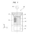
- FIG. 1 is a schematic sectional view illustrating a ranging pixel disposed in a part of a solid-state imaging device according to Embodiment 1.
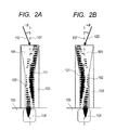
- FIG. 2A illustrates a waveguide mode when there is no light blocking member in an optical waveguide according to Embodiment 1.
- FIG. 2B illustrates another waveguide mode when there is no light blocking member in the optical waveguide according to Embodiment 1.
- FIG. 3A illustrates a waveguide mode in the optical waveguide when a light blocking member is disposed in the optical waveguide according to Embodiment 1.
- FIG. 3B illustrates another waveguide mode in the optical waveguide when the light blocking member is disposed in the optical waveguide according to Embodiment 1.
- FIG. 4 is a graph illustrating dependence of detected light intensity on incident angle in the pixel according to Embodiment 1.
- FIG. 5A is an explanatory view of a method of measuring the distance to a subject using the imaging device according to Embodiment 1.
- FIG. 5B is another explanatory view of the method of measuring the distance to the subject using the imaging device according to Embodiment 1.
- FIG. 5C is yet another explanatory view of the method of measuring the distance to the subject using the imaging device according to Embodiment 1.
- FIG. 6 illustrates an exemplary structure formed using a microlens on an light incident side of the optical waveguide according to Embodiment 1.
- FIG. 7A is an explanatory view of a manufacturing process step of the solid-state imaging device including the pixel according to Embodiment 1.
- FIG. 7B is an explanatory view of a manufacturing process step of the solid-state imaging device including the pixel according to Embodiment 1.
- FIG. 7C is an explanatory view of a manufacturing process step of the solid-state imaging device including the pixel according to Embodiment 1.
- FIG. 7D is an explanatory view of a manufacturing process step of the solid-state imaging device including the pixel according to Embodiment 1.
- FIG. 7E is an explanatory view of a manufacturing process step of the solid-state imaging device including the pixel according to Embodiment 1.
- FIG. 8 is a schematic sectional view illustrating a ranging pixel disposed in a part of a solid-state imaging device according to Embodiment 2.
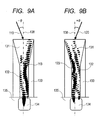
- FIG. 9A illustrates a waveguide mode when there is no light blocking member in an optical waveguide according to Embodiment 2.
- FIG. 9B illustrates another waveguide mode when there is no light blocking member in the optical waveguide according to Embodiment 2.
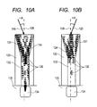
- FIG. 10A illustrates a waveguide mode in the optical waveguide when a light blocking member is disposed in the optical waveguide according to Embodiment 2.
- FIG. 10B illustrates another waveguide mode in the optical waveguide when the light blocking member is disposed in the optical waveguide according to Embodiment 2.
- FIG. 11 is a graph illustrating dependence of detected light intensity on incident angle in a pixel according to Embodiment 2.
- FIG. 12A illustrates an example in which a wiring member is formed in a clad member according to Embodiment 2.
- FIG. 12B illustrates an example in which a microlens is provided on an light incident side of the optical waveguide according to Embodiment 2.
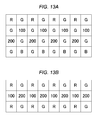
- FIG. 13A illustrates an exemplary arrangement of the ranging pixels in the imaging device according to Embodiment 1.
- FIG. 13B illustrates another exemplary arrangement of the ranging pixels in the imaging device according to Embodiment 1.
- the present invention uses the property that a light propagation state (waveguide mode) in a waveguide varies according to an incident angle of light flux which enters the waveguide.
- a following solid-state imaging device is materialized.
- a light blocking member is disposed in the waveguide, which enables detection of light which enters at a predetermined angle among the whole incident light, and thus, ranging may be carried out with high precision.
- Embodiment 1 an exemplary structure of a solid-state imaging device according to the present invention is described with reference to FIG. 1 .
- a pixel 100 has a ranging function and is disposed in a part of the solid-state imaging device of this embodiment.
- the pixel 100 includes from an light incident side (+z side) an light incident member 101, an optical waveguide (a core member 102 and a clad member 103) having therein a light blocking member 106, and a substrate 105 having therein a photoelectric conversion unit 104.
- the light blocking member 106 is disposed so as to be asymmetrical with respect to an yz plane including a central axis 107 of the optical waveguide.
- the central axis 107 of the optical waveguide is a central axis of the core member 102.
- the light incident member 101, the core member 102, and the clad member 103 are formed of a transparent material in a wavelength band in the imaging, such as SiO 2 , SiN, or an organic material.
- the light incident member 101 and the core member 102 are formed of a material having the refractive index of which is higher than that of the clad member 103.
- the light incident member 101 is shaped so that the diameter thereof becomes gradually larger toward the light incident side, that is, in a tapered shape. This enables efficient introduction of light flux incident on the pixel 100 to the core member 102.
- the substrate 105 is formed of a material which absorbs light in the wavelength band in the imaging, for example, Si, and includes the photoelectric conversion unit 104 formed therein by ion implantation or the like.
- the light blocking member 106 is formed of a material which is opaque to light in the wavelength band in the imaging, for example, a metal such as Al or Cu.
- the light flux which enters the photoelectric conversion unit 104 is converted in an electron, and an electrical signal according to the incident light intensity is output to a signal processing circuit (not shown).
- a waveguide mode is expressed by the sum of multiple eigenmodes of the optical waveguide and indicates a state of propagation through the optical waveguide.
- the eigenmode is uniquely determined by the shapes and the refractive indices of the core member and the clad member of the optical waveguide.
- FIGS. 2A and 2B illustrate waveguide modes when the light blocking member 106 is not included in the optical waveguide.
- FIG. 2A illustrates an electric field intensity distribution in a first waveguide mode 111 of light flux 110 which enters at an angle - ⁇ (from a first direction) while FIG. 2B illustrates an electric field intensity distribution in a second waveguide mode 121 of light flux 120 which enters at an angle + ⁇ (from a second direction).
- the waveguide mode in the optical waveguide varies depending on the incident angle.
- FIGS. 3A and 3B illustrate waveguide modes when the light blocking member 106 is disposed in the optical waveguide.
- FIG. 3A illustrates an electric field intensity distribution in a first waveguide mode 112 of the light flux 110 which enters at the angle - ⁇ (from the first direction) while FIG. 3B illustrates an electric field intensity distribution in a second waveguide mode 122 of the light flux 120 which enters at the angle + ⁇ (from the second direction).
- the light flux 110 which enters from the first direction is converted into the first waveguide mode 112, is guided through the optical waveguide, and is introduced to the photoelectric conversion unit 104 without being affected by the light blocking member 106.
- the light flux 120 which enters from the second direction is converted into the second waveguide mode 122, is guided through the optical waveguide, is blocked by the light blocking member 106, and does not reach the photoelectric conversion unit 104.
- FIG. 4 is a graph illustrating dependence of detected light intensity on incident angle in the pixel 100. It can be confirmed that more light may be detected when the light is incident at the angle - ⁇ (from the first direction) compared with the case where the light is incident at the angle + ⁇ (from the second direction).
- the light blocking member 106 in the optical waveguide, the light which enters from the second direction which is different from the first direction and which is guided to the photoelectric conversion unit is reduced more than the light which enters from the first direction and which is guided to the photoelectric conversion unit. This enables detection of light which enters at a predetermined angle.
- the angle - ⁇ is defined as the first direction and the angle + ⁇ is defined as the second direction, but it is enough that the first direction and the second direction are defined as different directions.
- the angle - ⁇ may be defined as the second direction while the angle + ⁇ may be defined as the first direction.
- the angle in the first direction and the angle in the second direction are not necessarily required to be symmetrical with the central axis 107, and signs of the angles of those directions are not necessarily required to be of opposite signs.
- an image-forming lens 300 forms an image of an outside world onto a plane of an imaging device 400.
- the imaging device 400 has a first pixel region including multiple pixels (first pixels) 100 illustrated in FIGS. 1 and 5B for detecting light which enters from the first direction.
- the imaging device 400 also has a second pixel region including multiple pixels (second pixels) 200 illustrated in FIG. 5C for detecting light which enters from the second direction.
- a light blocking member 206 is disposed so as to be symmetrical with the light blocking member 106 of the pixel 100 illustrated in FIG. 5B with respect to the yz plane including the central axis 107 of the optical waveguide.
- the distance between the image-forming lens 300 and the imaging device 400 is large for the size of the pixels. Therefore, light fluxes which pass through different regions on an exit pupil of the image-forming lens 300 are incident on the imaging device 400 as light fluxes at different incident angles.
- optical images which pass through different regions on the exit pupil of the image-forming lens may be detected, and a pixel signal from the first pixel region and a pixel signal from the second pixel region are compared.
- a subject ranging signal may be created therefrom and may be output to detect the distance to the subject.
- FIGS. 13A and 13B illustrate exemplary arrangements of the first pixels 100 and the second pixels 200 in the imaging device.
- a line including the first pixels 100 (first pixel regions) and a line including the second pixels 200 (second pixel regions) may be arranged side by side in an ordinary Bayer array imaging device.
- an image signal from the first pixel regions and an image signal from the second pixel regions are the same. If the camera lens is focused on a place in front of or at the back of an imaging plane of the imaging device, a phase difference is caused between an image signal from the first pixel regions and an image signal from the second pixel regions.
- the direction of the phase shift when the focus is on a plane in front of the imaging plane is opposite to that of when the focus is on a plane at the back of the imaging plane. Based on the phase difference and the direction of the phase shift, the distance to the subject may be detected.
- first pixel regions 100 and the second pixel regions 200 may be arranged in one line or in lines in proximity to each other.
- the first exit pupil region 301 and the second exit pupil region 302 be set so as to be symmetrical with respect to a center 303 of the exit pupil.
- the first direction and the second direction are defined with respect to a main light beam, which is a light beam passes through the center 303 of the exit pupil and enters the imaging device.
- the first direction and the second direction are respectively defined so as to form an equal angle with the incident angle of the oblique main light beam in opposite directions.
- the shape and the location of the light blocking member based on a spatial distribution of the waveguide mode according to the incident angle, necessary dependence of detected light intensity on incident angle may be materialized.
- the shape and the location of the light blocking member in a pixel may be changed within the plane of the imaging device according to the amount of change in the incident angle.
- a color filter for limiting the wavelength band of light which enters the pixel 100 may be provided on the light incident side.
- This may make smaller the effect of change in the waveguide mode due to the wavelength, and thus, the angle selectivity of the detected light intensity may be improved, and the precision of detecting the distance may be made higher.
- the color filter is formed of a material which transmits light in a predetermined wavelength band and which absorbs, reflects, or scatters light in other wavelength bands, and, for example, an organic material or an inorganic material is used to form the color filter.
- the color filter may be formed by use of a microlens 109 on the light incident side of the optical waveguide.
- the light blocking member 106 may be disposed not only in the core member 102 but also in a part of the clad member 103.
- the light blocking member 106 by disposing the light blocking member 106 so as to be asymmetrical with respect to the yz plane including the central axis 107 of the optical waveguide, light which enters at a predetermined angle may be detected, and a solid-state imaging device which can carry out ranging with high precision may be materialized.
- FIGS. 7A to 7E are used to describe manufacturing process steps of the solid-state imaging device including the pixel 100 according to this embodiment.
- ions are implanted at a predetermined location of the substrate 105 formed of silicon to form the photoelectric conversion unit 104.
- the substrate is made to be a thin film by CMP, etch back, or the like from a rear side ( FIG. 7A ).
- the core member 102 is formed by photolithography, lift-off, and the like, an SOG film is formed, and flattening is carried out by CMP, etch back, or the like, to thereby form the clad member 103 ( FIG. 7B ).
- a recessed portion is formed at a predetermined location of the core member by photolithography and etching, and Al is embedded therein, to thereby form the light blocking member 106 ( FIG. 7C ).
- a SiN film is formed and the core member 102 is formed by photolithography, lift-off, or the like ( FIG. 7D ).
- the SOG film is formed and flattening is carried out to form the clad member 103, a recessed portion is formed by photolithography and etching. By embedding SiN therein, the light incident member 101 is formed. In this way, the pixel 100 may be formed ( FIG. 7E ).
- Embodiment 2 another exemplary structure of a solid-state imaging device according to the present invention is described with reference to FIG. 8 .
- a ranging pixel 130 is disposed in a part of the solid-state imaging device of this embodiment.
- the pixel 130 includes from an light incident side (+z side) an light incident member 131, an optical waveguide (a core member 132 and a clad member 133) including therein light blocking members 136, and a substrate 135 including therein a photoelectric conversion unit 134.
- a central axis 137 of the optical waveguide is shifted with respect to a central axis 138 of the pixel 130 in an xz plane.
- the light blocking members 136 are disposed so as to be symmetrical with respect to an yz plane including the central axis 137 of the optical waveguide.
- the light incident member 131 is shaped so that the diameter thereof becomes gradually larger toward the light incident side, that is, in a tapered shape.
- a central axis of the light incident member 131 on the light incident side is coincident with the central axis 138 of the pixel 130 while the central axis of the light incident member 131 on an optical exit side is coincident with the central axis 137 of the optical waveguide.
- the light incident member 131 is in a tapered shape which is asymmetrical with respect to the yz plane including the central axis 137 of the optical waveguide. This enables efficient introduction of light flux incident on the pixel 130 to the core member 132.
- Light flux 139 which has entered the pixel 130 from the outside enters the optical waveguide via the light incident member 131, is converted into a waveguide mode, propagates through the optical waveguide, and is introduced to the photoelectric conversion unit 134.
- the light flux which enters the photoelectric conversion unit 134 is converted into an electron, and an electrical signal according to the incident light intensity is output to a signal processing circuit (not shown).
- FIGS. 9A and 9B illustrate waveguide modes when the light blocking member 136 is not included in the optical waveguide.
- FIG. 9A illustrates an electric field intensity distribution in a first waveguide mode 113 of light flux 110 which enters at an angle - ⁇ (from a first direction) while FIG. 9B illustrates an electric field intensity distribution in a second waveguide mode 123 of light flux 120 which enters at an angle + ⁇ (from a second direction).
- the waveguide mode in the optical waveguide varies depending on the incident angle.
- Waveguide modes when the light blocking member 136 is disposed in the optical waveguide are illustrated in FIGS. 10A and 10B .
- FIGS. 10A and 10B illustrate electric field intensity distributions in waveguide modes of light flux which enter from predetermined directions.
- FIG. 10A illustrates an electric field intensity distribution in a first waveguide mode 114 of the light flux 110 which enters at the angle - ⁇ (from the first direction) while FIG. 10B illustrates an electric field intensity distribution in a second waveguide mode 124 of the light flux 120 which enters at the angle + ⁇ (from the second direction).
- the light flux 110 which enters from the first direction is converted into the first waveguide mode 114, is guided through the optical waveguide, and is introduced to the photoelectric conversion unit 134 without being affected by the light blocking member 136.
- the light flux 120 which enters from the second direction is converted into the second waveguide mode 124, is guided through the optical waveguide, is blocked by the light blocking member 136, and does not reach the photoelectric conversion unit 134.
- FIG. 11 is a graph illustrating dependence of detected light intensity on incident angle in the pixel 130. It can be confirmed that more light may be detected when the light is incident at the angle - ⁇ (from the first direction) compared with the case where the light is incident at the angle + ⁇ (from the second direction).
- the light which enters at a predetermined angle may be detected.
- this enables detection of the distance to the subject with high precision.
- the latter pixel is symmetrical with respect to the yz plane including the central axis 138 of the pixel with reference to the pixel 130 illustrated in FIG. 8 .
- the central axis 137 of the optical waveguide is shifted to the opposite side with respect to the central axis 138 of the pixel.
- the locations of the light blocking members with respect to the central axis of the optical waveguide are the same as those in the pixel 130.
- the incident angle at which the detected light intensity becomes the highest may be determined by the amount of the shift of the central axis of the optical waveguide with respect to the central axis of the pixel.
- the amount of change in the detected light intensity according to the incident angle may be determined by the shapes and the locations of the light blocking members.
- design flexibility may be increased and detection of distances with higher precision is made possible.
- the amount of the shift of the central axis of the optical waveguide may be changed with respect to the incident angle of the main light beam within the plane of the imaging device.
- a wiring member 140 may be formed in the clad member 133.
- the material of the light blocking member 136 is the same as that of the wiring member 140, the number of kinds of materials used may be reduced to facilitate the manufacture. If the light blocking member 136 is level with the wiring member 140, the light blocking member 136 and the wiring member 140 may be formed at the same time, which further facilitates the manufacture, and thus, is desired.
- a microlens 141 may be provided on the light incident side of the optical waveguide.
- the microlens 141 is disposed with a center thereof being shifted with respect to the central axis 138 of the pixel, light flux incident on the pixel 130 may be efficiently introduced to the optical waveguide.
- the solid-state imaging device including a pixel includes: a photoelectric conversion unit for converting light into an electrical signal; an optical waveguide provided on an light incident side of the photoelectric conversion unit, the optical waveguide being configured so that light entering from a first direction is converted into a first waveguide mode and is guided and light entering from a second direction, which is different from the first direction, is converted into a second waveguide mode and is guided; and a light blocking member provided in the optical waveguide, for reducing more light in the second waveguide mode which is guided to the photoelectric conversion unit than light in the first waveguide mode which is guided to the photoelectric conversion unit.
Landscapes
- Physics & Mathematics (AREA)
- General Physics & Mathematics (AREA)
- Optics & Photonics (AREA)
- Solid State Image Pick-Up Elements (AREA)
- Transforming Light Signals Into Electric Signals (AREA)
Applications Claiming Priority (1)
| Application Number | Priority Date | Filing Date | Title |
|---|---|---|---|
| JP2010091514A JP5506517B2 (ja) | 2010-04-12 | 2010-04-12 | 固体撮像素子 |
Publications (3)
| Publication Number | Publication Date |
|---|---|
| EP2375449A2 true EP2375449A2 (fr) | 2011-10-12 |
| EP2375449A3 EP2375449A3 (fr) | 2013-05-08 |
| EP2375449B1 EP2375449B1 (fr) | 2015-10-21 |
Family
ID=44343163
Family Applications (1)
| Application Number | Title | Priority Date | Filing Date |
|---|---|---|---|
| EP11161104.2A Not-in-force EP2375449B1 (fr) | 2010-04-12 | 2011-04-05 | Dispositif d'imagerie à l'état solide |
Country Status (4)
| Country | Link |
|---|---|
| US (1) | US8817162B2 (fr) |
| EP (1) | EP2375449B1 (fr) |
| JP (1) | JP5506517B2 (fr) |
| CN (1) | CN102215349B (fr) |
Families Citing this family (15)
| Publication number | Priority date | Publication date | Assignee | Title |
|---|---|---|---|---|
| JP5631176B2 (ja) | 2010-11-29 | 2014-11-26 | キヤノン株式会社 | 固体撮像素子及びカメラ |
| JP5812610B2 (ja) | 2011-01-18 | 2015-11-17 | キヤノン株式会社 | 固体撮像素子及び固体撮像素子を有する撮像システム |
| US8742309B2 (en) | 2011-01-28 | 2014-06-03 | Aptina Imaging Corporation | Imagers with depth sensing capabilities |
| US10015471B2 (en) | 2011-08-12 | 2018-07-03 | Semiconductor Components Industries, Llc | Asymmetric angular response pixels for single sensor stereo |
| GB2512252B (en) | 2011-12-22 | 2016-05-18 | Canon Kk | Solid-state imaging device and imaging apparatus |
| US9554115B2 (en) * | 2012-02-27 | 2017-01-24 | Semiconductor Components Industries, Llc | Imaging pixels with depth sensing capabilities |
| US9568606B2 (en) * | 2012-03-29 | 2017-02-14 | Canon Kabushiki Kaisha | Imaging apparatus for distance detection using high and low sensitivity sensors with inverted positional relations |
| JP6082212B2 (ja) | 2012-09-12 | 2017-02-15 | キヤノン株式会社 | 撮像素子及びそれを用いた測距装置 |
| JP6308717B2 (ja) * | 2012-10-16 | 2018-04-11 | キヤノン株式会社 | 固体撮像装置、固体撮像装置の製造方法、および撮像システム |
| JP6226606B2 (ja) | 2013-07-23 | 2017-11-08 | キヤノン株式会社 | カラーフィルタアレイ、固体撮像素子、撮像装置 |
| JP6173259B2 (ja) * | 2014-06-02 | 2017-08-02 | キヤノン株式会社 | 光電変換装置および撮像システム |
| US9338380B2 (en) * | 2014-06-30 | 2016-05-10 | Semiconductor Components Industries, Llc | Image processing methods for image sensors with phase detection pixels |
| JP2016031993A (ja) * | 2014-07-28 | 2016-03-07 | キヤノン株式会社 | 固体撮像装置及びカメラ |
| EP4286806B1 (fr) * | 2022-06-01 | 2025-01-08 | Imec VZW | Dispositif et procédé d'imagerie dépendant de la polarisation |
| EP4390340B1 (fr) * | 2022-12-21 | 2025-06-11 | Imec VZW | Dispositif d'imagerie, système d'imagerie et procédé d'imagerie dépendant de la longueur d'onde |
Citations (1)
| Publication number | Priority date | Publication date | Assignee | Title |
|---|---|---|---|---|
| JP3592147B2 (ja) | 1998-08-20 | 2004-11-24 | キヤノン株式会社 | 固体撮像装置 |
Family Cites Families (37)
| Publication number | Priority date | Publication date | Assignee | Title |
|---|---|---|---|---|
| JPH0745805A (ja) | 1993-07-29 | 1995-02-14 | Olympus Optical Co Ltd | オンチップマイクロレンズを備えた固体撮像装置 |
| TWI236767B (en) * | 2002-12-13 | 2005-07-21 | Sony Corp | Solid-state image pickup device and its manufacturing method |
| TWI265627B (en) | 2003-08-01 | 2006-11-01 | Matsushita Electric Industrial Co Ltd | Solid-state imaging device, production method for solid-state imaging device and camera using this |
| JP4548702B2 (ja) | 2003-10-02 | 2010-09-22 | キヤノン株式会社 | 撮像装置および撮像システム |
| JP2005175233A (ja) | 2003-12-12 | 2005-06-30 | Canon Inc | 撮像素子 |
| US7060961B2 (en) | 2003-12-12 | 2006-06-13 | Canon Kabushiki Kaisha | Image sensing element and optical instrument having improved incident light use efficiency |
| JP2005175234A (ja) | 2003-12-12 | 2005-06-30 | Canon Inc | 撮像素子及び光学機器 |
| JP4708721B2 (ja) | 2004-03-09 | 2011-06-22 | キヤノン株式会社 | 固体撮像素子 |
| JP2005203676A (ja) * | 2004-01-19 | 2005-07-28 | Matsushita Electric Ind Co Ltd | 固体撮像素子およびその製造方法 |
| JP4318036B2 (ja) | 2004-02-16 | 2009-08-19 | オムロン株式会社 | 光導波路 |
| JP2005251804A (ja) * | 2004-03-01 | 2005-09-15 | Canon Inc | 撮像素子 |
| JP2006040948A (ja) | 2004-07-22 | 2006-02-09 | Canon Inc | 撮像装置 |
| JP2005302884A (ja) | 2004-04-08 | 2005-10-27 | Canon Inc | 固体撮像素子、設計支援方法及び装置 |
| JP4743842B2 (ja) | 2005-03-15 | 2011-08-10 | キヤノン株式会社 | 固体撮像素子 |
| JP2006324439A (ja) | 2005-05-18 | 2006-11-30 | Canon Inc | 撮像素子 |
| US7968888B2 (en) * | 2005-06-08 | 2011-06-28 | Panasonic Corporation | Solid-state image sensor and manufacturing method thereof |
| US8013409B2 (en) * | 2005-09-27 | 2011-09-06 | Canon Kabushiki Kaisha | Photoelectric conversion device and fabrication method therefor |
| JP2007150592A (ja) | 2005-11-25 | 2007-06-14 | Nikon Corp | 焦点検出用信号の生成機能を有する固体撮像装置 |
| FR2894072A1 (fr) * | 2005-11-30 | 2007-06-01 | St Microelectronics Sa | Circuit integre muni d'au moins une cellule photosensible comprenant un guide de lumiere a plusieurs niveaux et procede de fabrication correspondant |
| JP2007287872A (ja) | 2006-04-14 | 2007-11-01 | Fujifilm Corp | 半導体素子及び半導体素子の製造方法 |
| JP2008085174A (ja) * | 2006-09-28 | 2008-04-10 | Fujifilm Corp | 撮像装置 |
| JP5066377B2 (ja) * | 2007-03-07 | 2012-11-07 | 富士フイルム株式会社 | 撮影装置 |
| JP5076679B2 (ja) * | 2007-06-28 | 2012-11-21 | ソニー株式会社 | 固体撮像装置及びカメラモジュール |
| WO2009030980A2 (fr) | 2007-09-06 | 2009-03-12 | Quantum Semiconductor Llc | Tunnels de lumière pour matrices de pixels |
| JP5422889B2 (ja) * | 2007-12-27 | 2014-02-19 | 株式会社ニコン | 固体撮像素子及びこれを用いた撮像装置 |
| JP4697258B2 (ja) * | 2008-05-09 | 2011-06-08 | ソニー株式会社 | 固体撮像装置と電子機器 |
| JP5505761B2 (ja) * | 2008-06-18 | 2014-05-28 | 株式会社リコー | 撮像装置 |
| US8384818B2 (en) | 2008-06-18 | 2013-02-26 | Panasonic Corporation | Solid-state imaging device including arrays of optical elements and photosensitive cells |
| JP5446484B2 (ja) * | 2008-07-10 | 2014-03-19 | ソニー株式会社 | 固体撮像装置とその製造方法および撮像装置 |
| US20100230583A1 (en) * | 2008-11-06 | 2010-09-16 | Sony Corporation | Solid state image pickup device, method of manufacturing the same, image pickup device, and electronic device |
| JP4743296B2 (ja) * | 2008-11-17 | 2011-08-10 | ソニー株式会社 | 固体撮像装置、および、その製造方法、カメラ |
| JP2010182765A (ja) * | 2009-02-04 | 2010-08-19 | Sony Corp | 固体撮像装置および電子機器 |
| KR101776955B1 (ko) * | 2009-02-10 | 2017-09-08 | 소니 주식회사 | 고체 촬상 장치와 그 제조 방법, 및 전자 기기 |
| JP5428400B2 (ja) * | 2009-03-04 | 2014-02-26 | ソニー株式会社 | 固体撮像装置、および、その製造方法、電子機器 |
| JP5504695B2 (ja) * | 2009-05-29 | 2014-05-28 | ソニー株式会社 | 固体撮像装置、固体撮像装置の製造方法および電子機器 |
| JP5538803B2 (ja) | 2009-10-07 | 2014-07-02 | キヤノン株式会社 | 固体撮像素子及びそれを備えたカメラ |
| US8792027B2 (en) * | 2010-01-06 | 2014-07-29 | Panasonic Corporation | Solid-state image pickup device, imaging device, and dispersing element |
-
2010
- 2010-04-12 JP JP2010091514A patent/JP5506517B2/ja active Active
-
2011
- 2011-03-28 US US13/073,152 patent/US8817162B2/en not_active Expired - Fee Related
- 2011-04-05 EP EP11161104.2A patent/EP2375449B1/fr not_active Not-in-force
- 2011-04-07 CN CN201110085463.9A patent/CN102215349B/zh not_active Expired - Fee Related
Patent Citations (1)
| Publication number | Priority date | Publication date | Assignee | Title |
|---|---|---|---|---|
| JP3592147B2 (ja) | 1998-08-20 | 2004-11-24 | キヤノン株式会社 | 固体撮像装置 |
Also Published As
| Publication number | Publication date |
|---|---|
| JP2011222827A (ja) | 2011-11-04 |
| US20110249161A1 (en) | 2011-10-13 |
| JP5506517B2 (ja) | 2014-05-28 |
| US8817162B2 (en) | 2014-08-26 |
| CN102215349A (zh) | 2011-10-12 |
| CN102215349B (zh) | 2014-08-06 |
| EP2375449A3 (fr) | 2013-05-08 |
| EP2375449B1 (fr) | 2015-10-21 |
Similar Documents
| Publication | Publication Date | Title |
|---|---|---|
| EP2375449B1 (fr) | Dispositif d'imagerie à l'état solide | |
| US9105540B2 (en) | Solid-state imaging device having main waveguide with first and second sub waveguides | |
| JP6271900B2 (ja) | 固体撮像素子およびそれを用いた撮像装置 | |
| US9443891B2 (en) | Solid-state image sensor and imaging device | |
| US9307170B2 (en) | Solid-state image sensor and range finder using the same | |
| US9590004B2 (en) | Solid-state imaging device and imaging apparatus | |
| US9059059B2 (en) | Solid state image sensor having a first optical waveguide with one contiguous core and a second optical waveguide with plural cores | |
| US9065992B2 (en) | Solid-state image sensor and camera including a plurality of pixels for detecting focus | |
| US9565381B2 (en) | Solid-state image sensor and image-capturing device | |
| US9559226B2 (en) | Solid-state imaging apparatus and electronic apparatus | |
| JP4532968B2 (ja) | 焦点検出装置 | |
| CN100481471C (zh) | 成像装置及其设置方法 | |
| JP2015073072A (ja) | 固体撮像素子およびそれを用いた撮像装置 | |
| JP4708721B2 (ja) | 固体撮像素子 | |
| JP6895724B2 (ja) | 撮像素子及び撮像装置 | |
| JP6001030B2 (ja) | 固体撮像素子及びカメラ | |
| JP2008147568A (ja) | イメージセンサおよび撮像装置 |
Legal Events
| Date | Code | Title | Description |
|---|---|---|---|
| PUAI | Public reference made under article 153(3) epc to a published international application that has entered the european phase |
Free format text: ORIGINAL CODE: 0009012 |
|
| AK | Designated contracting states |
Kind code of ref document: A2 Designated state(s): AL AT BE BG CH CY CZ DE DK EE ES FI FR GB GR HR HU IE IS IT LI LT LU LV MC MK MT NL NO PL PT RO RS SE SI SK SM TR |
|
| AX | Request for extension of the european patent |
Extension state: BA ME |
|
| PUAL | Search report despatched |
Free format text: ORIGINAL CODE: 0009013 |
|
| AK | Designated contracting states |
Kind code of ref document: A3 Designated state(s): AL AT BE BG CH CY CZ DE DK EE ES FI FR GB GR HR HU IE IS IT LI LT LU LV MC MK MT NL NO PL PT RO RS SE SI SK SM TR |
|
| AX | Request for extension of the european patent |
Extension state: BA ME |
|
| RIC1 | Information provided on ipc code assigned before grant |
Ipc: H01L 27/146 20060101AFI20130402BHEP Ipc: G02B 7/28 20060101ALI20130402BHEP |
|
| 17P | Request for examination filed |
Effective date: 20131108 |
|
| RBV | Designated contracting states (corrected) |
Designated state(s): AL AT BE BG CH CY CZ DE DK EE ES FI FR GB GR HR HU IE IS IT LI LT LU LV MC MK MT NL NO PL PT RO RS SE SI SK SM TR |
|
| GRAP | Despatch of communication of intention to grant a patent |
Free format text: ORIGINAL CODE: EPIDOSNIGR1 |
|
| INTG | Intention to grant announced |
Effective date: 20150506 |
|
| GRAS | Grant fee paid |
Free format text: ORIGINAL CODE: EPIDOSNIGR3 |
|
| GRAA | (expected) grant |
Free format text: ORIGINAL CODE: 0009210 |
|
| AK | Designated contracting states |
Kind code of ref document: B1 Designated state(s): AL AT BE BG CH CY CZ DE DK EE ES FI FR GB GR HR HU IE IS IT LI LT LU LV MC MK MT NL NO PL PT RO RS SE SI SK SM TR |
|
| REG | Reference to a national code |
Ref country code: GB Ref legal event code: FG4D Ref country code: NL Ref legal event code: MP Effective date: 20151021 |
|
| REG | Reference to a national code |
Ref country code: CH Ref legal event code: EP |
|
| REG | Reference to a national code |
Ref country code: FR Ref legal event code: PLFP Year of fee payment: 6 |
|
| REG | Reference to a national code |
Ref country code: AT Ref legal event code: REF Ref document number: 757087 Country of ref document: AT Kind code of ref document: T Effective date: 20151115 |
|
| REG | Reference to a national code |
Ref country code: IE Ref legal event code: FG4D |
|
| REG | Reference to a national code |
Ref country code: DE Ref legal event code: R096 Ref document number: 602011020724 Country of ref document: DE |
|
| REG | Reference to a national code |
Ref country code: LT Ref legal event code: MG4D |
|
| REG | Reference to a national code |
Ref country code: AT Ref legal event code: MK05 Ref document number: 757087 Country of ref document: AT Kind code of ref document: T Effective date: 20151021 |
|
| PG25 | Lapsed in a contracting state [announced via postgrant information from national office to epo] |
Ref country code: ES Free format text: LAPSE BECAUSE OF FAILURE TO SUBMIT A TRANSLATION OF THE DESCRIPTION OR TO PAY THE FEE WITHIN THE PRESCRIBED TIME-LIMIT Effective date: 20151021 Ref country code: NO Free format text: LAPSE BECAUSE OF FAILURE TO SUBMIT A TRANSLATION OF THE DESCRIPTION OR TO PAY THE FEE WITHIN THE PRESCRIBED TIME-LIMIT Effective date: 20160121 Ref country code: LT Free format text: LAPSE BECAUSE OF FAILURE TO SUBMIT A TRANSLATION OF THE DESCRIPTION OR TO PAY THE FEE WITHIN THE PRESCRIBED TIME-LIMIT Effective date: 20151021 Ref country code: IS Free format text: LAPSE BECAUSE OF FAILURE TO SUBMIT A TRANSLATION OF THE DESCRIPTION OR TO PAY THE FEE WITHIN THE PRESCRIBED TIME-LIMIT Effective date: 20160221 Ref country code: NL Free format text: LAPSE BECAUSE OF FAILURE TO SUBMIT A TRANSLATION OF THE DESCRIPTION OR TO PAY THE FEE WITHIN THE PRESCRIBED TIME-LIMIT Effective date: 20151021 Ref country code: HR Free format text: LAPSE BECAUSE OF FAILURE TO SUBMIT A TRANSLATION OF THE DESCRIPTION OR TO PAY THE FEE WITHIN THE PRESCRIBED TIME-LIMIT Effective date: 20151021 Ref country code: IT Free format text: LAPSE BECAUSE OF FAILURE TO SUBMIT A TRANSLATION OF THE DESCRIPTION OR TO PAY THE FEE WITHIN THE PRESCRIBED TIME-LIMIT Effective date: 20151021 |
|
| PG25 | Lapsed in a contracting state [announced via postgrant information from national office to epo] |
Ref country code: PT Free format text: LAPSE BECAUSE OF FAILURE TO SUBMIT A TRANSLATION OF THE DESCRIPTION OR TO PAY THE FEE WITHIN THE PRESCRIBED TIME-LIMIT Effective date: 20160222 Ref country code: LV Free format text: LAPSE BECAUSE OF FAILURE TO SUBMIT A TRANSLATION OF THE DESCRIPTION OR TO PAY THE FEE WITHIN THE PRESCRIBED TIME-LIMIT Effective date: 20151021 Ref country code: RS Free format text: LAPSE BECAUSE OF FAILURE TO SUBMIT A TRANSLATION OF THE DESCRIPTION OR TO PAY THE FEE WITHIN THE PRESCRIBED TIME-LIMIT Effective date: 20151021 Ref country code: GR Free format text: LAPSE BECAUSE OF FAILURE TO SUBMIT A TRANSLATION OF THE DESCRIPTION OR TO PAY THE FEE WITHIN THE PRESCRIBED TIME-LIMIT Effective date: 20160122 Ref country code: SE Free format text: LAPSE BECAUSE OF FAILURE TO SUBMIT A TRANSLATION OF THE DESCRIPTION OR TO PAY THE FEE WITHIN THE PRESCRIBED TIME-LIMIT Effective date: 20151021 Ref country code: AT Free format text: LAPSE BECAUSE OF FAILURE TO SUBMIT A TRANSLATION OF THE DESCRIPTION OR TO PAY THE FEE WITHIN THE PRESCRIBED TIME-LIMIT Effective date: 20151021 Ref country code: FI Free format text: LAPSE BECAUSE OF FAILURE TO SUBMIT A TRANSLATION OF THE DESCRIPTION OR TO PAY THE FEE WITHIN THE PRESCRIBED TIME-LIMIT Effective date: 20151021 Ref country code: PL Free format text: LAPSE BECAUSE OF FAILURE TO SUBMIT A TRANSLATION OF THE DESCRIPTION OR TO PAY THE FEE WITHIN THE PRESCRIBED TIME-LIMIT Effective date: 20151021 |
|
| REG | Reference to a national code |
Ref country code: DE Ref legal event code: R097 Ref document number: 602011020724 Country of ref document: DE |
|
| PG25 | Lapsed in a contracting state [announced via postgrant information from national office to epo] |
Ref country code: CZ Free format text: LAPSE BECAUSE OF FAILURE TO SUBMIT A TRANSLATION OF THE DESCRIPTION OR TO PAY THE FEE WITHIN THE PRESCRIBED TIME-LIMIT Effective date: 20151021 |
|
| PLBE | No opposition filed within time limit |
Free format text: ORIGINAL CODE: 0009261 |
|
| STAA | Information on the status of an ep patent application or granted ep patent |
Free format text: STATUS: NO OPPOSITION FILED WITHIN TIME LIMIT |
|
| PG25 | Lapsed in a contracting state [announced via postgrant information from national office to epo] |
Ref country code: EE Free format text: LAPSE BECAUSE OF FAILURE TO SUBMIT A TRANSLATION OF THE DESCRIPTION OR TO PAY THE FEE WITHIN THE PRESCRIBED TIME-LIMIT Effective date: 20151021 Ref country code: SM Free format text: LAPSE BECAUSE OF FAILURE TO SUBMIT A TRANSLATION OF THE DESCRIPTION OR TO PAY THE FEE WITHIN THE PRESCRIBED TIME-LIMIT Effective date: 20151021 Ref country code: SK Free format text: LAPSE BECAUSE OF FAILURE TO SUBMIT A TRANSLATION OF THE DESCRIPTION OR TO PAY THE FEE WITHIN THE PRESCRIBED TIME-LIMIT Effective date: 20151021 Ref country code: BE Free format text: LAPSE BECAUSE OF NON-PAYMENT OF DUE FEES Effective date: 20160430 Ref country code: DK Free format text: LAPSE BECAUSE OF FAILURE TO SUBMIT A TRANSLATION OF THE DESCRIPTION OR TO PAY THE FEE WITHIN THE PRESCRIBED TIME-LIMIT Effective date: 20151021 Ref country code: RO Free format text: LAPSE BECAUSE OF FAILURE TO SUBMIT A TRANSLATION OF THE DESCRIPTION OR TO PAY THE FEE WITHIN THE PRESCRIBED TIME-LIMIT Effective date: 20151021 |
|
| 26N | No opposition filed |
Effective date: 20160722 |
|
| PG25 | Lapsed in a contracting state [announced via postgrant information from national office to epo] |
Ref country code: SI Free format text: LAPSE BECAUSE OF FAILURE TO SUBMIT A TRANSLATION OF THE DESCRIPTION OR TO PAY THE FEE WITHIN THE PRESCRIBED TIME-LIMIT Effective date: 20151021 |
|
| REG | Reference to a national code |
Ref country code: CH Ref legal event code: PL |
|
| PG25 | Lapsed in a contracting state [announced via postgrant information from national office to epo] |
Ref country code: BE Free format text: LAPSE BECAUSE OF FAILURE TO SUBMIT A TRANSLATION OF THE DESCRIPTION OR TO PAY THE FEE WITHIN THE PRESCRIBED TIME-LIMIT Effective date: 20151021 Ref country code: LU Free format text: LAPSE BECAUSE OF FAILURE TO SUBMIT A TRANSLATION OF THE DESCRIPTION OR TO PAY THE FEE WITHIN THE PRESCRIBED TIME-LIMIT Effective date: 20160405 |
|
| REG | Reference to a national code |
Ref country code: IE Ref legal event code: MM4A |
|
| PG25 | Lapsed in a contracting state [announced via postgrant information from national office to epo] |
Ref country code: LI Free format text: LAPSE BECAUSE OF NON-PAYMENT OF DUE FEES Effective date: 20160430 Ref country code: CH Free format text: LAPSE BECAUSE OF NON-PAYMENT OF DUE FEES Effective date: 20160430 |
|
| REG | Reference to a national code |
Ref country code: FR Ref legal event code: PLFP Year of fee payment: 7 |
|
| PG25 | Lapsed in a contracting state [announced via postgrant information from national office to epo] |
Ref country code: IE Free format text: LAPSE BECAUSE OF NON-PAYMENT OF DUE FEES Effective date: 20160405 |
|
| REG | Reference to a national code |
Ref country code: FR Ref legal event code: PLFP Year of fee payment: 8 |
|
| PG25 | Lapsed in a contracting state [announced via postgrant information from national office to epo] |
Ref country code: HU Free format text: LAPSE BECAUSE OF FAILURE TO SUBMIT A TRANSLATION OF THE DESCRIPTION OR TO PAY THE FEE WITHIN THE PRESCRIBED TIME-LIMIT; INVALID AB INITIO Effective date: 20110405 Ref country code: CY Free format text: LAPSE BECAUSE OF FAILURE TO SUBMIT A TRANSLATION OF THE DESCRIPTION OR TO PAY THE FEE WITHIN THE PRESCRIBED TIME-LIMIT Effective date: 20151021 |
|
| PG25 | Lapsed in a contracting state [announced via postgrant information from national office to epo] |
Ref country code: MT Free format text: LAPSE BECAUSE OF NON-PAYMENT OF DUE FEES Effective date: 20160430 Ref country code: TR Free format text: LAPSE BECAUSE OF FAILURE TO SUBMIT A TRANSLATION OF THE DESCRIPTION OR TO PAY THE FEE WITHIN THE PRESCRIBED TIME-LIMIT Effective date: 20151021 Ref country code: MK Free format text: LAPSE BECAUSE OF FAILURE TO SUBMIT A TRANSLATION OF THE DESCRIPTION OR TO PAY THE FEE WITHIN THE PRESCRIBED TIME-LIMIT Effective date: 20151021 Ref country code: MC Free format text: LAPSE BECAUSE OF FAILURE TO SUBMIT A TRANSLATION OF THE DESCRIPTION OR TO PAY THE FEE WITHIN THE PRESCRIBED TIME-LIMIT Effective date: 20151021 |
|
| PG25 | Lapsed in a contracting state [announced via postgrant information from national office to epo] |
Ref country code: BG Free format text: LAPSE BECAUSE OF FAILURE TO SUBMIT A TRANSLATION OF THE DESCRIPTION OR TO PAY THE FEE WITHIN THE PRESCRIBED TIME-LIMIT Effective date: 20151021 |
|
| PG25 | Lapsed in a contracting state [announced via postgrant information from national office to epo] |
Ref country code: AL Free format text: LAPSE BECAUSE OF FAILURE TO SUBMIT A TRANSLATION OF THE DESCRIPTION OR TO PAY THE FEE WITHIN THE PRESCRIBED TIME-LIMIT Effective date: 20151021 |
|
| PGFP | Annual fee paid to national office [announced via postgrant information from national office to epo] |
Ref country code: DE Payment date: 20190621 Year of fee payment: 9 |
|
| PGFP | Annual fee paid to national office [announced via postgrant information from national office to epo] |
Ref country code: FR Payment date: 20190426 Year of fee payment: 9 |
|
| PGFP | Annual fee paid to national office [announced via postgrant information from national office to epo] |
Ref country code: GB Payment date: 20190429 Year of fee payment: 9 |
|
| REG | Reference to a national code |
Ref country code: DE Ref legal event code: R119 Ref document number: 602011020724 Country of ref document: DE |
|
| PG25 | Lapsed in a contracting state [announced via postgrant information from national office to epo] |
Ref country code: FR Free format text: LAPSE BECAUSE OF NON-PAYMENT OF DUE FEES Effective date: 20200430 Ref country code: DE Free format text: LAPSE BECAUSE OF NON-PAYMENT OF DUE FEES Effective date: 20201103 |
|
| GBPC | Gb: european patent ceased through non-payment of renewal fee |
Effective date: 20200405 |
|
| PG25 | Lapsed in a contracting state [announced via postgrant information from national office to epo] |
Ref country code: GB Free format text: LAPSE BECAUSE OF NON-PAYMENT OF DUE FEES Effective date: 20200405 |