EP2375862A2 - Organisches EL-Modul und Beleuchtungsvorrichtung - Google Patents
Organisches EL-Modul und Beleuchtungsvorrichtung Download PDFInfo
- Publication number
- EP2375862A2 EP2375862A2 EP11002891A EP11002891A EP2375862A2 EP 2375862 A2 EP2375862 A2 EP 2375862A2 EP 11002891 A EP11002891 A EP 11002891A EP 11002891 A EP11002891 A EP 11002891A EP 2375862 A2 EP2375862 A2 EP 2375862A2
- Authority
- EP
- European Patent Office
- Prior art keywords
- organic
- light emitting
- panel
- module
- electrode terminals
- Prior art date
- Legal status (The legal status is an assumption and is not a legal conclusion. Google has not performed a legal analysis and makes no representation as to the accuracy of the status listed.)
- Withdrawn
Links
- 238000005286 illumination Methods 0.000 title claims description 16
- 239000000758 substrate Substances 0.000 claims abstract description 41
- 238000005401 electroluminescence Methods 0.000 claims description 140
- 238000011109 contamination Methods 0.000 description 5
- 150000002894 organic compounds Chemical class 0.000 description 3
- 230000005540 biological transmission Effects 0.000 description 2
- 239000011521 glass Substances 0.000 description 2
- AMGQUBHHOARCQH-UHFFFAOYSA-N indium;oxotin Chemical compound [In].[Sn]=O AMGQUBHHOARCQH-UHFFFAOYSA-N 0.000 description 2
- 229910052751 metal Inorganic materials 0.000 description 2
- 239000002184 metal Substances 0.000 description 2
- 239000003566 sealing material Substances 0.000 description 2
- RYGMFSIKBFXOCR-UHFFFAOYSA-N Copper Chemical compound [Cu] RYGMFSIKBFXOCR-UHFFFAOYSA-N 0.000 description 1
- 239000000356 contaminant Substances 0.000 description 1
- 229910052802 copper Inorganic materials 0.000 description 1
- 239000010949 copper Substances 0.000 description 1
- 230000000694 effects Effects 0.000 description 1
- 239000000284 extract Substances 0.000 description 1
- 230000005283 ground state Effects 0.000 description 1
- 238000010030 laminating Methods 0.000 description 1
- 239000000463 material Substances 0.000 description 1
- 239000011159 matrix material Substances 0.000 description 1
- 238000012986 modification Methods 0.000 description 1
- 230000004048 modification Effects 0.000 description 1
- 239000002985 plastic film Substances 0.000 description 1
- 229920006255 plastic film Polymers 0.000 description 1
Images


Classifications
-
- H—ELECTRICITY
- H05—ELECTRIC TECHNIQUES NOT OTHERWISE PROVIDED FOR
- H05B—ELECTRIC HEATING; ELECTRIC LIGHT SOURCES NOT OTHERWISE PROVIDED FOR; CIRCUIT ARRANGEMENTS FOR ELECTRIC LIGHT SOURCES, IN GENERAL
- H05B45/00—Circuit arrangements for operating light-emitting diodes [LED]
- H05B45/60—Circuit arrangements for operating LEDs comprising organic material, e.g. for operating organic light-emitting diodes [OLED] or polymer light-emitting diodes [PLED]
-
- H—ELECTRICITY
- H10—SEMICONDUCTOR DEVICES; ELECTRIC SOLID-STATE DEVICES NOT OTHERWISE PROVIDED FOR
- H10K—ORGANIC ELECTRIC SOLID-STATE DEVICES
- H10K50/00—Organic light-emitting devices
- H10K50/80—Constructional details
- H10K50/88—Terminals, e.g. bond pads
-
- H—ELECTRICITY
- H10—SEMICONDUCTOR DEVICES; ELECTRIC SOLID-STATE DEVICES NOT OTHERWISE PROVIDED FOR
- H10K—ORGANIC ELECTRIC SOLID-STATE DEVICES
- H10K59/00—Integrated devices, or assemblies of multiple devices, comprising at least one organic light-emitting element covered by group H10K50/00
- H10K59/10—OLED displays
- H10K59/18—Tiled displays
-
- F—MECHANICAL ENGINEERING; LIGHTING; HEATING; WEAPONS; BLASTING
- F21—LIGHTING
- F21Y—INDEXING SCHEME ASSOCIATED WITH SUBCLASSES F21K, F21L, F21S and F21V, RELATING TO THE FORM OR THE KIND OF THE LIGHT SOURCES OR OF THE COLOUR OF THE LIGHT EMITTED
- F21Y2115/00—Light-generating elements of semiconductor light sources
- F21Y2115/10—Light-emitting diodes [LED]
- F21Y2115/15—Organic light-emitting diodes [OLED]
-
- H—ELECTRICITY
- H10—SEMICONDUCTOR DEVICES; ELECTRIC SOLID-STATE DEVICES NOT OTHERWISE PROVIDED FOR
- H10K—ORGANIC ELECTRIC SOLID-STATE DEVICES
- H10K50/00—Organic light-emitting devices
- H10K50/80—Constructional details
- H10K50/84—Passivation; Containers; Encapsulations
-
- Y—GENERAL TAGGING OF NEW TECHNOLOGICAL DEVELOPMENTS; GENERAL TAGGING OF CROSS-SECTIONAL TECHNOLOGIES SPANNING OVER SEVERAL SECTIONS OF THE IPC; TECHNICAL SUBJECTS COVERED BY FORMER USPC CROSS-REFERENCE ART COLLECTIONS [XRACs] AND DIGESTS
- Y02—TECHNOLOGIES OR APPLICATIONS FOR MITIGATION OR ADAPTATION AGAINST CLIMATE CHANGE
- Y02B—CLIMATE CHANGE MITIGATION TECHNOLOGIES RELATED TO BUILDINGS, e.g. HOUSING, HOUSE APPLIANCES OR RELATED END-USER APPLICATIONS
- Y02B20/00—Energy efficient lighting technologies, e.g. halogen lamps or gas discharge lamps
- Y02B20/30—Semiconductor lamps, e.g. solid state lamps [SSL] light emitting diodes [LED] or organic LED [OLED]
Definitions
- the present invention relates to an organic electroluminescence (EL) module having a light emitting unit using an organic EL light emitting device.
- EL organic electroluminescence
- an organic EL panel (see, e.g., Japanese Patent Application Publication No. 2003-257617 ) having as a light source a thin-type organic EL light emitting device with high brightness and a wide viewing angle.
- the organic EL panel is formed by laminating, on a transparent glass substrate, an anode electrode layer that is a transparent electrode made of ITO (Indium Tin Oxide) or the like, a light emitting layer made of an organic compound, and a cathode electrode layer that is a metal electrode.
- ITO Indium Tin Oxide
- a solution containing an organic EL material is sprayed on a rectangular substrate, and an organic EL substrate on which a group of organic EL devices is arranged in a matrix shape is manufactured. Further, each angled portion of the substrate is chamfered.
- This organic EL panel generates excitons of organic compounds included in the light emitting layer by applying a DC voltage from a constant current source to electrode terminals electrically connected to the anode electrode layer and the cathode electrode layer, and extracts light emitted when the excitons return to a ground state to the outside.
- a module which is formed by accommodating in a casing a combined structure of an organic EL panel and a circuit substrate having power supply elements such as a power distribution pattern and the like in order to easily handle an extremely thin organic EL panel or facilitate supply of power from the outside, or an illumination device having a plurality of such modules.
- the electrode terminals for supplying power to the organic EL panel are provided near main sides of the substrate. Therefore, when an operator handles the organic EL panel, wirings are damaged by an operator's contact with the electrode terminals.
- cutoff portions are formed at the substrate in order to provide direction in handling the substrate.
- the circumference of the substrate where the electrode terminals are disposed may be held by the operator, which may cause damages to the wirings connected to the electrode terminals.
- an operator may directly hold the organic EL panel, so that the surface of the organic EL panel may be contaminated with fingerprints.
- the present invention provides an organic EL module capable of reducing damages to electrode wirings provided at an organic EL panel during operation such as an operator's handling of the organic EL panel or the like and also capable of reducing contamination of the organic EL panel.
- the present invention provides an illumination device having a plurality of organic EL modules.
- an organic EL light emitting module including: an organic EL light emitting panel including an organic EL light emitting unit formed on a substrate and electrode terminals for supplying power to the organic EL light emitting unit; a circuit substrate, electrically connected to the electrode terminals, for supplying power to the electrode terminals; and a casing to which the organic EL light emitting panel and the circuit substrate are attached, wherein the electrode terminals are disposed at left and right end portions of the organic EL light emitting panel having a substantially rectangular shape when viewed from the top, and extended portions protruding by a predetermined width are at least partially formed at side surfaces of the casing where the electrode terminals of the organic EL light emitting panel are absent.
- the extended portions formed at the casing may make the organic EL light emitting module have a substantially square shape when viewed from the top.
- Each of the extended portions may be formed at a central portion or both end portions of each of the side surfaces of the casing, and a length of the extended portions along a side of the organic EL light emitting panel may be shorter than an entire length of the side of the organic EL light emitting panel.
- a cutoff portion may be provided at one or more corner portions of the light emitting panel.
- an illumination device including a plurality of the light emitting modules described above.
- the extended portions protruding by a predetermined width are at least partially formed at the side surfaces of the casing where the electrode terminals of the organic EL panel are not disposed, and the extended portions can serve as handle portions for an operator. Accordingly, it becomes easier for the operator to hold the extended portions when handling the organic EL module of the present invention. Hence, the wirings can be prevented from damages which would be caused when the operator holds the vicinity of the electrode terminals, and the organic EL panel can be protected from contamination by fingerprints or the like. Further, the extended portions can facilitate positioning of a plurality of organic EL modules when the organic EL modules are arranged in the illumination device.
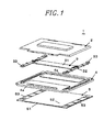
- An organic EL module 1 is formed by accommodating in a casing a combined structure of a thin organic EL panel 5 and a circuit substrate 3 having power supply elements such as a power distribution pattern and the like in order to easily handle the organic EL panel or facilitates supply of power from the outside.
- the organic EL module 1 of the first embodiment includes a cover 2, the circuit substrate 3, the casing 4 and the organic EL panel 5, as shown in Fig. 1 .
- the cover 2 is insertion-fitted to the casing 4.
- the circuit substrate 3 is formed by connecting three long substrates in an H-shape when viewed from the top.
- a power circuit 31 is provided at a central substrate of the circuit substrate 3, and connectors 33 are respectively provided at four end portions of both outer substrates of the circuit substrate 3.
- the power circuit 31 and the connectors 33 are electrically connected to each other by wiring patterns formed on the substrates and wirings such as a power feed wire and the like.
- the power circuit 31 is disposed at the inner side of the circuit substrate 3, and the wirings 32 from the circuit substrate 3 to the electrode terminals 53 of the organic EL panel 5 are disposed at both outer substrates. Due to this configuration of the circuit substrate 3, the end portions of the circuit substrate 3 can become thin, and the organic EL module 1 itself can become thin.
- Each of the connectors 33 includes a transmission side connector and a reception side connector.
- the external power is input to the power circuit 31 via the reception side connector, and is output to the outside via the transmission side connector.
- the output of the power circuit 31 is supplied to the opposite electrode terminals 53 of the organic EL panel 5 via the wirings 32 such as a power feed wire and the like.
- the electrode terminals 53 are electrically connected to an anode electrode 52a and a cathode electrode 52c of the organic EL panel 5.
- the wirings 32 are connected by wire bonding to the electrode terminals 53 of the organic EL panel 5.
- the casing 4 accommodates the circuit substrate 3 and the organic EL panel 5 in the upper and lower sides thereof, respectively. Further, an extended portion 4a is protruded by a predetermined width w from a side surface (each of the opposite side surfaces in this embodiment) of the casing 4 where the electrode terminals 53 of the organic EL panel 5 are not disposed (see Fig. 4 ).
- the predetermined width w is wide enough (e.g., about 1 to 3 cm) for an operator to hold the extended portions 4a.
- the organic EL panel 5 includes a transparent substrate 51 made of a glass substrate, a plastic film or the like, a light emitting unit 52, and electrode terminals 53 to which power from the circuit substrate 3 is supplied.
- the light emitting unit 52 has an anode electrode layer 52a made of ITO (Indium Tin Oxide) or the like, a light emitting layer 52b made of an organic compound, and a cathode electrode layer 52c, e.g., a metal electrode.
- the light emitting unit 52 is airtightly sealed by a sealing material 54 made of sheet-shaped copper or the like, and the electrode terminals 53 are formed in a state where the anode electrode layer 52a and the cathode electrode layer 52c are partially exposed from the sealing material 54.
- the extended portions 4a protruding by the predetermined width are formed at the opposite sides of the casing 4, and light is emitted from the organic EL panel 5 as a light emitting surface.
- the electrode terminals 53 are provided at the opposite short sides of the substantially rectangular organic EL panel 5, and the extended portions 4a having a length t shorter than a length a of the long sides of the organic EL panel 5 are respectively formed at central portions of the opposite side surfaces of the casing 4 where the electrode terminals 53 of the organic EL panel 5 are not disposed.
- the length l of the extended portions 4a along the long sides of the organic EL panel 5 is shorter than the entire length a of the long sides of the organic EL panel 5.
- cutoff portions for positioning are respectively formed at the corner portions of the organic EL module 1.
- the organic EL modules 1 can be extremely easily arranged.
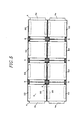
- the illumination device 7 shown in Fig. 6 includes the frame 8 to which a plurality of organic EL modules 1 are fitted and four organic EL modules 1. Moreover, the illumination device 7 receives power from a power supply unit (not shown) and serves as a lighting device using an organic EL light emitting device.
- the extended portions 4a formed at the casing 4 serve as handle portions, so that the operator can hold the extended portions 4a when handling the organic EL module 1. Accordingly, it is possible to protect the wirings 32 from damages caused when the operator holds the vicinity of the electrode terminals 53 and prevent contamination of the organic EL panel 5 with fingerprints. Besides, due to the shape of the extended portions 4a, the positioning of the organic EL modules 1 can be facilitated when the organic EL modules 1 are arranged in the frame 8 of the illumination device 7.
- the organic EL panel 5 is attached in the lower portion of the casing 4.
- the combined structure of the organic EL panel 5 and the circuit substrate 3 can be accommodated in a rectangular parallelepiped casing having a transparent light transmitting unit for transmitting light emitted from the organic EL panel 5.
- the power circuit 31 is provided at the circuit substrate 3.
- a power circuit provided separately from the organic EL module may be connected by a suitable electrical connection unit to the circuit substrate 3 of the organic EL module which has a wiring pattern formed thereon.
- the extended portions 4a are formed at both sides of the casing 4 in the present embodiment, the extended portion 4a may be formed at one side of the casing 4.
- FIG. 7 An organic EL module in accordance with a second embodiment of the present invention will be described with reference to Fig. 7 .
- extended portions 10a are formed at the side surfaces of the casing 4 where the electrode terminals 53 of the organic EL panel 5 are not disposed over the entire length thereof. Accordingly, a length a of the long sides of the organic EL panel 5 becomes equal to a width b of the casing 4, and the organic EL module 9 has a substantially square shape when viewed from the top.
- the damages to the wirings 32 or the contamination of the organic EL panel 5 with fingerprints can be prevented.
- the design feature is improved because a plurality of organic EL modules 9 arranged in the illumination device has a substantially square shape when viewed from the top.
- FIG. 8 An organic EL module 11 in accordance with a third embodiment of the present invention will be described with reference to Figs. 8 and 9 .
- extended portions 12a having a predetermined width are formed at both end portions of each side surface of a casing 12 where the electrode terminals 53 of the organic EL panel 5 are not disposed 2.
- the length (l1+l2) of the extended portions 12a along the long sides of the organic EL panel 5 is shorter than the entire length a of the long sides of the organic EL panel 5.
- the extended portions 12a and 14a can be engaged with each other like a puzzle, and the positioning of a plurality of organic EL modules can be facilitated.
- the extended portions 12a can serve as handle portions used for an operator to handle the organic EL module 11 and facilitate the positioning of a plurality of organic EL modules forming the illumination device.
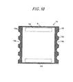
- FIG. 10 An organic EL module in accordance with a fourth embodiment of the present invention will be described with reference to Fig. 10 .
- a plurality of recesses 16b that are curved to match the shape of fingers to allow an operator to easily hold the organic EL module 15 are formed at extended portions 16a of a casing 16 along the long sides of the organic EL panel 5.
- This configuration not only provides the aforementioned effects but also allows an operator to extremely easily handle the organic EL module 15 by using the recesses 16b.
- FIG. 11 An organic EL module in accordance with a fifth embodiment of the present invention will be described with reference to Fig. 11 .
- cutoff portions 54 are respectively formed at the corner portions of an organic EL panel 5.
- the cutoff portion 54 may be formed at one or more corner portions of the organic EL panel 5, and the organic EL module 17 may have a substantially square shape when viewed from the top.
- the cutoff portion 54 is formed at each of the corner portions of the organic EL panel 5, so that the corner portions of a casing 18 where the cutoff portion 54 is disposed serve as handle portions. Since an operator can use the corner portions of the casing 18 as the handle portions, damages to the wirings 32 or contamination of the organic EL panel 5 with fingerprints can be prevented. Moreover, the extended portions of the casing 18 can be reduced or omitted and, thus, an area of a non-light-emitting portion of the organic EL module 17 which does not emit light can be reduced.
- the organic EL module of the present invention is not limited to those of the above embodiments, and can be variously modified without departing from the scope of the present invention.
- the organic EL light emitting device is used as a light emitting device in the above embodiments, the present invention can be applied to, e.g., an inorganic EL panel, a light emitting diode, a lighting device that is turned on by a DC current.
- the electrode terminals 53 connected to the anode electrode layer 52a and the cathode electrode layer 52c are provided at the opposite sides of the organic EL panel 5.
- the electrode terminal 53 may be provided at one side of the organic EL panel 5.
- the extended portions 4a may be at least partially formed at the sides of the organic panel where the electrode terminal 53 is not disposed.
- the electrode terminals 53 are provided at the short sides of the organic EL panel 5.
- the electrode terminals 53 may be provided at the long sides of the organic EL panel 5.
- the organic EL panel 5 has a rectangular shape in the above embodiments, the organic EL panel may have various shapes other than the rectangular shape.
Landscapes
- Physics & Mathematics (AREA)
- Optics & Photonics (AREA)
- Electroluminescent Light Sources (AREA)
- Fastening Of Light Sources Or Lamp Holders (AREA)
Applications Claiming Priority (1)
| Application Number | Priority Date | Filing Date | Title |
|---|---|---|---|
| JP2010088752A JP5559586B2 (ja) | 2010-04-07 | 2010-04-07 | 有機elモジュール |
Publications (2)
| Publication Number | Publication Date |
|---|---|
| EP2375862A2 true EP2375862A2 (de) | 2011-10-12 |
| EP2375862A3 EP2375862A3 (de) | 2017-11-29 |
Family
ID=44117072
Family Applications (1)
| Application Number | Title | Priority Date | Filing Date |
|---|---|---|---|
| EP11002891.7A Withdrawn EP2375862A3 (de) | 2010-04-07 | 2011-04-06 | Organisches EL-Modul und Beleuchtungsvorrichtung |
Country Status (4)
| Country | Link |
|---|---|
| US (1) | US8339035B2 (de) |
| EP (1) | EP2375862A3 (de) |
| JP (1) | JP5559586B2 (de) |
| CN (1) | CN102223740B (de) |
Cited By (1)
| Publication number | Priority date | Publication date | Assignee | Title |
|---|---|---|---|---|
| EP2634474A4 (de) * | 2010-10-25 | 2018-01-17 | Panasonic Intellectual Property Management Co., Ltd. | Lichtemittierendes modul |
Families Citing this family (12)
| Publication number | Priority date | Publication date | Assignee | Title |
|---|---|---|---|---|
| USD684126S1 (en) * | 2011-08-30 | 2013-06-11 | Panasonic Corporation | Electroluminescence module assembly |
| USD684125S1 (en) * | 2011-08-30 | 2013-06-11 | Panasonic Corporation | Electroluminescence module |
| USD684547S1 (en) * | 2011-08-30 | 2013-06-18 | Panasonic Corporation | Fixing base for an electroluminescence module |
| USRE45712E1 (en) * | 2013-03-18 | 2015-10-06 | Photonics Electronics Technology Research Association (PETRA) | Signal conversion device |
| USRE45741E1 (en) * | 2013-03-18 | 2015-10-13 | Photonics Electronics Technology Research Association (PETRA) | Signal conversion device |
| USD707193S1 (en) * | 2013-09-16 | 2014-06-17 | Photonics Electronics Technology Research Association (PETRA) | Signal conversion device |
| USD706733S1 (en) * | 2013-09-16 | 2014-06-10 | Photonics Electronics Technology Research Association (PETRA) | Signal conversion device |
| JP2017062870A (ja) * | 2014-02-10 | 2017-03-30 | パナソニックIpマネジメント株式会社 | 平面発光体、平面発光モジュール及び照明装置 |
| US9615409B2 (en) * | 2014-02-13 | 2017-04-04 | Kaneka Corporation | Light emission module, connector, and mounting structure for light emission module |
| WO2017187819A1 (ja) * | 2016-04-28 | 2017-11-02 | 株式会社キルトプランニングオフィス | 照明装置及び取付部材 |
| WO2019202739A1 (ja) * | 2018-04-20 | 2019-10-24 | 堺ディスプレイプロダクト株式会社 | 有機elデバイスおよびその製造方法 |
| JP1642346S (de) * | 2019-03-20 | 2019-09-30 |
Citations (1)
| Publication number | Priority date | Publication date | Assignee | Title |
|---|---|---|---|---|
| JP2003257617A (ja) | 2002-02-27 | 2003-09-12 | Ricoh Co Ltd | 機能性素子基板および該機能性素子基板を用いた画像表示装置 |
Family Cites Families (16)
| Publication number | Priority date | Publication date | Assignee | Title |
|---|---|---|---|---|
| JP2001085158A (ja) * | 1999-09-10 | 2001-03-30 | Toyota Central Res & Dev Lab Inc | 有機電界発光素子 |
| JP2003157023A (ja) * | 2001-11-22 | 2003-05-30 | Toshiba Corp | 表示装置、液晶表示装置およびエレクトロルミネッセンス表示装置 |
| US6787990B2 (en) * | 2002-05-28 | 2004-09-07 | Eastman Kodak Company | OLED area illumination light source having flexible substrate on a support |
| JP2004259656A (ja) * | 2003-02-27 | 2004-09-16 | Seiko Epson Corp | 表示モジュール及び電子機器 |
| JP2005128040A (ja) * | 2003-10-21 | 2005-05-19 | Hitachi Displays Ltd | 表示装置 |
| JP4679921B2 (ja) * | 2005-02-15 | 2011-05-11 | 小泉産業株式会社 | El光源体およびel光源装置 |
| KR20060113219A (ko) * | 2005-04-30 | 2006-11-02 | (주)에스엔제이인터내셔널 | 유기전계발광장치 |
| JP4487868B2 (ja) * | 2005-06-27 | 2010-06-23 | パナソニック電工株式会社 | 面発光パネルおよび照明装置 |
| KR100645694B1 (ko) * | 2005-12-21 | 2006-11-15 | 삼성에스디아이 주식회사 | 유기발광 표시장치 |
| JP4860530B2 (ja) * | 2006-04-04 | 2012-01-25 | コイズミ照明株式会社 | El光源体 |
| JP4924108B2 (ja) * | 2007-03-06 | 2012-04-25 | 船井電機株式会社 | 液晶パネル固定構造及び液晶テレビジョン |
| WO2008126250A1 (ja) * | 2007-03-30 | 2008-10-23 | Pioneer Corporation | 発光装置 |
| KR100857689B1 (ko) * | 2007-05-23 | 2008-09-08 | 삼성에스디아이 주식회사 | 유기 전계 발광표시장치 |
| JP4950809B2 (ja) * | 2007-08-22 | 2012-06-13 | パナソニック株式会社 | 照明器具 |
| JP2009146646A (ja) * | 2007-12-12 | 2009-07-02 | Nec Lighting Ltd | 平面光源ユニットおよびこれを用いた照明装置 |
| KR100918061B1 (ko) * | 2008-01-14 | 2009-09-22 | 삼성모바일디스플레이주식회사 | 유기발광 표시장치 |
-
2010
- 2010-04-07 JP JP2010088752A patent/JP5559586B2/ja not_active Expired - Fee Related
-
2011
- 2011-04-06 EP EP11002891.7A patent/EP2375862A3/de not_active Withdrawn
- 2011-04-07 CN CN201110094642.9A patent/CN102223740B/zh not_active Expired - Fee Related
- 2011-04-07 US US13/081,611 patent/US8339035B2/en not_active Expired - Fee Related
Patent Citations (1)
| Publication number | Priority date | Publication date | Assignee | Title |
|---|---|---|---|---|
| JP2003257617A (ja) | 2002-02-27 | 2003-09-12 | Ricoh Co Ltd | 機能性素子基板および該機能性素子基板を用いた画像表示装置 |
Cited By (1)
| Publication number | Priority date | Publication date | Assignee | Title |
|---|---|---|---|---|
| EP2634474A4 (de) * | 2010-10-25 | 2018-01-17 | Panasonic Intellectual Property Management Co., Ltd. | Lichtemittierendes modul |
Also Published As
| Publication number | Publication date |
|---|---|
| US20110248627A1 (en) | 2011-10-13 |
| CN102223740B (zh) | 2014-10-08 |
| US8339035B2 (en) | 2012-12-25 |
| CN102223740A (zh) | 2011-10-19 |
| EP2375862A3 (de) | 2017-11-29 |
| JP2011222223A (ja) | 2011-11-04 |
| JP5559586B2 (ja) | 2014-07-23 |
Similar Documents
| Publication | Publication Date | Title |
|---|---|---|
| US8339035B2 (en) | Organic EL module and illumination device including same | |
| JP4860530B2 (ja) | El光源体 | |
| US8764209B2 (en) | Light module | |
| EP2838317B1 (de) | Organisches elektrolumineszentes modul und stromversorgungsstruktur für das organische elektrolumineszente modul | |
| KR20200085835A (ko) | 터치 디스플레이 패널, 플렉서블 디스플레이 장치 및 터치 디스플레이 패널을 제조하는 방법 | |
| US7071618B2 (en) | Electroluminescent element comprising electrically coupled shield layer | |
| CN104012188A (zh) | 发光器件装置 | |
| CN103081575B (zh) | 在电路板上的光源装置和具有多个光源装置的光源设备 | |
| KR100604685B1 (ko) | 유기 전계 발광 소자, 그 제조 방법 및 조명 장치 | |
| US20150295202A1 (en) | OLED Lighting Panel and Methods for Fabricating Thereof | |
| US10756279B2 (en) | Display module | |
| US9013096B2 (en) | Light emitting module | |
| JP4432846B2 (ja) | 照明装置および照明器具 | |
| JP2005158372A (ja) | エレクトロルミネセンス素子及び照明装置 | |
| JP5081877B2 (ja) | 接続法が選択可能な発光モジュール | |
| JP2013065523A (ja) | 有機発光パネルおよびそれを用いた照明装置 | |
| JP2005345935A (ja) | 有機el表示器 | |
| US9853239B2 (en) | Surface light-emitting unit | |
| WO2020085368A1 (ja) | Oled照明装置 | |
| US10077890B2 (en) | Light-emitting device | |
| JP2007287345A (ja) | El発光モジュール | |
| KR20160055142A (ko) | 복사선 방출 장치 및 그 제조 방법 | |
| US20140111084A1 (en) | Oled lighting device | |
| US9559315B2 (en) | Surface light-emitting element and light-emitting device | |
| WO2014192543A1 (ja) | 面状発光パネルおよび電子機器 |
Legal Events
| Date | Code | Title | Description |
|---|---|---|---|
| PUAI | Public reference made under article 153(3) epc to a published international application that has entered the european phase |
Free format text: ORIGINAL CODE: 0009012 |
|
| AK | Designated contracting states |
Kind code of ref document: A2 Designated state(s): AL AT BE BG CH CY CZ DE DK EE ES FI FR GB GR HR HU IE IS IT LI LT LU LV MC MK MT NL NO PL PT RO RS SE SI SK SM TR |
|
| AX | Request for extension of the european patent |
Extension state: BA ME |
|
| RAP1 | Party data changed (applicant data changed or rights of an application transferred) |
Owner name: PANASONIC CORPORATION |
|
| 17P | Request for examination filed |
Effective date: 20140331 |
|
| RBV | Designated contracting states (corrected) |
Designated state(s): AL AT BE BG CH CY CZ DE DK EE ES FI FR GB GR HR HU IE IS IT LI LT LU LV MC MK MT NL NO PL PT RO RS SE SI SK SM TR |
|
| RAP1 | Party data changed (applicant data changed or rights of an application transferred) |
Owner name: PANASONIC INTELLECTUAL PROPERTY MANAGEMENT CO., LT |
|
| PUAL | Search report despatched |
Free format text: ORIGINAL CODE: 0009013 |
|
| AK | Designated contracting states |
Kind code of ref document: A3 Designated state(s): AL AT BE BG CH CY CZ DE DK EE ES FI FR GB GR HR HU IE IS IT LI LT LU LV MC MK MT NL NO PL PT RO RS SE SI SK SM TR |
|
| AX | Request for extension of the european patent |
Extension state: BA ME |
|
| RIC1 | Information provided on ipc code assigned before grant |
Ipc: H05B 33/08 20060101AFI20171020BHEP |
|
| STAA | Information on the status of an ep patent application or granted ep patent |
Free format text: STATUS: THE APPLICATION IS DEEMED TO BE WITHDRAWN |
|
| 18D | Application deemed to be withdrawn |
Effective date: 20180530 |