EP2377149B1 - Transistor bipolaire à borne d'émetteur à ajustage automatique - Google Patents
Transistor bipolaire à borne d'émetteur à ajustage automatique Download PDFInfo
- Publication number
- EP2377149B1 EP2377149B1 EP09765091.5A EP09765091A EP2377149B1 EP 2377149 B1 EP2377149 B1 EP 2377149B1 EP 09765091 A EP09765091 A EP 09765091A EP 2377149 B1 EP2377149 B1 EP 2377149B1
- Authority
- EP
- European Patent Office
- Prior art keywords
- base
- region
- layer
- collector
- emitter
- Prior art date
- Legal status (The legal status is an assumption and is not a legal conclusion. Google has not performed a legal analysis and makes no representation as to the accuracy of the status listed.)
- Active
Links
Images







Classifications
-
- H—ELECTRICITY
- H10—SEMICONDUCTOR DEVICES; ELECTRIC SOLID-STATE DEVICES NOT OTHERWISE PROVIDED FOR
- H10D—INORGANIC ELECTRIC SEMICONDUCTOR DEVICES
- H10D10/00—Bipolar junction transistors [BJT]
- H10D10/01—Manufacture or treatment
- H10D10/021—Manufacture or treatment of heterojunction BJTs [HBT]
-
- H—ELECTRICITY
- H10—SEMICONDUCTOR DEVICES; ELECTRIC SOLID-STATE DEVICES NOT OTHERWISE PROVIDED FOR
- H10D—INORGANIC ELECTRIC SEMICONDUCTOR DEVICES
- H10D10/00—Bipolar junction transistors [BJT]
- H10D10/01—Manufacture or treatment
- H10D10/051—Manufacture or treatment of vertical BJTs
-
- H—ELECTRICITY
- H10—SEMICONDUCTOR DEVICES; ELECTRIC SOLID-STATE DEVICES NOT OTHERWISE PROVIDED FOR
- H10D—INORGANIC ELECTRIC SEMICONDUCTOR DEVICES
- H10D10/00—Bipolar junction transistors [BJT]
- H10D10/40—Vertical BJTs
- H10D10/421—Vertical BJTs having both emitter-base and base-collector junctions ending at the same surface of the body
-
- H—ELECTRICITY
- H10—SEMICONDUCTOR DEVICES; ELECTRIC SOLID-STATE DEVICES NOT OTHERWISE PROVIDED FOR
- H10D—INORGANIC ELECTRIC SEMICONDUCTOR DEVICES
- H10D10/00—Bipolar junction transistors [BJT]
- H10D10/80—Heterojunction BJTs
- H10D10/821—Vertical heterojunction BJTs
-
- H—ELECTRICITY
- H10—SEMICONDUCTOR DEVICES; ELECTRIC SOLID-STATE DEVICES NOT OTHERWISE PROVIDED FOR
- H10D—INORGANIC ELECTRIC SEMICONDUCTOR DEVICES
- H10D62/00—Semiconductor bodies, or regions thereof, of devices having potential barriers
- H10D62/10—Shapes, relative sizes or dispositions of the regions of the semiconductor bodies; Shapes of the semiconductor bodies
- H10D62/13—Semiconductor regions connected to electrodes carrying current to be rectified, amplified or switched, e.g. source or drain regions
- H10D62/133—Emitter regions of BJTs
-
- H—ELECTRICITY
- H10—SEMICONDUCTOR DEVICES; ELECTRIC SOLID-STATE DEVICES NOT OTHERWISE PROVIDED FOR
- H10D—INORGANIC ELECTRIC SEMICONDUCTOR DEVICES
- H10D62/00—Semiconductor bodies, or regions thereof, of devices having potential barriers
- H10D62/10—Shapes, relative sizes or dispositions of the regions of the semiconductor bodies; Shapes of the semiconductor bodies
- H10D62/13—Semiconductor regions connected to electrodes carrying current to be rectified, amplified or switched, e.g. source or drain regions
- H10D62/133—Emitter regions of BJTs
- H10D62/136—Emitter regions of BJTs of heterojunction BJTs
-
- H—ELECTRICITY
- H10—SEMICONDUCTOR DEVICES; ELECTRIC SOLID-STATE DEVICES NOT OTHERWISE PROVIDED FOR
- H10D—INORGANIC ELECTRIC SEMICONDUCTOR DEVICES
- H10D62/00—Semiconductor bodies, or regions thereof, of devices having potential barriers
- H10D62/10—Shapes, relative sizes or dispositions of the regions of the semiconductor bodies; Shapes of the semiconductor bodies
- H10D62/13—Semiconductor regions connected to electrodes carrying current to be rectified, amplified or switched, e.g. source or drain regions
- H10D62/137—Collector regions of BJTs
-
- H—ELECTRICITY
- H10—SEMICONDUCTOR DEVICES; ELECTRIC SOLID-STATE DEVICES NOT OTHERWISE PROVIDED FOR
- H10D—INORGANIC ELECTRIC SEMICONDUCTOR DEVICES
- H10D62/00—Semiconductor bodies, or regions thereof, of devices having potential barriers
- H10D62/10—Shapes, relative sizes or dispositions of the regions of the semiconductor bodies; Shapes of the semiconductor bodies
- H10D62/17—Semiconductor regions connected to electrodes not carrying current to be rectified, amplified or switched, e.g. channel regions
- H10D62/177—Base regions of bipolar transistors, e.g. BJTs or IGBTs
-
- H—ELECTRICITY
- H10—SEMICONDUCTOR DEVICES; ELECTRIC SOLID-STATE DEVICES NOT OTHERWISE PROVIDED FOR
- H10D—INORGANIC ELECTRIC SEMICONDUCTOR DEVICES
- H10D62/00—Semiconductor bodies, or regions thereof, of devices having potential barriers
- H10D62/80—Semiconductor bodies, or regions thereof, of devices having potential barriers characterised by the materials
- H10D62/83—Semiconductor bodies, or regions thereof, of devices having potential barriers characterised by the materials being Group IV materials, e.g. B-doped Si or undoped Ge
- H10D62/832—Semiconductor bodies, or regions thereof, of devices having potential barriers characterised by the materials being Group IV materials, e.g. B-doped Si or undoped Ge being Group IV materials comprising two or more elements, e.g. SiGe
-
- H—ELECTRICITY
- H10—SEMICONDUCTOR DEVICES; ELECTRIC SOLID-STATE DEVICES NOT OTHERWISE PROVIDED FOR
- H10D—INORGANIC ELECTRIC SEMICONDUCTOR DEVICES
- H10D84/00—Integrated devices formed in or on semiconductor substrates that comprise only semiconducting layers, e.g. on Si wafers or on GaAs-on-Si wafers
- H10D84/01—Manufacture or treatment
- H10D84/0107—Integrating at least one component covered by H10D12/00 or H10D30/00 with at least one component covered by H10D8/00, H10D10/00 or H10D18/00, e.g. integrating IGFETs with BJTs
- H10D84/0109—Integrating at least one component covered by H10D12/00 or H10D30/00 with at least one component covered by H10D8/00, H10D10/00 or H10D18/00, e.g. integrating IGFETs with BJTs the at least one component covered by H10D12/00 or H10D30/00 being a MOS device
-
- H—ELECTRICITY
- H10—SEMICONDUCTOR DEVICES; ELECTRIC SOLID-STATE DEVICES NOT OTHERWISE PROVIDED FOR
- H10D—INORGANIC ELECTRIC SEMICONDUCTOR DEVICES
- H10D84/00—Integrated devices formed in or on semiconductor substrates that comprise only semiconducting layers, e.g. on Si wafers or on GaAs-on-Si wafers
- H10D84/01—Manufacture or treatment
- H10D84/0112—Integrating together multiple components covered by H10D8/00, H10D10/00 or H10D18/00, e.g. integrating multiple BJTs
-
- H—ELECTRICITY
- H10—SEMICONDUCTOR DEVICES; ELECTRIC SOLID-STATE DEVICES NOT OTHERWISE PROVIDED FOR
- H10D—INORGANIC ELECTRIC SEMICONDUCTOR DEVICES
- H10D84/00—Integrated devices formed in or on semiconductor substrates that comprise only semiconducting layers, e.g. on Si wafers or on GaAs-on-Si wafers
- H10D84/01—Manufacture or treatment
- H10D84/02—Manufacture or treatment characterised by using material-based technologies
- H10D84/03—Manufacture or treatment characterised by using material-based technologies using Group IV technology, e.g. silicon technology or silicon-carbide [SiC] technology
- H10D84/038—Manufacture or treatment characterised by using material-based technologies using Group IV technology, e.g. silicon technology or silicon-carbide [SiC] technology using silicon technology, e.g. SiGe
Definitions
- the invention relates to a bipolar semiconductor device having one or more vertical bipolar transistors having an emitter, a base and a collector region, wherein the usual T-shaped emitter laterally overlaps the base terminal region laterally adjoining the base. Furthermore, the invention relates to a method for producing such a bipolar semiconductor device.
- bipolar transistors Bipolar Junction Transistor, BJT
- BJT Bipolar Junction Transistor
- Known embodiments include highly conductive base and collector termination regions that dissipate the charge carrier current from the inner transistor region to the corresponding contact regions.
- a high conductivity is achieved by a locally well-controlled doping and in at least one embodiment by a monocrystalline base connection region.
- the semiconductor regions are characterized by insulator regions with a low dielectric constant, for. B. by silica, separated from each other. The resulting overlaps of the emitter and collector regions with the base are kept as small as possible, which is achieved in particular by self-aligned method.
- bipolar transistors bipolar junction transistor, BJT
- BJT bipolar junction transistor
- the document US 2001/0017399 A1 shows a bipolar transistor with n-doped collector and emitter regions and an intervening intrinsic base region.
- the base region and adjacent regions of the emitter region and the collector region are made of Si 0.7 Ge 0.3 .
- emitter and collector regions are made of silicon.
- Laterally adjacent to the intrinsic base region is a p-doped SiGe interconnect layer on which a p + doped polysilicon interconnect layer rests.
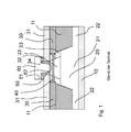
- Fig. 1 shows in a cross-sectional view of a bipolar transistor according to the prior art, which in its essential features the transistor of the Fig. 1 (a) from the cited publication by Washio.
- a collector region 20 is adjacent to a substrate 10 and laterally (laterally) to silicon dioxide (SiO 2 ) filled recesses 11 in the silicon, which are also called field isolation regions.
- SiO 2 silicon dioxide
- STI shallow trenches
- the collector region 20 is composed of a substrate-side, highly doped collector region 21 and an overlying, low-doped collector region Collector area 23 together.
- the collector region is adjoined in the lateral direction under the STI regions 11 by sections 22 of a collector connection region.
- a collector window 34 is produced in a layer stack consisting of a first insulator layer 30, a polysilicon layer 31 and a second insulator layer 32.
- a portion of the polysilicon layer 31 protruding laterally beyond the first insulator region 30 is produced at the lateral edge of the window 34.
- the end faces of the overhanging portions of the polysilicon layer 31 are provided with Abtandshaltern, so-called spacers 50 made of insulator material.
- silicon fronts grow vertically from the exposed portions of the polysilicon layer 31 and the collector region 20 and close the gap between the polysilicon layer 31 serving as part of the base pad region and the inner transistor region.
- a T-shaped emitter region 60 abuts the bottom of the base layer 40 and laterally of the spacers 50 with a vertical portion corresponding to the vertical T-bar.
- a cap layer is deposited over the SiGe layer, which can pick up dopant dopants from the emitter in the manufacturing process and can accommodate at least part of the base-emitter space charge zone.
- the emitter-side boundary of the cap layer is indicated by a dashed dividing line in the emitter. Portions of the emitter 60 corresponding to the horizontal T-bar lie laterally on the second insulator layer 32.
- SIC region 33 a selectively implanted collector region, also referred to as SIC region 33 (in which the collector doping is locally raised), to simultaneously control the collector-base transit time, the base To minimize collector capacitance and collector resistance in a manner that enables good high speed transistor characteristics.
- Fig. 2 shows in a cross-sectional view of another vertical bipolar transistor according to the prior art. Schematically illustrated is a section of the inner transistor region and the adjacent base and collector terminal regions.
- the transistor of Fig. 2 has a single-polysilicon differential-deposited base structure. Significant features of the collector design are consistent with those of the double polysilicon variant of Fig. 1 match.
- a collector 120 is enclosed downwardly from a substrate 110 and toward the sides of STI regions 111. On the substrate side, the collector 120 has a highly doped portion 121. Towards the surface, the collector has a low-doped portion 123.
- polycrystalline semiconductor material 130 is deposited in the single polysilicon variant during the differential epitaxial step for base fabrication on the field isolation regions, which may be used as part of the base termination region.
- an SIC region 133 is used.
- the known single-polysilicon transistor designs typically exhibit weaker doped silicon regions in side-by-side proximity to the SIC region 133, which cause undesirable capacitance contributions between the base-junction and collector regions.
- the emitter is T-shaped as in the double-polysilicon variant, with the width of the overlap 161 being adjusted photolithographically beyond the emitter window 162 as well as in double-polysilicon technology.
- Fig. 3 shows in a cross section a third bipolar transistor according to the prior art. Schematically illustrated is a section of the inner transistor region and the adjacent base and collector terminal regions.
- the transistor of Fig. 3 has a single ended polysilicon differential-ended structure that faces the transistor of FIG Fig. 2 allows the formation of a single-crystal base terminal region and has a reduced parasitic base-collector capacitance due to the special design of the collector region.
- a collector 220 is enclosed downwardly from a substrate 210 and toward the sides of STI regions 211. On the substrate side, the collector 220 has a heavily doped portion 221.
- the transistor has a first semiconductor electrode of monocrystalline semiconductor material of a second conductivity type arranged in an opening of the isolation region, which is designed either as a collector or as an emitter, and which has a first height section, which encloses the isolation region in a lateral direction perpendicular to the height direction is and has an adjacent, in the height direction of the substrate interior further away second height portion which is not laterally enclosed by the isolation area.
- the transistor has a second semiconductor electrode of semiconductor material of the second conductivity type, which is formed as the other type of semiconductor electrode, ie as an emitter or alternatively as a collector, a base of monocrystalline semiconductor material of the first conductivity type between the collector and the emitter, and a base terminal region, the a monocrystalline portion laterally surrounding the base and the second height portion of the first semiconductor electrode farther from the base farther to the substrate interior, and the bottom side facing the substrate interior rests directly on the isolation region, and vertical isolated single-crystal base connection region section, VIEBAG section briefly is called.
- the emitter window 262 is positioned self-aligned with respect to the base terminal region and with respect to the SIC, while that extending beyond the emitter window 262 Width of the overlap 261 of the emitter with the base terminal 230 is adjusted by photolithographic methods.
- Fig. 4 shows in a cross section a fourth bipolar transistor according to the prior art. Schematically illustrated is a section of the inner transistor region and the adjacent base and collector terminal regions.
- the transistor of Fig. 4 has a differential-deposited base design characterized by extensive use of self-aligned techniques.
- a collector 320 is bounded downwardly by a substrate 310.
- the collector 320 is led via a connection region 321 under the isolation region 311 to the collector contact region 322.
- the transistor is formed in a window of a base connection region made of polysilicon 331, which is opened over the region of the collector 320.
- a monocrystalline base layer stack 307 and a lightly doped cover layer 308 are deposited over the collector region, during which time a polycrystalline compound 310 is formed on the sidewalls of the base connection region.
- L-shaped spacers 350 also formed in the interior of the window in the base terminal region 331 separate the emitter 360 from the base terminal region 331.
- the entire emitter is self-aligned in this embodiment to the opening in the base terminal region.
- the width of the region of the T-shaped emitter 360 projecting beyond the emitter window 362 and separated from a base connection region 309 by the lower part of the spacers 350 is for opening in the base connection region 331 and thus also to the emitter window 362 through the L-shaped spacers 350 set.
- the length of the base terminal region which has a significant portion of the base resistance, is directly related to the width of the horizontal region of the T-shaped emitter.
- the emitter can not be designed and optimized independently of the base connection region.
- the location and extent of the T-shaped emitter are also adjusted in known manufacturing processes by the use of a photolithographically positioned mask. As a result, the overlap dimension can not be designed without considering the error tolerances associated with the photolithographic process.
- the parasitic resistance of the base terminal could also be reduced in this way by allowing highly conductive areas of the base terminal to be brought closer to the inner base with a small overlap than is possible in the prior art.
- Such areas are, for example, silicide, an epitaxial amplification of the base terminal or an additional implantation of the base terminal used to increase the doping.
- the known transistor arrangements shown have a second critical aspect: the parts of the base terminal lying on insulator area consist in Fig. 1 . 2 and 4 made of polycrystalline material, whereby contact and lead resistances compared to values for monocrystalline material are significantly increased.
- the base terminal is made of monocrystalline material.
- the technical problem underlying the invention is therefore to provide a semiconductor device for vertical bipolar transistors in which improved properties for high-speed applications are achieved by reducing or completely avoiding the described disadvantages of known embodiments, in particular with regard to parasitic capacitances and resistances.
- a further technical problem underlying the invention is to specify a method for producing a bipolar semiconductor device with which the described disadvantages of known methods, in particular with regard to parasitic capacitances and resistances, can be reduced or completely avoided.
- the semiconductor device according to the invention is characterized by particularly good high-frequency characteristics of its bipolar transistor. These are achieved by a reduced resistance of the base connection region, which is accompanied by a particularly small parasitic base-emitter capacitance of the bipolar transistor due to the structure according to the invention, in particular when using the method described below process control.
- the base connection area represents an area with particularly good conductivity.
- the base connection region apart from a seed layer adjacent to the substrate and / or a metallization layer adjoining a base contact, consists of a semiconductor material that is made of the semiconductor material of the collector, the base and the emitter is different in chemical composition and has a higher mobility of majority charge carriers of the first conductivity type in comparison with this.
- the material thus has increased hole mobility and, in the case of an n-conductive base connection region, increased electron mobility.
- the bipolar transistor according to the invention has due to the inventive possibility described below of a self-aligned production of the lateral overlap of the emitter with the base terminal region.
- the overlap area can be made smaller. Due to the smaller overlap of the crossbar of the T-shaped emitter highly conductive portions of the base terminal region can be brought particularly close to the inner transistor. These highly conductive portions may be, for example, siliconized regions, epitaxial gains of the base lead region, or regions doped higher by implantation.
- this advantage can also be achieved if the base connection region is made of the same material as the functional layers of the inner transistor.
- the base terminal region of a vertical bipolar transistor is significantly improved in terms of its high-frequency characteristics.
- the material of the base connection region is preferably silicon germanium with a germanium content of more than 35%, ie Si 1-x Ge x , where x is at least 0.35. Silicon germanium with such a high germanium content is characterized by a significantly higher hole mobility compared to silicon. In this way, with materials that are compatible with known industrial manufacturing processes, a particularly low resistance in the base terminal region can be achieved. An even greater effect in this direction can be achieved by using silicon germanium with a germanium content of more than 50%, or even better, even more than 80% for the base terminal region.
- Germanium has even a factor of about 10 increased hole mobility. Even compared to the common variants of silicon germanium, which have a relatively low germanium content, germanium has a significantly increased hole conductivity.
- the comparison of the hole conductivities of different materials refers to at least approximately the same dopant concentrations and for this purpose only those dopant concentration values come into consideration, which are within a value range of interest for transistor fabrication.
- the base terminal region may be wholly or partly monocrystalline in different embodiments of the semiconductor device.
- the base terminal region can contain two subareas, of which only one first subarea directly adjacent to the base is monocrystalline, but a second is polycrystalline.
- An at least partially monocrystalline base terminal region provides improved conductivity compared to polycrystalline material.
- monocrystalline we refer to sections which have a uniform crystallographic orientation, which is predetermined either by the substrate or corresponds to one of the other highly symmetrical surface orientations, in the case of silicon the surface orientations (100), (110), (111) or (311) .
- polycrystalline regions are those regions consisting of a plurality of crystallites having different crystallographic orientations which are contiguous in grain boundaries and may have extents ranging from a few nanometers to a few hundred nanometers.
- a buffer layer of monocrystalline semiconductor material is arranged between the collector and the base.
- a cover layer of monocrystalline semiconductor material can be arranged between the base and the emitter.
- the emitter is T-shaped, whose horizontal T-bar overlaps outwardly with the respective base connection region, over the total number of these bipolar transistors of the semiconductor device has an overlap with a variation of its lateral extent of at most 10 nanometers.
- Such a homogeneous structure with respect to the overlap can be achieved by the method of the invention, which will be explained below.
- a self-adjusted adjustment of the overlap width of the horizontal T-beam of the emitter is achieved with the base terminal region.
- Self-aligned in this context means that the lateral positioning or structural expansion of an area with respect to already produced areas is not done via the adjustment of a photolithographic mask, but the already prepared areas themselves specify the positioning and, possibly provided with spacers, serve as a mask for process steps. This eliminates positional errors and defines dimensions such as distances of regions from one another by well controllable processes such as layer depositions, which altogether permits a significant reduction in distances and dimensions in comparison to regions positioned above one another by means of photolithography.
- the method according to the invention can be carried out in particular in such a way that the base connection region is made of a semiconductor material that apart from the semiconductor material of the collector, the base (apart, if appropriate) from a seed layer adjacent to the substrate or a metallization layer adjacent to a base contact and the emitter is different in chemical composition and has a higher mobility of majority carriers of the first conductivity type as compared therewith.
- a seed layer can be used to improve the crystalline properties of the base connection region, as known per se, in particular when producing a monocrystalline base connection region. However, it is not mandatory.
- a metallization layer can also be fabricated without prior coverage of the base pad region with an additional semiconductor layer, such as silicon to produce a metallization layer of titanium silicide or cobalt silicide.
- an additional semiconductor layer such as silicon
- germanium for example, it is possible to produce a nickel silicide layer without prior deposition of a silicon layer prior to formation of the silicide.
- the method advantageously starts the deposition of the layer stack from a high-resistance monocrystalline semiconductor substrate of the first conductivity type, which in previous process steps with the first height section of a collector region of the second conductivity type laterally bounded by a first isolation region.
- the layer stack is produced, in the direction of layer growth, either comprising the following layer combination or consisting of the following layer combination: a second insulation region, a polycrystalline or amorphous semiconductor layer, an insulation layer, a first auxiliary layer and a second auxiliary layer.
- the layer stack is produced, in the direction of the layer growth, either comprising the following layer combination or consisting of the following layer combination: a second insulation region, a first auxiliary layer, a second auxiliary layer and a third auxiliary layer.
- the formation of the window in the layer stack is preferably carried out such that the window in the lateral area of the collector extends from the second auxiliary layer in the depth direction to the interface between the semiconductor layer and the second insulation area. This allows a subsequent access to the second isolation region for the production of the second height portion of the collector base stack in the inner transistor region.
- the lateral extent of a SIC region which is preferably formed in a subsequent implantation step, can be set in the upper height section of the collector.
- the implantation of the SIC area can basically be done before or after deposition of a base stack in the window.
- the base stack consists in one embodiment of a buffer layer, a base layer and a cover layer.
- the deposition is now preferably carried out selectively in such a way that at the same time on the side wall of the semiconductor layer, a polycrystalline inner region of the base connection region is formed. This can be achieved, for example, by attacking the spacers during partial removal from below, so that they are completely removed in sections in the region of the semiconductor layer.
- the production of the cavity can be achieved in one embodiment by lateral, selective etching back of the first auxiliary layer in the region of the window, so that a laterally extending beyond the window lateral cavity of the first auxiliary layer is formed.
- the deposition of the T-shaped emitter in the window and in the cavity of the first auxiliary layer is therefore subsequently carried out in a self-aligned manner, wherein in particular the width of the over the lateral extent of the window protruding lateral overlap of the emitter with the base terminal region by the width of the back etching of first auxiliary layer in a self-aligned manner according to the invention.
- the formation of the window in the layer stack is also preferably carried out here such that the window extends in the lateral area of the collector area in the depth direction up to its first height section. Subsequently, preferably a selective epitaxial deposition of a second height section of the collector in the region of the window and a base stack.
- the base stack consists in one embodiment in the growth direction of a buffer layer, a base layer and a cover layer. The growth of the layer stack is preferably carried out so far that the base layer stack in the growth direction reaches at most to the bottom of the first auxiliary layer.
- a selective, lateral etching back of the second auxiliary layer in the region of the window is then preferably carried out, so that a laterally extending beyond the window side cavity of the second auxiliary layer is formed.
- the deposition of the T-shaped emitter in the window and in the cavity of the second auxiliary layer following in a self-aligned manner in turn, in particular the width of over the lateral extent of the window protruding lateral overlap of the emitter with the base terminal region by the width of the back etching in self-aligned manner results.
- a higher layer thickness of the base connection region can be achieved outwardly than in the inner region, whereby the resistance of the base connection region can be reduced.
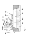
- FIG. 5 shows a cross-sectional view of this first example.
- a vertical npn bipolar transistor is fabricated on a high-resistance, single-crystal p - type Si substrate 410.
- the arrangement described here is not limited to p - -conductive Si substrates.
- the essential features can also be transferred to substrates of the opposite conductivity type.
- CMOS transistors may be present on the substrate 410 at the same time, but are in FIG. 5 not shown.
- the vertical npn bipolar transistor of Fig. 5 includes an n-type bottom collector region 420, which forms a first height portion of a collector of the bipolar transistor, and a likewise n-type emitter 460.
- the collector is laterally connected to a collector contact region 422 via a collector connection region 421.
- Contact structures such as emitter base and collector contact are in Fig. 5 For the sake of simplicity of presentation, it is not shown graphically.
- a single-crystal layer stack is arranged, which includes an upper collector region 405 as a second height portion of the collector, a base layer stack 407 consisting of a buffer layer 407a and the base layer 407b, and a cap layer 408.
- the second height portion of the collector 405 is formed by selective epitaxial growth on the collector 420 in the region of a window in the insulating layer 430 and may have a thickness of 5 nm to 200 nm, preferably 60 nm to 150 nm.
- the second height section 405 is n-doped. Outside the inner region 406, the second height section 405 is weakly n- or weakly p-doped.
- the n-type dopant in the inner region 406 is made by ion implantation.
- the inner area is also called the SIC area.
- the base layer stack 407 initially contains a buffer layer 407a. This layer may be 5 nm to 120 nm, preferably 30 nm to 70 nm thick. Above the buffer layer, the p-type base layer 407b is formed. The thickness of the base layer may be 5 nm to 100 nm, preferably 10 nm to 50 nm. Over the base layer stack is a 5 nm to 100 nm, preferably 10 nm to 50 nm thick cover layer 408, which is also prepared by selective epitaxial growth.
- the base 407 may preferably be incorporated in an alloy of SiGe.
- carbon may have been incorporated in the buffer layer 407a, in the base layer 407b, or in the cap layer 408 during epitaxy.
- a polycrystalline layer with base connection regions 432 and 431 adjoins layers 407 and 408 toward the outside.
- the inner base terminal region 432 is formed during the epitaxial growth of the layers 407 and 408 and has a lateral extension of 5 nm to 150 nm and a vertical extension of 5 nm to 150 nm.
- the outer base terminal region 431 has a thickness of 20 nm to 200 nm, preferably 50 nm to 150 nm.
- a first type of isolation regions 411 projects into the interior of the substrate and laterally bounds the lower collector region 420.
- field isolation regions so-called “shallow-trench” isolations, as are known from CMOS technologies, can be used. These are preferably 250 to 600 nm deep trenches z. B. with silicon dioxide (SiO 2 ), but also with a combination of insulator material and polysilicon can be filled. Alternatively, field isolation regions produced by means of local oxidation (LOCOS) can also be used. In addition to the flat field isolation areas are also deep, z. B. with SiO 2 filled trenches, so-called “deep trenches", usable, however, in the arrangement according to Fig. 5 are not provided.
- LOCOS local oxidation
- the first insulating layer 430 is 20 nm to 200 nm thick and partially rests on the isolation region 411 and partially on the collector 420.
- the insulating layer is preferably made of an insulator material with a low dielectric constant. For this purpose, silicon dioxide (SiO 2 ), but also another, so-called low-k material can be used.
- a second structured insulation layer 451 This may preferably consist of a 10 nm to 150 nm, preferably 30 nm to 120 nm thick SiO 2 layer. But it can also be composed of a combination of different insulator materials.
- An approximately L-shaped spacer 450 made of insulating material ensures the electrical insulation of the emitter 460 from the base connection region 431 and 432.
- the exact Profile of the spacer is not exactly L-shaped, as can be seen from the figures.
- the spacer could be described in more detail as a Z-shaped or double-L-shaped, but is referred to here in the professional habituation habituation here as L-shaped, without making a commitment to the exact L-shape.
- the aperture formed over the capping layer 408 by the spacers 450 defines the emitter window 462.
- a highly doped collector-type silicon layer, the npn emitter layer 460 covers the emitter window, the spacers 450, and the insulator layer 451.
- the npn emitter layer 460 may be referred to polycrystalline, amorphous, partially monocrystalline, partially polycrystalline or deposited as monocrystalline material and is polycrystalline in the final state, monocrystalline or in some areas monocrystalline or polycrystalline.
- n-dopant may be diffused into the cap layer 408 through the emitter window during a high-temperature step, as indicated by an arcuate line in the cap layer 408 directly below the emitter.
- the emitter in this case comprises the npn emitter layer 460 and the diffused n-type region.
- conductive silicide layers are formed compared to highly doped Si.
- the surface of the transistor and isolation regions is finally covered with an insulator layer or layer combination. Vias filled with conductive material and overlying metal strips provide electrical connection to the contact regions of the transistor.
- FIGS. 6 to 12 a method for producing the semiconductor device according to the invention as described above in this example.
- the basis for the production forms a substrate 410 (FIG. Figure 6 ), which preferably comprises a very high-impedance, single-crystalline p-type (low p-type doping) silicon.
- the processing process of the substrate 410 begins with the generation of the field isolation regions 411. In the present example so-called “shallow trenches" are used as field isolation regions. Islands of Si areas formed between the field isolation areas form active areas. The active region will accommodate the collector region 420, collector junction region 421, and collector contact region 422 upon completion of the vertical bipolar transistor.
- the doping of the collector region 420 is introduced after completion of the field isolation regions by ion implantation in the silicon.
- Fig. 6 shows a snapshot during the fabrication of the bipolar transistor.
- Field isolation regions 411 and collector region 420 are already made.
- a layer stack in this embodiment consisting of an insulation layer 430, which forms a second insulation region, a semiconductor layer 431, a further insulation layer 401, a first auxiliary layer 402 and a second auxiliary layer 403 has been produced which covers the entire wafer.
- the insulating layer 401 preferably consists of SiO 2 and is 20 nm to 200 nm, preferably 80 nm to 120 nm thick.
- the semiconductor layer 431 preferably consists of polycrystalline, p-doped silicon and is 20 nm to 200 nm, preferably 80 nm to 120 nm thick.
- the insulating layer 401 is preferably made of SiO 2 and is 10 nm to 100 nm, preferably 30 nm to 70 nm thick.
- the first auxiliary layer 402 preferably consists of Si 3 N 4 and is 100 nm to 200 nm, preferably 130 nm to 170 nm thick.
- the second auxiliary layer 403 is preferably made of SiO 2 and is 150 to 250, preferably 170 nm to 210 nm thick. For all layer thicknesses, it should be noted that they can not be selected independently of one another or from other process parameters, especially those of etching processes.
- the second auxiliary layer 403 can be dispensed with in favor of a higher layer thickness of the first auxiliary layer 402.
- the initial layer thickness of the first auxiliary layer should then take into account the ablation rate of the first auxiliary layer in an etch process described below to form a window 400 and in an etch process to form a lateral cavity in the first auxiliary layer in the region of the window.
- an existing second auxiliary layer 403 is assumed.
- a window is produced in the layers 403, 402, 401 and 431.
- the last dry etch process is ideally designed so that the etch selectively etches the layer 431 to SiO 2 and thus stops the etch on the isolation layer 430.
- spacers 404 are now produced by layer deposition and subsequent anisotropic dry etching. The moment immediately after the generation of the spacer is in Fig. 7 shown.
- the width of the spacers is 50 nm to 130 nm, preferably 70 nm to 110 nm.
- the second isolation area 430 will also be opened. This is preferably done by a combination of dry and wet chemical etching.
- the dry etching removes most of the material in an anisotropic manner.
- the surface of the silicon of the collector 420 is exposed by wet-chemical etching.
- the wet-chemical etching is to be preferred for this purpose, as it protects the silicon surface during exposure because of high selectivity and the exclusion of radiation damage.
- the openable layer 430 from a layer stack consisting of two layers, wherein the combination of layer materials and etchant are chosen so that a lower of the two layers in the wet chemical etching process used a larger etch rate than an upper of the two Has layers.
- the isotropic wet chemical etching produces a profile, as in Figure 8 is indicated. In this profile, the opening in the layer 430 down, so in a direction towards the substrate interior, wider. This profile may have advantages for the finished transistor in terms of lower collector resistance at low collector-base capacitance.
- auxiliary layer 403 is also affected by the etching of the layer 430 and the layer removal must be taken into account when setting the output layer thickness.
- a monocrystalline semiconductor layer 405 is formed on the exposed silicon surface of the collector in the region of the transistor window opening by selective epitaxial growth.
- This layer is 5 nm to 200 nm, preferably 60 nm to 150 nm thick. Selective growth means that no material deposition occurs on the materials making up the spacers 404 and auxiliary layer 403.
- an inner region 406 of the layer 405 is n-doped.
- Figure 8 is a snapshot shown at this point of manufacturing.
- An outer region adjacent to the n-doped inner region becomes effective of capacity advantages, preferably weakly n-doped or weakly p-doped. This is typically done immediately upon deposition of the layer 405.
- the spacers 404 are now partially removed from the side wall of the semiconductor layer 431 facing the inside of the window. In a lower portion of the semiconductor layer 431, the spacers are completely removed in this step.
- the thickness of the grown layer 405 can be selected or its surface subsequently retracted so that the spacers are also attacked from below in an etching process.
- a polycrystalline inner base connection region 432 is thus created simultaneously, which establishes the connection of the outer base connection region 431 to the base 407b.
- the manufacturing stage after the epitaxial deposition process is in Fig. 9 shown.
- the spacers 404 are completely removed and furthermore the auxiliary layer 402 is removed laterally, so that a cavity is formed between the layers 401 and 403.
- the depth of this cavity in the lateral direction which can be adjusted by the duration of the etching process, determines the subsequent overlap of the emitter contact 460 with the base terminal region 431. The overlap is thus positioned self-aligned with the remaining areas of the bipolar transistor generated in the transistor window.
- the moment after the wet chemical etching is in Fig. 10 shown.
- Spacers consisting of a first spacer layer 450 and a second spacer layer 409, are now generated again in the interior of the transistor window by layer deposition and subsequent, largely anisotropic etching.
- the last step of the etch that exposes the surface of the cap 408 is preferably accomplished by a wet chemical etch to preserve the surface of the cap layer 408.
- the material of the second spacer layer 409 should be chosen so that it can later be selectively removed to the first spacer layer 450 in an isotropic etching process.
- the second spacer layer 409 constitutes an auxiliary layer which generates the L-shaped configuration of the first spacer layer 450, which is advantageous for the function of the bipolar transistor is.
- the first spacer layer 450 preferably consists of SiO 2 and is 20 nm to 80 nm, preferably 50 nm to 70 nm thick.
- the second spacer layer 409 is preferably made of Si 3 N 4 and is 50nm to 130nm, preferably 70nm to 110nm thick. The moment after the wet-chemical exposure of the surface of the cap layer 408 is in Fig. 11 shown.
- the second spacer layer 409 is now removed by a wet chemical etching process. Then, an n-type semiconductor layer which forms the later emitter 460 is deposited.
- the deposition can either as a selective deposition of a single crystal layer, as deposition of a polycrystalline layer, as differential deposition, the monocrystalline material on the cover layer 408 and in all other areas generated polycrystalline material, or as a differential deposition on the cover layer 408 monocrystalline and on all amorphous material is generated in all other areas.
- CMP chemical mechanical polishing
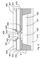
- the auxiliary layer 403 is also removed by the CMP step and subsequent etching steps for cleaning the wafer surface. This moment of manufacturing is in Fig. 12 shown.
- the auxiliary layer 401, the insulation layer 401 and the base connection region 431 are patterned with the aid of a photolithographically produced resist mask so that the base connection region is given its final shape.
- the structuring takes place by means of customary dry etching processes.
- the auxiliary layer 402 is removed in a wet-chemical etching process selectively with respect to the exposed SiO 2 and Si layers.
- the insulating layer 401 is removed from the surface of the base connection region and the insulating layer 430 is removed from the surface of the colector contact region 422 in a preferably anisotropic dry etching process which removes the SiO 2 as selectively as possible against the exposed silicon regions, for example that of the emitter.
- bipolar transistor by the generation of a high n-type doping (not shown) in the region of the Kolektor contact region 422, preferably by ion implantation, the production of a silicide (not shown) for reducing parasitic resistance components in the emitter, base and collector contact areas (not shown), and finally the production of a contact by metal contacts (not shown) completed connecting the bipolar transistor with a separated by an insulating layer interconnect system.
- FIG. 13 shows a cross-sectional view of this embodiment.
- Fig. 21 shows a variant of the embodiment. It will be in the FIGS. 13 to 21 , which refer to the two variants of the example, for the same structural elements the same reference numerals as in the example of Fig. 5 to 12 used.
- FIGS. 14 to 20 a method for producing the semiconductor device according to the invention as described above in this embodiment explained.
- the basis for the production forms a substrate 410 (FIG. Figure 14 ), which preferably comprises a high-impedance, single-crystal p - -conducting (low p-type doping) silicon.
- the processing process of the substrate 410 begins with the generation of the field isolation regions 411. In the present example so-called “shallow trenches" are used as field isolation regions. Islands of Si areas formed between the field isolation areas form active areas. The active region will receive the collector 420, collector junction region 421 and collector contact region 422 upon completion of the vertical bipolar transistor.
- the doping of the collector 420 is introduced after completion of the field isolation regions by ion implantation in the silicon.
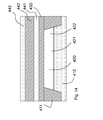
- Fig. 14 shows a snapshot during the fabrication of the bipolar transistor.
- Field isolation regions 411 and collector lower heights 420 are already made.
- a layer stack consisting of the insulation layer 430, a first auxiliary layer 441, a second auxiliary layer 442 and a third auxiliary layer 443 has been produced.
- the insulating layer 401 is preferably made of SiO 2 and is 20 nm to 150 nm, preferably 80 nm to 120 nm thick.
- the first auxiliary layer 441 preferably consists of Si 3 N 4 and is 20 nm to 150 nm, preferably 50 nm to 120 nm thick.
- the second auxiliary layer 442 is preferably made of SiO 2 and is 50 nm to 250 nm, preferably 130nm to 170nm thick.
- the third auxiliary layer 443 preferably consists of Si 3 N 4 and is 50 nm to 100 nm, preferably 60 nm to 80 nm thick.
- a window defined by a photolithographic process is now produced in the layers 443, 442, 441 and 430, cf. Fig. 15 .
- the profile can be adjusted so that the transistor window becomes wider towards the substrate.
- the auxiliary layers 441 and 443 if they protrude significantly further into the transistor window after the wet-chemical etching than the layers 430 and 442, can be pulled back by a further wet-chemical etching process.
- the single crystal semiconductor layer 405, the base stack 407, and the cap layer 408 are formed by selective epitaxial growth in the region of the transistor window on the first height portion 420 of the collector, cf. Fig. 16 , Growth may be interrupted in the meantime for implantation of SIC area 406.
- a later implantation through the grown base stack is also possible.
- the SIC area 406 is in the present embodiment, only in the later stage of the method Fig. 18 drawn without, however, excluding the variant of a previous implantation as described.
- the auxiliary layer 442 is then laterally retracted by a wet-chemical etching process, so that a hollow is created between the layers 441 and 443, cf. Fig. 17 .
- the lateral expansion of this cavity which can be adjusted for a given etch solution by the duration of the etch process, determines the later lateral extent of the emitter contact 460 overlap with the base pad 431.
- the lateral extent of this overlap is thus self-aligned to the transistor window and thus also positioned to the other areas of the bipolar transistor generated in the transistor window.
- the L-shaped spacers 450 and the emitter 460 are generated analogously to Example 1, by first a spacer consisting of a SiO 2 and a Si 3 N 4 layer at the Inner wall of the transistor window are generated, the Si 3 N 4 is removed and the emitter 460 is polycrystalline, monocrystalline or partly monocrystalline and partly polycrystalline generated, either by selective growth or by a combination of polycrystalline deposition or differential deposition with a CMP step. The auxiliary layer 443 is then removed. This moment of manufacturing is in Fig. 15 shown.
- auxiliary layer 444 preferably consisting of SiO 2 and 30 nm to 100 nm, preferably 40 nm to 60 nm thick.
- the layers 444 and 442 are patterned by conventional dry etching processes, so that they predetermine the shape of the later base connection region.
- the auxiliary layer 441 is now removed laterally below the layer 442 selectively with respect to all other layers present, so that the side wall of the base layer stack 407 is exposed. This condition is in Fig. 19 shown.
- the base connection region 431 is generated. This is preferably done by selective epitaxial growth. However, it may also be prepared by depositing an amorphous layer which is made crystalline by thermal treatment. This state of manufacture is in Fig. 20 shown.
- FIG. 21 Another variant of the design of the base connection area is in Fig. 21 shown.
- the distance between the layers 430 and 442 can be increased by an isotropic etching, before a further region 431b, which may be monocrystalline or polycrystalline, is produced.
- the silicon which has developed outside the actual base connection region is removed by a dry etching process, which selectively removes the silicon from SiO 2 .
- the base terminal region remains protected by the layer 442, which serves as a mask for the etch.
- a subsequent etching process which removes SiO 2 selectively to silicon, removes the SiO 2 layers covering the emitter, base, and collector contact regions. Through this process one arrives at a cross section as it is in Fig. 13 is shown.
- the bipolar transistor is finally completed by generating a high n-type doping in the region of the collector contact 422, preferably by ion implantation, the generation of a silicide to reduce parasitic resistance levels in the emitter, base and collector contact regions, and finally the formation of a contact by metal contacts, which connect the bipolar transistor to a conductive track system separated from it by an insulating layer.
- the structures are rotated 45 degrees from a conventional deposition about an axis perpendicular to the substrate surface, thereby providing advantages in the selective growth of Si, ultimately improving the high speed characteristics of the bipolar transistor.
- the semiconductor device may include, in addition to bipolar transistors, other semiconductor devices fabricated in MOS or CMOS technology.
- bipolar transistors other semiconductor devices fabricated in MOS or CMOS technology.
- the above description of the figures was limited to the example of npn bipolar transistors.
- the invention is not limited thereto.
- a bipolar transistor of a semiconductor device according to the invention can be embodied either as an npn transistor or as a pnp transistor.
- the person skilled in the art can resort to the material parameters of the electron and hole mobility of potential semiconductor materials published in standard works.
Landscapes
- Bipolar Transistors (AREA)
Claims (11)
- Dispositif semi-conducteur, comprenant une couche de substrat (410) constituée d'un matériau semi-conducteur d'un premier type de conductivité avec une première zone d'isolation (411) et un transistor bipolaire vertical avec- une première portion de hauteur d'un collecteur (420), disposée dans une ouverture de la première zone d'isolation (411), constituée d'un matériau semi-conducteur d'un deuxième type de conductivité,- une deuxième zone d'isolation (430), qui s'appuie en partie sur la première portion de hauteur du collecteur (420) et en partie sur la première zone d'isolation (411) et présente, au niveau du collecteur, une ouverture dans laquelle se trouve une deuxième portion de hauteur (405) du collecteur en matériau monocristallin, qui comprend une zone interne (406) du deuxième type de conductivité,- une base (407b) constituée d'un matériau semi-conducteur monocristallin du premier type de conductivité,- une zone de connexion de base (431) qui entoure la base (407b) dans la direction latérale,- un émetteur en forme de T (460) en matériau semi-conducteur du deuxième type de conductivité, qui chévauche la zone de connexion de base (431),caractérisé en ce que la zone de connexion de base, excepté la couche d'ensemencement ou la couche de métallisation, est soit partiellement soit entièrement monocristalline et en ce que la zone de connexion de base (431), excepté une couche d'ensemencement adjacente au substrat ou une couche de métallisation adjacente à un contact de base, est constituée d'un matériau semi-conducteur différent du matériau semi-conducteur du collecteur (402, 405), de la base et de l'émetteur (460) du point de vue de sa composition chimique et présente, par rapport à celui-ci, une mobilité plus élevée des porteurs de charges majoritaires du premier type de conductivité.
- Dispositif semi-conducteur selon la revendication 1, dans lequel le matériau de la zone de connexion de base est du silicium-germanium avec une part de germanium supérieure à 35%.
- Dispositif semi-conducteur selon la revendication 1 ou 2, dans lequel le matériau de la zone de connexion de base est du germanium, tandis que le matériau du collecteur, de la base et de l'émetteur est du silicium ou du siliciumgermanium.
- Dispositif semi-conducteur selon la revendication 1, dans lequel la zone de connexion de base contient deux zones partielles (431a, 431b) dont une première zone partielle (431a), directement adjacente à la base (407b), est monocristalline.
- Dispositif semi-conducteur selon la revendication 4, dans lequel une deuxième zone partielle (431b) de la zone de connexion de base présente une épaisseur verticale supérieure à la première zone partielle (432a).
- Dispositif semi-conducteur selon l'une des revendications précédentes, avec une pluralité de transistors bipolaires verticaux avec les caractéristiques du transistor bipolaire de la revendication 1, dans lesquels l'émetteur est en forme de T, la barre horizontale se superposant, vers l'extérieur, avec la zone de connexion de base et l'extension latérale de cette superposition présente une variation de 10 nanomètres maximum sur l'ensemble de ces transistors bipolaires du dispositif semi-conducteur.
- Procédé de fabrication d'un transistor bipolaire vertical dans lequel- dans une pile de couches, déposée en partie sur une première portion de hauteur d'un collecteur (420), constituée d'un matériau semi-conducteur monocristallin et en partie sur une zone d'isolation (411) entourant celle-ci, une fenêtre est réalisée dans la zone latérale du collecteur,- dans la fenêtre, une deuxième portion de hauteur (405) du collecteur et une pile de base (407) sont déposées de manière monocristalline,- une zone de connexion de base (431), reliée latéralement à la pile de base, est réalisée,- dans au moins une couche de la pile de couches, située au-dessus de la pile de base, est réalisé un évidement latéral s'étendant latéralement au-delà de la fenêtre et- un émetteur en forme de T est réalisé en remplissant l'évidement latéral, une extension latérale de la barre horizontale du T et sa superposition latérale avec la zone de connexion de base étant prédéterminée par l'évidement latéral,la zone de connexion de base (431), excepté une couche d'ensemencement adjacente au substrat ou une couche de métallisation adjacente à un contact de base, est constituée soit partiellement soit entièrement d'un matériau monocristallin différent du matériau semi-conducteur du collecteur (420, 405), de la base et de l'émetteur (460) du point de vue de sa composition chimique et présente, par rapport à celui-ci, une mobilité plus élevée des porteurs de charges majoritaires du premier type de conductivité.
- Procédé selon la revendication 7, dans lequel la zone de connexion de base est constituée de silicium-germanium, avec une part de germanium d'au moins 35%, ou de germanium.
- Procédé selon l'une des revendications 7 ou 8, dans lequel la pile de couches, en direction de la croissance des couches, contient la combinaison de couches suivante ou est constitué de la combinaison de couches suivante : une deuxième zone d'isolation (430), une première couche auxiliaire (441), une deuxième couche auxiliaire (442) et une troisième couche auxiliaire (443).
- Procédé selon la revendication 9, comprenant en outre :- dépôt de l'émetteur en forme de T (460) dans la fenêtre (400a) et dans l'évidement de la deuxième couche auxiliaire, la largeur de la superposition latérale de l'émetteur (460) avec la zone de connexion de base (431) dépassant de l'extension latérale de la fenêtre (400) étant définie par la largeur de gravure de retour de manière auto-ajustable.
- Procédé selon l'une des revendications 9 ou 10, dans lequel seule une partie de la zone de connexion de base présente d'abord une croissance épitactique sélective puis la distance verticale entre la couche d'isolation (430) et la deuxième couche auxiliaire (442) est agrandie par gravure isotrope puis la partie restante de la zone de connexion de base est produite par épitaxie sélective ou différentielle.
Priority Applications (1)
| Application Number | Priority Date | Filing Date | Title |
|---|---|---|---|
| EP14188533.5A EP2830097B1 (fr) | 2008-12-12 | 2009-12-03 | Transistor bipolaire doté de contact émetteur à ajustage automatique et son procédé de fabrication |
Applications Claiming Priority (3)
| Application Number | Priority Date | Filing Date | Title |
|---|---|---|---|
| DE102008054576 | 2008-12-12 | ||
| DE102009001552A DE102009001552A1 (de) | 2008-12-12 | 2009-03-13 | Bipolartransistor mit selbstjustiertem Emitterkontakt |
| PCT/EP2009/066316 WO2010066630A1 (fr) | 2008-12-12 | 2009-12-03 | Transistor bipolaire à borne d'émetteur à ajustage automatique |
Related Child Applications (2)
| Application Number | Title | Priority Date | Filing Date |
|---|---|---|---|
| EP14188533.5A Division-Into EP2830097B1 (fr) | 2008-12-12 | 2009-12-03 | Transistor bipolaire doté de contact émetteur à ajustage automatique et son procédé de fabrication |
| EP14188533.5A Division EP2830097B1 (fr) | 2008-12-12 | 2009-12-03 | Transistor bipolaire doté de contact émetteur à ajustage automatique et son procédé de fabrication |
Publications (2)
| Publication Number | Publication Date |
|---|---|
| EP2377149A1 EP2377149A1 (fr) | 2011-10-19 |
| EP2377149B1 true EP2377149B1 (fr) | 2015-09-30 |
Family
ID=42168798
Family Applications (2)
| Application Number | Title | Priority Date | Filing Date |
|---|---|---|---|
| EP14188533.5A Active EP2830097B1 (fr) | 2008-12-12 | 2009-12-03 | Transistor bipolaire doté de contact émetteur à ajustage automatique et son procédé de fabrication |
| EP09765091.5A Active EP2377149B1 (fr) | 2008-12-12 | 2009-12-03 | Transistor bipolaire à borne d'émetteur à ajustage automatique |
Family Applications Before (1)
| Application Number | Title | Priority Date | Filing Date |
|---|---|---|---|
| EP14188533.5A Active EP2830097B1 (fr) | 2008-12-12 | 2009-12-03 | Transistor bipolaire doté de contact émetteur à ajustage automatique et son procédé de fabrication |
Country Status (4)
| Country | Link |
|---|---|
| US (2) | US8933537B2 (fr) |
| EP (2) | EP2830097B1 (fr) |
| DE (1) | DE102009001552A1 (fr) |
| WO (1) | WO2010066630A1 (fr) |
Families Citing this family (45)
| Publication number | Priority date | Publication date | Assignee | Title |
|---|---|---|---|---|
| EP2458623B1 (fr) | 2010-11-26 | 2014-06-25 | Nxp B.V. | Procédé de fabrication d'un transistor bipolaire et transistor bipolaire |
| EP2466628A1 (fr) | 2010-12-16 | 2012-06-20 | Nxp B.V. | Procédé de fabrication de transistor bipolaire et transistor bipolaire |
| EP2555235B1 (fr) | 2011-08-02 | 2014-06-18 | Nxp B.V. | Procédé de fabrication de CI comportant plusieurs transistors bipolaires et CI comportant plusieurs transistors bipolaires |
| EP2581930B1 (fr) | 2011-10-11 | 2014-06-04 | Nxp B.V. | Procédé de fabrication de transistor bipolaire, transistor bipolaire et circuit intégré |
| EP2565911B1 (fr) | 2011-09-02 | 2014-08-20 | Nxp B.V. | Procédé de fabrication de CI comportant un transistor bipolaire et CI |
| CN102412286B (zh) * | 2011-11-03 | 2014-05-21 | 上海华虹宏力半导体制造有限公司 | 一种高速锗硅hbt器件结构及其制造方法 |
| US8610174B2 (en) * | 2011-11-30 | 2013-12-17 | International Business Machines Corporation | Bipolar transistor with a raised collector pedestal for reduced capacitance |
| FR2989514A1 (fr) * | 2012-04-11 | 2013-10-18 | St Microelectronics Sa | Procede de fabrication d'un transistor bipolaire |
| US9245951B1 (en) * | 2014-09-16 | 2016-01-26 | Globalfoundries Inc. | Profile control over a collector of a bipolar junction transistor |
| DE102014113989B4 (de) | 2014-09-26 | 2020-06-04 | Infineon Technologies Ag | Verfahren zur Herstellung eines Bipolartransistors |
| DE102015204411B4 (de) * | 2015-03-11 | 2020-11-05 | Infineon Technologies Dresden Gmbh | Transistor und Verfahren zur Herstellung eines Transistors |
| DE102015208133B3 (de) | 2015-04-30 | 2016-08-18 | Infineon Technologies Ag | BiMOS-Vorrichtung mit einem vollständig selbstausgerichteten Emittersilicium und Verfahren zu deren Herstellung |
| US9425269B1 (en) | 2015-06-23 | 2016-08-23 | Globalfoundries Inc. | Replacement emitter for reduced contact resistance |
| FR3047838A1 (fr) * | 2016-02-16 | 2017-08-18 | St Microelectronics Sa | Transistor bipolaire et son procede de fabrication |
| FR3050867B1 (fr) | 2016-05-02 | 2018-05-25 | Commissariat A L'energie Atomique Et Aux Energies Alternatives | Procede de fabrication d'un transistor a nanocouches a canal vertical |
| US9847408B1 (en) * | 2016-06-21 | 2017-12-19 | Globalfoundries Inc. | Fabrication of integrated circuit structures for bipolor transistors |
| US10032868B2 (en) * | 2016-09-09 | 2018-07-24 | Texas Instruments Incorporated | High performance super-beta NPN (SBNPN) |
| US9786770B1 (en) | 2016-10-06 | 2017-10-10 | Nxp Usa, Inc. | Semiconductor device structure with non planar slide wall |
| US10134880B2 (en) | 2017-03-29 | 2018-11-20 | Globalfoundries Inc. | Self-aligned bipolar junction transistors with a base grown in a dielectric cavity |
| US10367084B2 (en) | 2017-07-31 | 2019-07-30 | Globalfoundries Inc. | Cascode heterojunction bipolar transistors |
| US10186605B1 (en) | 2017-10-13 | 2019-01-22 | Stmicroelectronics (Crolles 2) Sas | Cyclic epitaxy process to form air gap isolation for a bipolar transistor |
| US10224423B1 (en) | 2017-10-13 | 2019-03-05 | STMircoelectronics (Crolles 2) SAS | Heterojunction bipolar transistor and method of manufacturing the same |
| EP3547371B1 (fr) | 2018-03-27 | 2025-10-15 | NXP USA, Inc. | Transistor bipolaire et procédé de fabrication d'un transistor bipolaire |
| US10777668B2 (en) | 2018-08-21 | 2020-09-15 | Globalfoundries Inc. | Bipolar junction transistors with a self-aligned emitter and base |
| FR3087048B1 (fr) | 2018-10-08 | 2021-11-12 | St Microelectronics Sa | Transistor bipolaire |
| FR3087047B1 (fr) | 2018-10-08 | 2021-10-22 | St Microelectronics Sa | Transistor bipolaire |
| FR3098016A1 (fr) | 2019-06-28 | 2021-01-01 | Stmicroelectronics (Crolles 2) Sas | Procédé de réalisation d’une diode |
| FR3098015A1 (fr) | 2019-06-28 | 2021-01-01 | Stmicroelectronics (Crolles 2) Sas | Procédé de réalisation d’une diode |
| US11195925B2 (en) | 2019-09-23 | 2021-12-07 | Globalfoundries U.S. Inc. | Heterojunction bipolar transistors |
| US11171210B2 (en) | 2019-10-11 | 2021-11-09 | Globalpoundries U.S. Inc. | Double mesa heterojunction bipolar transistor |
| US11018247B1 (en) | 2019-12-26 | 2021-05-25 | Nxp Usa, Inc. | Semiconductor device with a base link region and method therefor |
| FR3107783A1 (fr) * | 2020-02-28 | 2021-09-03 | Stmicroelectronics (Crolles 2) Sas | Procédé de fabrication d’un transistor bipolaire et transistor bipolaire susceptible d’être obtenu par un tel procédé |
| FR3113539B1 (fr) | 2020-08-24 | 2022-09-23 | St Microelectronics Crolles 2 Sas | Transistor bipolaire |
| CN117941040A (zh) * | 2021-09-08 | 2024-04-26 | 华为技术有限公司 | 半导体结构及其制备方法、射频电路 |
| US11855173B2 (en) | 2021-12-15 | 2023-12-26 | Nxp Usa, Inc. | Transistor with monocrystalline base structures |
| EP4199064B1 (fr) * | 2021-12-16 | 2025-06-25 | IHP GmbH - Leibniz Institute for High Performance Microelectronics/ Leibniz-Institut für innovative Mikroelektronik | Procédé de fabrication de transistors bipolaires à épitaxie de base non sélective |
| US11855197B2 (en) | 2022-01-20 | 2023-12-26 | Globalfoundries U.S. Inc. | Vertical bipolar transistors |
| US11881523B2 (en) | 2022-05-10 | 2024-01-23 | Globalfoundries U.S. Inc. | Heterojunction bipolar transistors |
| FR3142035B1 (fr) * | 2022-11-10 | 2026-01-30 | St Microelectronics Sa | Procédé de fabrication d'un transistor |
| US12457784B2 (en) | 2022-12-14 | 2025-10-28 | Nxp B.V. | Semiconductor device with lateral base link region |
| US12538507B2 (en) | 2022-12-16 | 2026-01-27 | Nxp B.V. | Semiconductor device having an extrinsic base region with a monocrystalline region and method therefor |
| EP4428923A1 (fr) * | 2023-03-08 | 2024-09-11 | Nxp B.V. | Hbt sige et procedes de fabrication |
| FR3153688B1 (fr) * | 2023-10-02 | 2025-10-10 | St Microelectronics Int Nv | Procédé de fabrication d'un transistor bipolaire |
| US20260026275A1 (en) * | 2024-07-19 | 2026-01-22 | Texas Instruments Incorporated | Facet suppression for epitaxial growth |
| US12464746B1 (en) | 2024-11-13 | 2025-11-04 | Globalfoundries U.S. Inc. | Isolation stack for a bipolar transistor and related methods |
Family Cites Families (14)
| Publication number | Priority date | Publication date | Assignee | Title |
|---|---|---|---|---|
| DE58909837D1 (de) * | 1989-09-22 | 1998-09-17 | Siemens Ag | Verfahren zur Herstellung eines Bipolartransistors mit verminderter Basis/Kollektor-Kapazität |
| US5286661A (en) | 1992-08-26 | 1994-02-15 | Motorola, Inc. | Method of forming a bipolar transistor having an emitter overhang |
| US5516710A (en) * | 1994-11-10 | 1996-05-14 | Northern Telecom Limited | Method of forming a transistor |
| US6521974B1 (en) * | 1999-10-14 | 2003-02-18 | Hitachi, Ltd. | Bipolar transistor and manufacturing method thereof |
| DE10160509A1 (de) * | 2001-11-30 | 2003-06-12 | Ihp Gmbh | Halbleitervorrichtung und Verfahren zu ihrer Herstellung |
| DE10162074B4 (de) | 2001-12-06 | 2010-04-08 | Ihp Gmbh - Innovations For High Performance Microelectronics / Leibniz-Institut Für Innovative Mikroelektronik | BiCMOS-Struktur, Verfahren zu ihrer Herstellung und Bipolartransistor für eine BiCMOS-Struktur |
| WO2004090988A1 (fr) * | 2003-04-10 | 2004-10-21 | Infineon Technologies Ag | Procede de production d'un composant a semi-conducteur bipolaire, en particulier d'un transistor bipolaire, et composant a semi-conducteur bipolaire correspondant |
| DE10327709A1 (de) | 2003-06-21 | 2005-01-13 | Infineon Technologies Ag | Integrierte Schaltungsanordnung mit npn- und pnp-Bipolartransistoren sowie Herstellungsverfahren |
| JP2005094001A (ja) * | 2003-09-17 | 2005-04-07 | Stmicroelectronics Sa | 高いダイナミックパーフォーマンスを有するバイポーラトランジスタ |
| DE10358047A1 (de) | 2003-12-05 | 2005-06-30 | IHP GmbH - Innovations for High Performance Microelectronics/Institut für innovative Mikroelektronik | Komplementäre Bipolar-Halbleitervorrichtung |
| DE102004061327A1 (de) | 2004-12-11 | 2006-06-14 | IHP GmbH - Innovations for High Performance Microelectronics/Institut für innovative Mikroelektronik | Vertikaler Bipolartransistor |
| US7598539B2 (en) * | 2007-06-01 | 2009-10-06 | Infineon Technologies Ag | Heterojunction bipolar transistor and method for making same |
| US20090065804A1 (en) | 2007-09-10 | 2009-03-12 | International Business Machines Corporation | Bipolar transistor with low resistance base contact and method of making the same |
| US8405127B2 (en) * | 2008-02-20 | 2013-03-26 | International Business Machines Corporation | Method and apparatus for fabricating a heterojunction bipolar transistor |
-
2009
- 2009-03-13 DE DE102009001552A patent/DE102009001552A1/de not_active Withdrawn
- 2009-12-03 EP EP14188533.5A patent/EP2830097B1/fr active Active
- 2009-12-03 WO PCT/EP2009/066316 patent/WO2010066630A1/fr not_active Ceased
- 2009-12-03 EP EP09765091.5A patent/EP2377149B1/fr active Active
- 2009-12-03 US US12/998,869 patent/US8933537B2/en active Active
-
2014
- 2014-12-01 US US14/556,352 patent/US9508824B2/en active Active
Also Published As
| Publication number | Publication date |
|---|---|
| DE102009001552A1 (de) | 2010-06-17 |
| US9508824B2 (en) | 2016-11-29 |
| EP2377149A1 (fr) | 2011-10-19 |
| EP2830097B1 (fr) | 2021-02-24 |
| EP2830097A1 (fr) | 2015-01-28 |
| US8933537B2 (en) | 2015-01-13 |
| US20150140771A1 (en) | 2015-05-21 |
| US20120001192A1 (en) | 2012-01-05 |
| WO2010066630A1 (fr) | 2010-06-17 |
Similar Documents
| Publication | Publication Date | Title |
|---|---|---|
| EP2377149B1 (fr) | Transistor bipolaire à borne d'émetteur à ajustage automatique | |
| DE10308870B4 (de) | Bipolartransistor mit verbessertem Basis-Emitter-Übergang und Verfahren zur Herstellung | |
| EP1825504B1 (fr) | Transistor bipolaire vertical | |
| EP4199064B1 (fr) | Procédé de fabrication de transistors bipolaires à épitaxie de base non sélective | |
| EP1692720B1 (fr) | Dispositif semi-conducteur bipolaire complementaire | |
| EP1625614B1 (fr) | Procede de production d'un transistor bipolaire | |
| DE10358046B4 (de) | Bipolartransistor mit erhöhtem Basisanschlussgebiet und Verfahren zu seiner Herstellung | |
| EP1116278B1 (fr) | Transistor bipolaire et son procede de fabrication | |
| DE102015204411B4 (de) | Transistor und Verfahren zur Herstellung eines Transistors | |
| EP1454359B1 (fr) | Dispositif a semiconducteur et procede de fabrication dudit dispositif | |
| EP1611615A1 (fr) | Procede de production d'un composant a semi-conducteur bipolaire, en particulier d'un transistor bipolaire, et composant a semi-conducteur bipolaire correspondant | |
| DE102004053393B4 (de) | Verfahren zur Herstellung einer vertikal integrierten Kaskodenstruktur und vertikal integrierte Kaskodenstruktur | |
| EP1118124B1 (fr) | Transistor bipolaire et son procede de fabrication | |
| DE10249897B4 (de) | Selbstjustierendes Verfahren zur Herstellung eines Transistors | |
| WO2005098926A1 (fr) | Procede de production d'un transistor bipolaire dote d'une borne de base amelioree | |
| WO2000017932A1 (fr) | Transistor bipolaire et son procede de fabrication | |
| DE102004053394A1 (de) | Halbleiteranordnung und Verfahren zur Herstellung einer Halbleiteranordnung |
Legal Events
| Date | Code | Title | Description |
|---|---|---|---|
| PUAI | Public reference made under article 153(3) epc to a published international application that has entered the european phase |
Free format text: ORIGINAL CODE: 0009012 |
|
| 17P | Request for examination filed |
Effective date: 20110712 |
|
| AK | Designated contracting states |
Kind code of ref document: A1 Designated state(s): AT BE BG CH CY CZ DE DK EE ES FI FR GB GR HR HU IE IS IT LI LT LU LV MC MK MT NL NO PL PT RO SE SI SK SM TR |
|
| DAX | Request for extension of the european patent (deleted) | ||
| GRAP | Despatch of communication of intention to grant a patent |
Free format text: ORIGINAL CODE: EPIDOSNIGR1 |
|
| INTG | Intention to grant announced |
Effective date: 20150428 |
|
| GRAS | Grant fee paid |
Free format text: ORIGINAL CODE: EPIDOSNIGR3 |
|
| GRAA | (expected) grant |
Free format text: ORIGINAL CODE: 0009210 |
|
| AK | Designated contracting states |
Kind code of ref document: B1 Designated state(s): AT BE BG CH CY CZ DE DK EE ES FI FR GB GR HR HU IE IS IT LI LT LU LV MC MK MT NL NO PL PT RO SE SI SK SM TR |
|
| REG | Reference to a national code |
Ref country code: CH Ref legal event code: EP Ref country code: GB Ref legal event code: FG4D Free format text: NOT ENGLISH |
|
| REG | Reference to a national code |
Ref country code: AT Ref legal event code: REF Ref document number: 752869 Country of ref document: AT Kind code of ref document: T Effective date: 20151015 |
|
| REG | Reference to a national code |
Ref country code: IE Ref legal event code: FG4D Free format text: LANGUAGE OF EP DOCUMENT: GERMAN |
|
| REG | Reference to a national code |
Ref country code: DE Ref legal event code: R096 Ref document number: 502009011691 Country of ref document: DE |
|
| REG | Reference to a national code |
Ref country code: FR Ref legal event code: PLFP Year of fee payment: 7 |
|
| PG25 | Lapsed in a contracting state [announced via postgrant information from national office to epo] |
Ref country code: LV Free format text: LAPSE BECAUSE OF FAILURE TO SUBMIT A TRANSLATION OF THE DESCRIPTION OR TO PAY THE FEE WITHIN THE PRESCRIBED TIME-LIMIT Effective date: 20150930 Ref country code: FI Free format text: LAPSE BECAUSE OF FAILURE TO SUBMIT A TRANSLATION OF THE DESCRIPTION OR TO PAY THE FEE WITHIN THE PRESCRIBED TIME-LIMIT Effective date: 20150930 Ref country code: GR Free format text: LAPSE BECAUSE OF FAILURE TO SUBMIT A TRANSLATION OF THE DESCRIPTION OR TO PAY THE FEE WITHIN THE PRESCRIBED TIME-LIMIT Effective date: 20151231 Ref country code: LT Free format text: LAPSE BECAUSE OF FAILURE TO SUBMIT A TRANSLATION OF THE DESCRIPTION OR TO PAY THE FEE WITHIN THE PRESCRIBED TIME-LIMIT Effective date: 20150930 Ref country code: NO Free format text: LAPSE BECAUSE OF FAILURE TO SUBMIT A TRANSLATION OF THE DESCRIPTION OR TO PAY THE FEE WITHIN THE PRESCRIBED TIME-LIMIT Effective date: 20151230 |
|
| REG | Reference to a national code |
Ref country code: NL Ref legal event code: MP Effective date: 20150930 |
|
| REG | Reference to a national code |
Ref country code: LT Ref legal event code: MG4D |
|
| PG25 | Lapsed in a contracting state [announced via postgrant information from national office to epo] |
Ref country code: HR Free format text: LAPSE BECAUSE OF FAILURE TO SUBMIT A TRANSLATION OF THE DESCRIPTION OR TO PAY THE FEE WITHIN THE PRESCRIBED TIME-LIMIT Effective date: 20150930 Ref country code: SE Free format text: LAPSE BECAUSE OF FAILURE TO SUBMIT A TRANSLATION OF THE DESCRIPTION OR TO PAY THE FEE WITHIN THE PRESCRIBED TIME-LIMIT Effective date: 20150930 |
|
| PG25 | Lapsed in a contracting state [announced via postgrant information from national office to epo] |
Ref country code: SK Free format text: LAPSE BECAUSE OF FAILURE TO SUBMIT A TRANSLATION OF THE DESCRIPTION OR TO PAY THE FEE WITHIN THE PRESCRIBED TIME-LIMIT Effective date: 20150930 Ref country code: NL Free format text: LAPSE BECAUSE OF FAILURE TO SUBMIT A TRANSLATION OF THE DESCRIPTION OR TO PAY THE FEE WITHIN THE PRESCRIBED TIME-LIMIT Effective date: 20150930 Ref country code: IS Free format text: LAPSE BECAUSE OF FAILURE TO SUBMIT A TRANSLATION OF THE DESCRIPTION OR TO PAY THE FEE WITHIN THE PRESCRIBED TIME-LIMIT Effective date: 20160130 Ref country code: ES Free format text: LAPSE BECAUSE OF FAILURE TO SUBMIT A TRANSLATION OF THE DESCRIPTION OR TO PAY THE FEE WITHIN THE PRESCRIBED TIME-LIMIT Effective date: 20150930 Ref country code: CZ Free format text: LAPSE BECAUSE OF FAILURE TO SUBMIT A TRANSLATION OF THE DESCRIPTION OR TO PAY THE FEE WITHIN THE PRESCRIBED TIME-LIMIT Effective date: 20150930 Ref country code: EE Free format text: LAPSE BECAUSE OF FAILURE TO SUBMIT A TRANSLATION OF THE DESCRIPTION OR TO PAY THE FEE WITHIN THE PRESCRIBED TIME-LIMIT Effective date: 20150930 Ref country code: IT Free format text: LAPSE BECAUSE OF FAILURE TO SUBMIT A TRANSLATION OF THE DESCRIPTION OR TO PAY THE FEE WITHIN THE PRESCRIBED TIME-LIMIT Effective date: 20150930 |
|
| PG25 | Lapsed in a contracting state [announced via postgrant information from national office to epo] |
Ref country code: PT Free format text: LAPSE BECAUSE OF FAILURE TO SUBMIT A TRANSLATION OF THE DESCRIPTION OR TO PAY THE FEE WITHIN THE PRESCRIBED TIME-LIMIT Effective date: 20160201 Ref country code: RO Free format text: LAPSE BECAUSE OF FAILURE TO SUBMIT A TRANSLATION OF THE DESCRIPTION OR TO PAY THE FEE WITHIN THE PRESCRIBED TIME-LIMIT Effective date: 20150930 Ref country code: PL Free format text: LAPSE BECAUSE OF FAILURE TO SUBMIT A TRANSLATION OF THE DESCRIPTION OR TO PAY THE FEE WITHIN THE PRESCRIBED TIME-LIMIT Effective date: 20150930 Ref country code: BE Free format text: LAPSE BECAUSE OF NON-PAYMENT OF DUE FEES Effective date: 20151231 |
|
| REG | Reference to a national code |
Ref country code: DE Ref legal event code: R097 Ref document number: 502009011691 Country of ref document: DE |
|
| PG25 | Lapsed in a contracting state [announced via postgrant information from national office to epo] |
Ref country code: LU Free format text: LAPSE BECAUSE OF FAILURE TO SUBMIT A TRANSLATION OF THE DESCRIPTION OR TO PAY THE FEE WITHIN THE PRESCRIBED TIME-LIMIT Effective date: 20151203 Ref country code: MC Free format text: LAPSE BECAUSE OF FAILURE TO SUBMIT A TRANSLATION OF THE DESCRIPTION OR TO PAY THE FEE WITHIN THE PRESCRIBED TIME-LIMIT Effective date: 20150930 |
|
| REG | Reference to a national code |
Ref country code: CH Ref legal event code: PL |
|
| PLBE | No opposition filed within time limit |
Free format text: ORIGINAL CODE: 0009261 |
|
| STAA | Information on the status of an ep patent application or granted ep patent |
Free format text: STATUS: NO OPPOSITION FILED WITHIN TIME LIMIT |
|
| GBPC | Gb: european patent ceased through non-payment of renewal fee |
Effective date: 20151230 |
|
| PG25 | Lapsed in a contracting state [announced via postgrant information from national office to epo] |
Ref country code: DK Free format text: LAPSE BECAUSE OF FAILURE TO SUBMIT A TRANSLATION OF THE DESCRIPTION OR TO PAY THE FEE WITHIN THE PRESCRIBED TIME-LIMIT Effective date: 20150930 |
|
| 26N | No opposition filed |
Effective date: 20160701 |
|
| REG | Reference to a national code |
Ref country code: IE Ref legal event code: MM4A |
|
| PG25 | Lapsed in a contracting state [announced via postgrant information from national office to epo] |
Ref country code: IE Free format text: LAPSE BECAUSE OF NON-PAYMENT OF DUE FEES Effective date: 20151203 Ref country code: CH Free format text: LAPSE BECAUSE OF NON-PAYMENT OF DUE FEES Effective date: 20151231 Ref country code: LI Free format text: LAPSE BECAUSE OF NON-PAYMENT OF DUE FEES Effective date: 20151231 Ref country code: GB Free format text: LAPSE BECAUSE OF NON-PAYMENT OF DUE FEES Effective date: 20151230 |
|
| PG25 | Lapsed in a contracting state [announced via postgrant information from national office to epo] |
Ref country code: SI Free format text: LAPSE BECAUSE OF FAILURE TO SUBMIT A TRANSLATION OF THE DESCRIPTION OR TO PAY THE FEE WITHIN THE PRESCRIBED TIME-LIMIT Effective date: 20150930 |
|
| REG | Reference to a national code |
Ref country code: FR Ref legal event code: PLFP Year of fee payment: 8 |
|
| REG | Reference to a national code |
Ref country code: AT Ref legal event code: MM01 Ref document number: 752869 Country of ref document: AT Kind code of ref document: T Effective date: 20151203 |
|
| PG25 | Lapsed in a contracting state [announced via postgrant information from national office to epo] |
Ref country code: SM Free format text: LAPSE BECAUSE OF FAILURE TO SUBMIT A TRANSLATION OF THE DESCRIPTION OR TO PAY THE FEE WITHIN THE PRESCRIBED TIME-LIMIT Effective date: 20150930 Ref country code: BG Free format text: LAPSE BECAUSE OF FAILURE TO SUBMIT A TRANSLATION OF THE DESCRIPTION OR TO PAY THE FEE WITHIN THE PRESCRIBED TIME-LIMIT Effective date: 20150930 Ref country code: AT Free format text: LAPSE BECAUSE OF NON-PAYMENT OF DUE FEES Effective date: 20151203 Ref country code: HU Free format text: LAPSE BECAUSE OF FAILURE TO SUBMIT A TRANSLATION OF THE DESCRIPTION OR TO PAY THE FEE WITHIN THE PRESCRIBED TIME-LIMIT; INVALID AB INITIO Effective date: 20091203 |
|
| PG25 | Lapsed in a contracting state [announced via postgrant information from national office to epo] |
Ref country code: CY Free format text: LAPSE BECAUSE OF FAILURE TO SUBMIT A TRANSLATION OF THE DESCRIPTION OR TO PAY THE FEE WITHIN THE PRESCRIBED TIME-LIMIT Effective date: 20150930 |
|
| PG25 | Lapsed in a contracting state [announced via postgrant information from national office to epo] |
Ref country code: TR Free format text: LAPSE BECAUSE OF FAILURE TO SUBMIT A TRANSLATION OF THE DESCRIPTION OR TO PAY THE FEE WITHIN THE PRESCRIBED TIME-LIMIT Effective date: 20150930 Ref country code: MT Free format text: LAPSE BECAUSE OF FAILURE TO SUBMIT A TRANSLATION OF THE DESCRIPTION OR TO PAY THE FEE WITHIN THE PRESCRIBED TIME-LIMIT Effective date: 20150930 |
|
| REG | Reference to a national code |
Ref country code: FR Ref legal event code: PLFP Year of fee payment: 9 |
|
| PG25 | Lapsed in a contracting state [announced via postgrant information from national office to epo] |
Ref country code: MK Free format text: LAPSE BECAUSE OF FAILURE TO SUBMIT A TRANSLATION OF THE DESCRIPTION OR TO PAY THE FEE WITHIN THE PRESCRIBED TIME-LIMIT Effective date: 20150930 |
|
| REG | Reference to a national code |
Ref country code: DE Ref legal event code: R079 Ref document number: 502009011691 Country of ref document: DE Free format text: PREVIOUS MAIN CLASS: H01L0021331000 Ipc: H10D0012010000 |
|
| PGFP | Annual fee paid to national office [announced via postgrant information from national office to epo] |
Ref country code: FR Payment date: 20251218 Year of fee payment: 17 |
|
| PGFP | Annual fee paid to national office [announced via postgrant information from national office to epo] |
Ref country code: DE Payment date: 20260119 Year of fee payment: 17 |
|
| REG | Reference to a national code |
Ref country code: DE Ref legal event code: R082 Ref document number: 502009011691 Country of ref document: DE Representative=s name: EISENFUEHR SPEISER PATENTANWAELTE RECHTSANWAEL, DE |