EP2377176B1 - Mechanische resonierende strukturen mit einer temperaturkompensationsstruktur - Google Patents
Mechanische resonierende strukturen mit einer temperaturkompensationsstruktur Download PDFInfo
- Publication number
- EP2377176B1 EP2377176B1 EP09836502.6A EP09836502A EP2377176B1 EP 2377176 B1 EP2377176 B1 EP 2377176B1 EP 09836502 A EP09836502 A EP 09836502A EP 2377176 B1 EP2377176 B1 EP 2377176B1
- Authority
- EP
- European Patent Office
- Prior art keywords
- layer
- mechanical resonating
- resonating structure
- layers
- temperature
- Prior art date
- Legal status (The legal status is an assumption and is not a legal conclusion. Google has not performed a legal analysis and makes no representation as to the accuracy of the status listed.)
- Active
Links
Images





Classifications
-
- H—ELECTRICITY
- H03—ELECTRONIC CIRCUITRY
- H03H—IMPEDANCE NETWORKS, e.g. RESONANT CIRCUITS; RESONATORS
- H03H9/00—Networks comprising electromechanical or electro-acoustic elements; Electromechanical resonators
- H03H9/02—Details
- H03H9/02535—Details of surface acoustic wave devices
- H03H9/02818—Means for compensation or elimination of undesirable effects
- H03H9/02834—Means for compensation or elimination of undesirable effects of temperature influence
-
- H—ELECTRICITY
- H03—ELECTRONIC CIRCUITRY
- H03H—IMPEDANCE NETWORKS, e.g. RESONANT CIRCUITS; RESONATORS
- H03H9/00—Networks comprising electromechanical or electro-acoustic elements; Electromechanical resonators
- H03H9/02—Details
- H03H9/02228—Guided bulk acoustic wave devices or Lamb wave devices having interdigital transducers situated in parallel planes on either side of a piezoelectric layer
-
- H—ELECTRICITY
- H03—ELECTRONIC CIRCUITRY
- H03H—IMPEDANCE NETWORKS, e.g. RESONANT CIRCUITS; RESONATORS
- H03H9/00—Networks comprising electromechanical or electro-acoustic elements; Electromechanical resonators
- H03H9/02—Details
- H03H9/02535—Details of surface acoustic wave devices
- H03H9/02543—Characteristics of substrate, e.g. cutting angles
- H03H9/02574—Characteristics of substrate, e.g. cutting angles of combined substrates, multilayered substrates, piezoelectrical layers on not-piezoelectrical substrate
-
- H—ELECTRICITY
- H03—ELECTRONIC CIRCUITRY
- H03H—IMPEDANCE NETWORKS, e.g. RESONANT CIRCUITS; RESONATORS
- H03H9/00—Networks comprising electromechanical or electro-acoustic elements; Electromechanical resonators
- H03H9/02—Details
- H03H9/02007—Details of bulk acoustic wave devices
- H03H9/02086—Means for compensation or elimination of undesirable effects
- H03H9/02102—Means for compensation or elimination of undesirable effects of temperature influence
-
- H—ELECTRICITY
- H03—ELECTRONIC CIRCUITRY
- H03H—IMPEDANCE NETWORKS, e.g. RESONANT CIRCUITS; RESONATORS
- H03H9/00—Networks comprising electromechanical or electro-acoustic elements; Electromechanical resonators
- H03H9/02—Details
- H03H9/02244—Details of microelectro-mechanical resonators
- H03H9/02433—Means for compensation or elimination of undesired effects
- H03H9/02448—Means for compensation or elimination of undesired effects of temperature influence
Definitions
- the invention relates generally to mechanical resonating structures, and more particularly, to mechanical resonating structures having a temperature compensation structure, as well as related devices and methods.
- Mechanical resonators are physical structures that are designed to vibrate at high frequencies. Such resonators may be incorporated into a variety of devices such as timing oscillators, mass sensors, gyros, accelerometers, switches, and electromagnetic fuel sensors, amongst others.
- mechanical resonators and the devices which incorporate the same, may be exposed to different temperature conditions and variations. Such conditions and variations can cause material expansion and contraction, as well as changes in material stiffness. This can result in a variation in vibrational characteristics (e.g., resonating frequency) across the temperature range. These effects also can lead to increased noise, reduction in bandwidth, deterioration of signal quality and can, in general, create stability problems in devices.
- TCF temperature coefficient of frequency
- TCS temperature coefficient of stiffness
- HONGYU YU ET AL "Ultra Temperature-Stable Bulk-Acoustic-Wave Resonators with SiO2 Compensation Layer" describes temperature compensated bulk acoustic-wave resonators (BAR) with temperature coefficient of frequency (TCF) less than 1 ppm/°C at above 3 GHz.
- the compensation is produced from silicon dioxide's positive TCF combined with materials having negative TCF.
- US 2006/279175 A1 discloses a piezoelectric resonator including a piezoelectric layer having a first resonance TCF of a first sign, a first and second electrode, and a compensation layer arranged between the first electrode and the piezoelectric layer of a compensation material having a second resonance TCF of a second sign opposite to the first sign.
- JAN H KUYPERS ET AL "Intrinsic temperature compensation of aluminum nitride Lamb wave resonators for multiple-frequency references " refers to the temperature compensation of aluminum nitride Lamb wave resonators.
- a compensating silicon dioxide layer By adding a compensating silicon dioxide layer to an AlN plate, a near zero TCF Lamb wave resonator can be obtained.
- LAKIN K M ET AL “Temperature compensated bulk acoustic thin film resonators” discloses thin film resonators that exhibit a high degree of temperature compensation. They are composed of piezoelectric aluminum nitride films, aluminum top and bottom electrodes, and are compensated with layers of silicon dioxide within the resonator.
- a device comprising a mechanical resonating structure.
- the mechanical resonating structure includes an active layer and a compensating structure configured to provide a desired stiffness variation of the mechanical resonating structure and/or frequency of operation variation of the mechanical resonating structure over a desired temperature range for one or more modes of vibration.
- the compensating structure is coupled to the active layer and comprises a first layer having a stiffness that increases with increasing temperature over at least a first temperature range, a third layer having a stiffness that increases with increasing temperature over at least the first temperature range, and a second layer between the first layer and the third layer.
- the mechanical resonating structure is configured to support Lamb waves.
- the mechanical resonating structures include an active layer comprising an active material (e.g., a piezoelectric material).
- the active layer may be formed of a piezoelectric material.
- the stiffness of the active layer generally varies across the range of temperature to which the mechanical resonating structures are exposed during use.
- the mechanical resonating structures include a compensating structure that can be designed to have a stiffness variation with temperature such that it balances the stiffness variation with temperature of the active layer and/or any additional layers of the mechanical resonating structure (e.g., electrode layers, support layers, or any other layers of the mechanical resonating structure) to give the mechanical resonating structure a targeted stiffness variation over the temperature range.
- a compensating structure that can be designed to have a stiffness variation with temperature such that it balances the stiffness variation with temperature of the active layer and/or any additional layers of the mechanical resonating structure (e.g., electrode layers, support layers, or any other layers of the mechanical resonating structure) to give the mechanical resonating structure a targeted stiffness variation over the temperature range.
- the compensating structure can be designed such that the mechanical resonating structure has a desired frequency variation with temperature, for example by compensating for any one or more (including all) of the following: temperature-induced variations in stiffness of the materials of the mechanical resonating structure; temperature-induced expansion and/or contraction of materials; stresses caused by different coefficients of thermal expansion of different materials of the mechanical resonating structure; interfacial stresses arising from interfaces between materials of the mechanical resonating structure; stresses generated by a substrate and/or anchors connected to the mechanical resonating structure (in those embodiments in which the mechanical resonating structure is coupled to a substrate by anchors); and stresses arising from packaging of the mechanical resonating structure.
- the compensating structure can be designed so that the resonant frequency of the mechanical resonating structure does not vary much, or at all, over a wide temperature range (e.g., TCF approaches, or is equal to 0).
- TCF a wide temperature range
- the compensation thus, can significantly reduce undesirable effects that would result from such variation including a deterioration in signal quality and stability, amongst others.
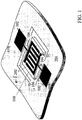
- FIG. 1 shows a mechanical resonating structure 100 according to an embodiment.
- the mechanical resonating structure is connected to pads 102 via anchors 104 according to this embodiment.
- the mechanical resonating structure vibrates in response to a source of excitation (e.g., application of an electrical potential), and is configured (shaped, sized, etc.) to support one or more modes of Lamb waves.
- the mechanical vibration of the mechanical resonating structure may be converted to an electrical output signal which, for example, may be further processed.
- the mechanical resonating structure can generate signals with multiple modes and resonant frequencies, and, as mentioned, is configured to support one or more modes of Lamb waves.
- the mechanical resonating structure can include a resonating structure plate 106 and interdigital transducer (IDT) electrodes 202.
- the mechanical resonating structure includes an active layer 204, as described further below.
- the frequency produced by the mechanical resonating structure may vary depending on the design and application.
- the frequency produced may be between a 1 kHz and 10 GHz.
- the frequencies are in the upper MHz range (e.g., greater than 100 MHz), or at least 1 GHz (e.g., between 1 GHz and 10 GHz).
- the signal may have a frequency of at least 1 MHz (e.g., 13 MHz, 26 MHz) or, in some cases, at least 32 kHz.
- the mechanical resonating structure can be a micromechanical resonator.
- the mechanical resonating structure may have a "large dimension" (i.e., the largest of the length, width, thickness, etc.) of less than 1 mm; in some cases, the large dimension is less than 500 micron, or less than 100 micron, or less than 10 micron.
- the mechanical resonating structure may have any suitable shape.
- the configuration of the mechanical resonating structure can include, for example, any antenna type geometry, as well as beams, cantilevers, free-free bridges, free-clamped bridges, clamped-clamped bridges, discs, rings, prisms, cylinders, tubes, spheres, shells, springs, polygons, diaphragms and tori.
- Any of the mechanical resonating structure elements may be formed either in whole or in part of the same or different geometries.
- several different type geometrical structures may be coupled together to obtain particular resonance mode responses, as described further below. For example, FIG.
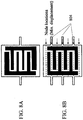
- FIG. 8A shows a mechanical resonating structure design with an IDT electrode configuration that allows reduction in coupling of spurious frequencies and their associated modes.
- additional anchors 804 may be added to support a mechanical resonating structure.
- the anchors can be placed at locations of minimum displacement (of the mechanical resonating structure), so that spurious resonator modes can be suppressed.
- geometrical and structural alterations can be made to improve quality (e.g., Q-factor, noise) of the signal generated by the mechanical resonating structure.
- the mechanical resonating structure may include a plurality of resonating elements. At least some of the resonating elements may be coupled to one another. In some of these embodiments, the resonating elements may have different dimensions.
- the mechanical resonating structure may include at least one major element that has a large dimension that is larger than the large dimension of the minor element.
- the minor elements have at least one smaller dimension (e.g., length, thickness, width) than the major element. Minor elements can have a shorter length than the major element.
- the minor elements may have nanoscale (i.e., less than 1 micron) dimensions. In some embodiments, at least one of the dimensions is less than 1 micron; and, in some embodiments, the large dimension (i.e., the largest of the dimensions) is less than 1 micron.
- Suitable mechanical resonating structures have been described, for example, in International Publication No. WO 2006/083482 , U.S. Patent Application Serial No. 12/181,531, filed July 29, 2008 and published February 4, 2010 as U.S. Patent Application Publication 2010-0026136 , and in U.S. Patent Application Serial No. 12/142,254, filed June 19, 2008 and published October 1, 2009 as U.S. Patent Application Publication 2009-0243 747 . It should be understood that a number of different designs for the mechanical resonating structure are also suitable.
- FIG. 1 also shows one configuration of IDT electrodes and the resonating structure plate according to some embodiments. Other suitable configurations of electrodes can be employed as shall be discussed in further detail below.
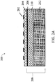
- FIG. 2A illustrates an exemplary lateral view of a mechanical resonating structure.
- the mechanical resonating structure can be built using several components, layers, and materials including IDT electrodes 202, active layer 204, electrode layer(s) 206 and a compensating structure 208.
- the active layer 204 responds to the transduction method used to actuate the mechanical resonating structure (i.e., cause to vibrate) and/or detect motion of the mechanical resonating structure.
- any transduction method may be used including piezoelectric, piezoresistive, electrostatic, electrostrictive, electromotive, magnetostrictive, magnetomotive, thermal, spin-torque effect, and spin-polarized current driven magnetic excitation, amongst others.
- the active layer may have any suitable construction (including composition) which will depend, in part, on the transduction method used for actuation and/or detection.
- the active layer is formed of a piezoelectric material.
- the active layer is formed of a semiconductor material such as silicon. It should be understood that other compositions are also possible.
- the active layer is formed of multiple layers.
- the active layer may comprise multiple layers, one or more of which are functional (e.g., piezoelectric) and one or more of which are not.
- the active layer may be formed of a piezoelectric material.
- suitable materials include aluminum nitride (AlN), zinc oxide (ZnO), cadmium sulfide (CdS), quartz, lead titanate (PbTiO 3 ), lead zirconate titanate (PZT), lithium niobate (LiNbO 3 ) and lithium tantalate (LiTaO 3 ).
- AlN may be preferred.
- Most active layer materials e.g., silicon, piezoelectric materials
- TCS negative temperature coefficient of stiffness
- Stiffness in general, can be associated with a resistance of a material to deform in response to an applied force.
- a mechanical resonating structure comprises a compensation structure.
- the compensation structure is configured to provide a desired stiffness variation of the mechanical resonating structure and/or frequency of operation variation of the mechanical resonating structure over a desired temperature range (e.g., an anticipated operational temperature range of the mechanical resonating structure) for one or more modes of vibration of interest.
- the composition of the active layer of the mechanical resonating structure may be considered in configuring the compensation structure, as the composition of the active layer may impact the stiffness variation of the active layer with temperature, which is to be compensated by the compensation structure in some embodiments.
- the compensation structure may be configured to provide the mechanical resonating structure with a TCF having an absolute value of less than approximately 1 ppm/K over a temperature range of at least 40°C centered around room temperature (25°C) for one or more modes of Lamb waves when the active layer is formed of aluminum nitride.
- TCF having an absolute value of less than approximately 1 ppm/K over a temperature range of at least 40°C centered around room temperature (25°C) for one or more modes of Lamb waves when the active layer is formed of aluminum nitride.
- active layer 204 is formed on compensation structure 208.
- the compensation structure may be formed on the active layer
- compensation structure 208 includes multiple components (e.g., layers).
- characteristics e.g., composition, dimensions, and arrangement within the structure
- characteristics e.g., composition, dimensions, and arrangement within the structure
- the components e.g., layers
- characteristics are selected such that structure 208 provides the desired compensation with respect to the active layer and any additional layers to be compensated, so that the mechanical resonating structure exhibits a desired behavior across a range of temperatures for any modes of vibration of interest.
- the compensating structure includes a first layer 210 and a second layer 212.
- the stiffness of layers 210, 212 may vary differently with temperature.
- layer 210 may have a stiffness that increases with increasing temperature over a temperature range (i.e., a positive TCS).
- Layer 212 may have a stiffness that decreases, or stays relatively constant, with increasing temperature over a temperature range (i.e., a negative TCS).
- the arrangement of the first and second layers e.g., dimensions, location within structure
- the arrangement may be selected so that the resonating structures have a relatively constant stiffness over a temperature range. That is, the TCS may approach or be equal to 0. This may contribute to minimizing the frequency variation over the temperature range (e.g., TCF may approach or be equal to 0).
- the temperature compensation structure may compensate for temperature-induced variations in stiffness of layers other than the active layer (but in addition to the active layer in some embodiments) of the mechanical resonating structure, e.g., one layer of the temperature compensation structure may compensate for temperature-induced stiffness variations of another layer of the temperature compensation structure.
- the compensating structure may include one or more layers in addition to those shown in FIG. 2A . Some of these examples are described further below.
- the additional layer(s) may have the same composition as one of the first or second layers. In other examples, the additional layer(s) may have a different compensation than both the first and second layers.
- the compensation structure may be formed of only a single layer (e.g., first layer 210).
- the active layer may be formed of silicon and the single layer of the compensation structure may be formed of SiO 2 .
- the active layer may be formed of aluminum nitride (AlN) and the single layer of the compensation structure may be formed of silicon dioxide (SiO 2 ). Other choices for the materials may also be used.
- the first layer has characteristics that are selected so that it has a positive TCS (i.e., TCS > 0) over a temperature range.
- the composition of the first layer may be selected to provide a positive TCS. Suitable compositions can include SiO 2 and Al 2 O 3 , amongst others. In some cases, SiO 2 may be preferred.
- the first layer may be composed of a series of ultra-thin layers (e.g., less than 10 nm thick) which are combined to produce an overall layer having a positive TCS.
- the positive TCS may also, or alternatively, be engineered by implanting species (e.g., ions, neutrons) into the first layer.
- a layer exhibiting a positive TCS may be obtained in any of a number of suitable ways, and that the various aspects described herein including one or more layers exhibiting a positive TCS are not limited in the manner in which the positive TCS is obtained.
- first layer 210 has a positive TCS over a temperature range.
- the TCS is positive across the entire operating temperature range of the device.
- the TCS may be positive across the temperature range of between - 55°C and 150°C, or between -40 °C and 85 °C.
- the TCS of first layer 210 may be positive across a portion of the operating range, and negative across other portion(s).
- the TCS of the first layer may be positive across the majority of the temperature range.
- the TCS of the first layer may be positive across a range of at least 200 °C; in some embodiments, at least 100 °C; and, in other embodiments, at least 50 °C.
- second layer 212 may have a different stiffness-temperature dependence than the first layer.
- the second layer may be a support layer that provides robustness to the first layer.
- the second layer may be formed of a material having a lower acoustical loss than the material of the first layer.
- the second layer is formed of a material having a certain crystal structure.
- the second layer may be formed of a single crystal material and/or a material having higher crystal quality than the material of the first layer (e.g., lower defects).
- the robustness and support provided by the second layer is useful, since a structure comprised of a thin SiO 2 layer(s) and the active layer can be fragile and prone to damage if subjected to forceful mechanical movements or vibrations.
- the second layer can also provide improved signal performance (e.g., less noise and better Q-factor).
- Suitable materials for second layer 212 include silicon, diamond, silicon carbide, sapphire, quartz, germanium, aluminum nitride, and gallium arsenide, amongst others. In some embodiments, it is preferable for the second layer to be formed of silicon.
- FIG. 2A includes IDT electrodes 202 and an electrode layer 206 to facilitate transfer of charges and electric potential across a mechanical resonating structure.
- the number of electrodes and placement of electrodes can be important as they can determine the types of acoustic waves and excitation modes generated by the mechanical resonating structure's motion.
- Suitable electrode materials include, but are not limited to, aluminum (Al), molybdenum (Mo), titanium (Ti), chromium (Cr), ruthenium (Ru), gold (Au), platinum (Pt) or AlSiCu.
- Al aluminum
- Mo molybdenum
- Ti titanium
- Cr chromium
- Ru ruthenium
- Au gold
- platinum Pt
- AlSiCu AlSiCu
- any suitable electrode material can be utilized for the electrode layer.
- a thin layer of Ti and/or AlN may be added beneath the electrode to enhance crystal orientation of the active (e.g., piezoelectric) material layer.
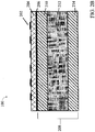
- FIG. 2B illustrates an embodiment in which the compensating structure includes a third layer 214.
- the third layer is formed of a material having a positive TCS. Suitable materials having a positive TCS were described above in connection with first layer 210.
- the third layer comprises the same material as first layer 210. However, in other embodiments, the third layer may comprise a different material than the first layer (and the second layer).
- layers 210 and 214 are formed of SiO 2 layers.
- the second layer 212 is formed of Si. As shown, the second layer is positioned between the first layer and the third layer. Other arrangements are possible.
- the third layer has a similar thickness as the first layer.
- the ratio of the thickness of the third layer to the thickness of the first layer may be between 1:0.25 and 1:4.0, between 1:0.75 and 1:1.25, or about 1:1.
- the listed ratios may be suitable when the third layer is formed of the same composition as the first layer (e.g., when the first and third layers are both formed of SiO 2 , or any other suitable material (e.g., any other suitable positive TCS material)).
- the three-layer compensation structure configuration illustrated in FIG. 2B may provide enhanced performance as compared to a two-layer compensating structure.
- such a configuration can reduce the tendency of the resonating structure to bend out of plane by balancing residual stress in the structure. This can provide a high Q, low noise signal.
- a split-layer compensation structure similar to that illustrated in FIG. 2B may facilitate fabrication of the structure.
- the layers 210 and 214 may be formed of the same material (e.g., SiO 2 ). Rather than forming a single layer of the material having a thickness approximately equal to the combined thickness of layers 210 and 214, the configuration of FIG.
- 2B may be used in which separate layers 210 and 214 are formed. In this manner, fabrication defects associated with forming thick material layers (e.g., cracking, bending, warping, etc.) may be minimized or avoided, as may be out-of-plane deformation of the mechanical resonating structure.
- fabrication defects associated with forming thick material layers e.g., cracking, bending, warping, etc.
- the compensation structure may have a variety of different configurations in addition to those shown in FIGS. 2A and 2B .
- the compensation structure may include more than three layers.
- the compensation structure may include at least one additional layer having a similar function as second layer 212 described above.
- the additional one or more layer(s) may be formed of a material having a lower acoustical loss than the material of the first layer including those noted above.
- the additional one or more layer(s) is formed of silicon.
- the compensation structures can be designed to provide the mechanical resonating structure with a desired frequency variation with temperature (e.g., TCF) for one or more modes of interest.
- TCF desired frequency variation with temperature
- the TCF may be desirable for the TCF to approximate or be equal to zero over a range of temperatures for one or more modes of Lamb waves, or for any other modes of interest. That is, in these cases, the compensating structure can enable the mechanical resonating structure to operate with little or no variation in frequency over a range of temperatures.
- the TCF may be non-zero at least over certain temperature ranges.
- the frequency of the mechanical resonating structure may vary a desired amount with temperature.
- the compensation structure is designed to achieve the desired amount of variation.
- the mechanical resonating structure has an absolute value of a TCF of less than 10 ppm/K over a range of temperatures.
- the absolute value of the TCF may be less than 10 over an anticipated operating range of the mechanical resonating structure (e.g., from -40°C to 85°C).
- the absolute value of the TCF is less than 6 ppm/K over a range of temperatures, for example from -40°C to 85°C.
- the absolute value of the TCF over the range of temperatures is less than 5 ppm/K, or less than 3 ppm/K, less than 2 ppm/K or less than 1 ppm/K.
- the TCF may approximately equal 0 (which includes exactly equaling zero) over a range of at least 5°C or at least 10°C within the range from -40°C to 85°C, as a non-limiting example. Other values are also possible.
- the absolute value of the TCF may be less than 4 ppm/K, less than 1 ppm/K, less than 0.5 ppm/k, or approximately zero, over a range of temperature spanning at least 40°C (e.g., a range of temperatures spanning at least 40°C and centered approximately at room temperature, 25°C).
- the range of temperatures over which the desired TCF is achieved may depend on the application. In some cases, the temperature range may be broad. For example, the temperature range may be between -55°C and 150°C; or, -40°C to 85°C. The range may span at least 200°C, at least 100°C, at least 75°C, at least 50°C, or at least 40°C. In other embodiments, the range of temperature over which the desired TCF is achieved may be more narrow. For example, the temperature range may be less than 50°C, less than 25°C, or less than 10°C. In general, the above-noted ranges of temperatures can be centered around any desired temperature. For example, they may be centered around room temperature (i.e., 25°C), an elevated temperature such as 100°C, or otherwise.
- the compensation structure may be designed to result in a mechanical resonating structure with a desired TCF by selecting appropriate characteristics for the compensation structure.
- the characteristics may include the composition, dimensions, and arrangement of layers within the structure.
- the thickness of the active layer e.g., layer 204
- the total thickness of the positive TCS material layer(s) e.g., layer 210 in FIG. 2A and layers 210, 214 in FIG. 2B
- the ratio of the thickness of the active layer to the total thickness of the positive TCS material layer(s) may be between 1:1 and 1:500, or between 1:1 and 1:200 in some non-limiting embodiments. In some embodiments, the ratio may be between 1:1 and 1:10, or between 1:4 and 1:8, or between 1:5 and 1:7 (e.g., about 1:6).
- the active layer may be formed of aluminum nitride and the positive TCS material of the compensation structure may be formed of silicon dioxide, although other materials may be used for the active layer and positive TCS material layer, as those listed are merely examples.
- the total thickness of the positive TCS material layer(s) includes the sum of the thickness of all such layers.
- the total thickness of the positive TCS material layer(s) is the thickness of that single layer.
- the above-noted ratios for example, may be suitable when the positive TCS material in the layer(s) is SiO 2 and the active material is a piezoelectric material such as AlN. Other ratios may be suitable depending on the materials used.
- the thickness of the positive TCS material layer(s) and the thickness of the layer(s) having a lower acoustic loss than the positive TCS material layer(s) are selected to provide a desired ratio.
- the ratio of the total thickness of the positive TCS material layer(s) e.g., the combined thickness of multiple positive TCS layers in those embodiments in which the compensation structure includes multiple positive TCS layers
- the layer(s) having a lower acoustic loss than the positive TCS material layer(s) may be between 1:0.1 and 1:10, 1:0.5 and 1:3, between 1:0.75 and 1:1.25, or between 1:1 and 1:2.
- the above-noted ratios may be suitable when, for example, the positive TCS material in the layer(s) is SiO 2 and the layer(s) having a lower acoustic loss than the positive TCS material layer(s) is/are formed of Si. These ratios may be suitable when the active material is a piezoelectric material such as AlN.
- the ratio of the thickness of the active layer(s) of the mechanical resonating structure compared to the thickness of any layers of the temperature compensation structure having lower acoustic loss may be designed to fall within certain ranges.
- the ratio of the thickness of the active layer to the total thickness of one or more layers of the temperature compensation structure having lower acoustic loss than the positive TCS layer(s) may be between 1:0.1 and 1:500, and in some embodiments may be between 1:0.5 and 1:20.
- Such ratios may be suitable when the active layer comprises, for example, AlN, and the layer of lower acoustic loss material comprises, for example, silicon. Other materials and other ratios may be used, however, as those listed are not limiting.
- FIGS. 2-3D and FIGS. 3H-3J illustrate some embodiments of the invention.
- Other configurations of a mechanical resonating structure can be utilized.
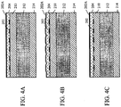
- FIGS. 4A-4C illustrate 3 different configurations of a mechanical resonating structure.
- a top electrode 202A can be placed on top of active layer 204 (e.g., AlN).
- the compensating structure can be situated below the active layer with IDT electrodes 202 located at an interface of the compensating structure and the active layer.
- the compensating structure can be a Si layer 212 placed between two SiO 2 layers 210, 214 of equal thickness.
- FIG. 4A illustrates a configuration in which the IDT electrodes are not placed on the top surface of the mechanical resonating structure and in which the active layer is planarized.
- FIG. 4B illustrates a similar structure to FIG. 4A with a difference that the top electrode and active layer are not planarized.
- FIG. 4C also illustrates a configuration similar to FIG. 4A ; however, in contrast to FIG. 4A , the IDT electrodes in FIG. 4C are embedded in a first SiO 2 layer of the compensating structure.
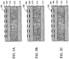
- FIGS. 5A-5C illustrate another set of embodiments in which top 202 and bottom 504 IDT electrodes are used in a mechanical resonating structure.
- bottom electrodes are placed within the active layer 204 at an interface with the compensating structure as in FIGS. 4A and 4B .
- an additional set of top IDT electrodes are deposited on the top surface of the active layer.
- FIG. 5B illustrates a non-planarized structure as compared to the planarized structured in FIG. 5A.
- FIG. 5C shows the bottom IDT electrodes being situated within the first SiO 2 layer 210 of the compensating structure.
- various configurations of a mechanical resonating structure with zero TCS can be designed and utilized.
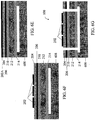
- FIGS. 6A-6G and FIGS. 7A-7F illustrate two possible processes used to fabricate a mechanical resonating structure according to embodiments of the invention. It should be understood that other fabrication techniques are also possible including techniques in which the specific process steps are re-arranged in a different order.
- FIGS. 6A-6G A first fabrication process is shown in FIGS. 6A-6G .
- Structure 600A including a handle layer 602, a first layer 210 with a stiffness that increases with temperature (e.g., SiO 2 or any suitable oxide layer), and a second layer 212 with a stiffness that decreases with temperature (e.g., Si), can be used to commence the fabrication process.
- the first layer can be buried between the handle layer and the second layer.
- the handle and second layers can be Si layers.
- thermal oxide layers 604, 214 can be formed on a top surface of the handle layer and a bottom surface of the second layer using a suitable thermal oxidation procedure.
- the added thermal oxide layers can be similar to a thickness of the buried first layer 210.
- a wafer 608 with cavity 606 can be bonded to structure 600A, as illustrated in FIG. 6C . Bonding the wafer to structure 600A yields a modified structure 600B with a pre-defined cavity.
- the handle layer 602 and oxide layer 604 can be removed and a planarized top first layer may be formed using any suitable planarization procedure (e.g., chemical mechanical planarization (CMP).
- CMP chemical mechanical planarization
- a bottom electrode layer 206, an active layer 204 and a top electrode layer 202A can be deposited on the top, planarized surface of first layer 210 ( FIG. 6E ).
- Suitable deposition techniques include, for example, chemical vapor deposition (CVD) and physical vapor deposition (PVD). In general, any suitable deposition technique can be used.
- Portions of the top electrode layer can then be selectively removed using any suitable photolithography process. The selective removal can result in formation of IDT electrodes 202 as shown in FIG. 6F .
- the active layer, the electrode layer, the first layer, the second layer and the oxide layer can be etched until the cavity is reached to yield a suspended resonating structure 100 as shown in FIG. 6G .
- Anchors and other components e.g., pads, vias compensating the suspended resonating structure are not shown in FIG. 6G .
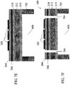
- FIGS. 7A-7F illustrate another process that can be used to fabricate a mechanical resonating structure according to some embodiments.
- a structure 700A with a handle layer 702, an oxide layer 214 and a second layer 212 with a stiffness that decreases with temperature (e.g., Si) can be used to commence the fabrication process.
- a first layer 210 with a stiffness that increases with temperature (e.g., SiO 2 or any suitable oxide layer), a bottom electrode layer 206, a active layer 204 and a top electrode layer 202A can be deposited on the second layer as shown in FIGS. 7B and 7C .
- the first layer 210 can have the same thickness as oxide layer 214. Examples of suitable deposition techniques have been described above.
- the top electrode layer is partially removed to form IDT electrodes 202 as described above and shown in FIG. 7D .
- the handle layer is selectively etched to the bottom surface of oxide layer 214 to form a cavity 606 as shown in FIG. 7E . Further etching 704 of the active layer, the bottom electrode layer, the second layer, the first layer and the oxide layer can result in a suspended resonating structure 100 illustrated in FIG. 7F .
- a mechanical resonating structure can be integrated in tunable meters, mass sensors, gyros, accelerometers, switches, and electromagnetic fuel sensors.
- the mechanical resonating structure can be integrated in a timing oscillator.
- Timing oscillators can be used in several devices including digital clocks, radios, computers, oscilloscopes, signal generators, and cell phones. Timing oscillators can precisely generate clock signals, for example, as a reference frequency to help synchronize other signals that are received, processed, or transmitted by a device in which the timing oscillator is integrated.
- a mechanical resonating structure can also be coupled to additional circuitry.
- additional circuitry may include filters, mixers, dividers, amplifiers or other application specific components and devices.
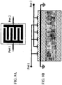
- the mechanical resonating structure can be used as a multiple port device.
- the bottom electrode can be grounded, while the IDT electrodes are coupled to two ports, namely Port 1 and Port 2.
- the bottom electrode could be a floating node.
- a dual mechanical resonating structure structure can be utilized to create a four-port mechanical resonating structure device. In the dual mechanical resonating structure configuration, two mechanical resonating structures can be implemented on the same resonating structure plate and the ports can be connected to the desired inputs and outputs.
- layers 210, 214 are formed of SiO 2 and layer 212 is formed of Si.
- FIG. 3E is an indicator of how the TCF varies as a function of temperature. Specifically, FIG. 3E shows a graph of the normalized frequency variation ( ⁇ f/f) versus temperature. The TCF corresponds to the slope of this curve. As noted above, the active layer can have a negative TCF, and SiO 2 can have a positive TCF for a specified range of temperatures.
- FIG. 3A shows an example of a mechanical resonating structure with an active layer (e.g., AlN), a bottom electrode, a Si layer 212 and no SiO 2 layers.
- This structure has a negative TCF of approximately -30 ppm/K (illustrated by line A in FIG. 3E).
- FIG. 3B shows an example of a mechanical resonating structure with a Si layer placed between two SiO 2 laye as discussed above.
- the SiO 2 layers have a relatively small thickness compared to the Si layer and to corresponding SiO 2 layers in FIGS. 3B and 3C .
- the low thickness can result in a TCF that is still negative but greater (i.e., less negative) than the TCF of the mechanical resonating structure in FIG. 3A .
- the structure shown in FIG. 3C is similar to the mechanical resonating structure in FIG. 3B ; however, in FIG. 3C , both SiO 2 layers have greater thicknesses.
- the corresponding line, C, in FIG. 3E indicates an almost zero TCF for the mechanical resonating structure in FIG. 3C .
- the thickness of the SiO 2 layers is further increased, as shown in FIG. 3D , then the TCF of the mechanical resonating structure becomes non-zero and positive, as shown by D in FIG. 3E . Accordingly, in these embodiments, the thinner the thickness of the SiO 2 layers, the more negative the TCF of the mechanical resonating structure.
- FIG. 3E illustrates an example of how the normalized frequency variation ( ⁇ f/f) over temperature can be 'leveled' and, therefore, the TCF approaches zero over a range of temperatures by selecting appropriate thicknesses for layers of a mechanical resonating structure device
- it may be more challenging to achieve a flat response over a broad range of temperatures e.g., -40°C to 85°C
- the mechanical resonating structure may be designed and/or tuned to provide zero TCF properties around the operating temperature (e.g., room temperature) or any other desired/pre-determined temperature of the mechanical resonating structure. For example, as illustrated in FIG.
- a non-linear curve C can have a zero TCF at room temperature (i.e., 25°C) if suitable thicknesses are chosen for the mechanical resonating structure layers. If, for example, a slightly thicker SiO 2 layer is used, a zero TCF can be achieved at a temperature greater than room temperature, as indicated by curve C + ; however, if a slightly thinner SiO 2 layer is used, a zero TCF can be achieved at a temperature lower than room temperature, as indicated by curve C - .
- the thicknesses of the mechanical resonating structure layers may not only determine where a zero TCF is achieved in a broad range of temperatures, but may also help reduce the higher-order nature of the mechanical resonating structure layers' non-linear TCF properties.
- FIG. 3G shows the parabolic TCF profile of three mechanical resonating structures A, B and C illustrated in FIGS. 3H-3J .
- Structure C has a smaller Si / SiO 2 layer thickness than structure B, which has a smaller Si / SiO 2 layer thickness than structure A. Due to differences in a ratio of the thickness of the active material to the thickness of the Si layer and/or the SiO 2 layers, the parabolic profile of all three structures can be different despite having a zero TCF at room temperature.
Landscapes
- Physics & Mathematics (AREA)
- Acoustics & Sound (AREA)
- Piezo-Electric Or Mechanical Vibrators, Or Delay Or Filter Circuits (AREA)
- Surface Acoustic Wave Elements And Circuit Networks Thereof (AREA)
- Micromachines (AREA)
Claims (11)
- Vorrichtung, umfassend:eine mechanische Resonanzstruktur (100), welche konfiguriert ist, um Lamb-Wellen zu tragen, und welche aufweist:dadurch gekennzeichnet, dasseine aktive Schicht (204); undeine Kompensationsstruktur (208), welche konfiguriert ist, um eine gewünschte Steifigkeitsvariation der mechanischen Resonanzstruktur und/oder Betriebsfrequenzvariation der mechanischen Resonanzstruktur über einen gewünschten Temperaturbereich für eine oder mehrere Vibrationsmoden bereitzustellen, wobei die Kompensationsstruktur mit der aktiven Schicht gekoppelt ist und umfasst:eine erste Schicht (210) mit einer Steifigkeit, welche mit ansteigender Temperatur über zumindest den gewünschten Temperaturbereich ansteigt,
die Kompensationsstruktur (208) ferner umfasst:eine dritte Schicht (214) mit einer Steifigkeit, welche mit ansteigender Temperatur über zumindest den gewünschten Temperaturbereich ansteigt, undeine zweite Schicht (212) zwischen der ersten Schicht (210) und der dritten Schicht (214), wobei die zweite Schicht (212) sich von der ersten und dritten Schicht (210, 214) unterscheidet. - Vorrichtung gemäß Anspruch 1, wobei die aktive Schicht (204) ein piezoelektrisches Material umfasst.
- Vorrichtung gemäß einem der vorhergehenden Ansprüche, wobei die aktive Schicht (204) Aluminiumnitrid umfasst.
- Vorrichtung gemäß einem der vorhergehenden Ansprüche, wobei die erste Schicht (210) und die dritte Schicht (214) der Kompensationsstruktur (208) aus einem ersten Material ausgebildet sind.
- Vorrichtung gemäß einem der vorhergehenden Ansprüche, wobei die erste Schicht (210) und die dritte Schicht (214) der Kompensationsstruktur (208) ungefähr dieselbe Dicke wie die jeweils andere aufweisen.
- Vorrichtung gemäß einem der vorhergehenden Ansprüche, wobei die erste Schicht (210) der Kompensationsstruktur (208) aus einem ersten Material ausgebildet ist und wobei die zweite Schicht (212) aus einem zweiten, von dem ersten Material verschiedenen Material ausgebildet ist,
wobei vorzugsweise das erste Material Silikondioxid ist und das zweite Material Silikon ist, und wobei vorzugsweise ein Verhältnis einer gesamten Dicke von einer oder zwei Schichten der mechanischen Resonanzstruktur, welche das erste Material umfasst, zu einer gesamten Dicke von einer oder zwei Schichten der mechanischen Resonanzstruktur, welche das zweite Material umfasst, zwischen 1:0,75 und 1:2 ist. - Vorrichtung gemäß Anspruch 6, wobei ein Verhältnis einer gesamten Dicke von einer oder zwei Schichten der mechanischen Resonanzstruktur, welche das erste Material umfasst, zu einer Dicke der aktiven Schicht (204) zwischen 1:0,1 und 1:1,25 ist, vorzugsweise zwischen 1:0,2 und 1:0,75.
- Vorrichtung gemäß einem der vorhergehenden Ansprüche, wobei die erste Schicht (210) aus Silikondioxid ausgebildet ist.
- Vorrichtung gemäß einem der vorhergehenden Ansprüche, wobei die zweite Schicht (212) aus einem Material ausgebildet ist, welches aus der Gruppe ausgewählt ist, welche aus Silikon, Siliciumcarbid, Saphir, Quartz, Germanium, Galliumarsenid, Aluminiumnitrid und Diamant besteht, wobei die zweite Schicht vorzugsweise aus Silikon ausgebildet ist.
- Vorrichtung gemäß einem der vorhergehenden Ansprüche, wobei die aktive Schicht aus mehreren Schichten ausgebildet ist, wobei eine oder mehrere davon aus einem piezoelektrischen Material ausgebildet sind und wobei eine oder mehrere davon aus Silikon ausgebildet sind.
- Vorrichtung gemäß einem der vorhergehenden Ansprüche, wobei die aktive Schicht (204) auf der Kompensationsstruktur (208) ausgebildet ist.
Applications Claiming Priority (2)
| Application Number | Priority Date | Filing Date | Title |
|---|---|---|---|
| US13817108P | 2008-12-17 | 2008-12-17 | |
| PCT/US2009/006590 WO2010077313A1 (en) | 2008-12-17 | 2009-12-16 | Mechanical resonating structures including a temperature compensation structure |
Publications (3)
| Publication Number | Publication Date |
|---|---|
| EP2377176A1 EP2377176A1 (de) | 2011-10-19 |
| EP2377176A4 EP2377176A4 (de) | 2012-08-22 |
| EP2377176B1 true EP2377176B1 (de) | 2016-12-14 |
Family
ID=42310056
Family Applications (1)
| Application Number | Title | Priority Date | Filing Date |
|---|---|---|---|
| EP09836502.6A Active EP2377176B1 (de) | 2008-12-17 | 2009-12-16 | Mechanische resonierende strukturen mit einer temperaturkompensationsstruktur |
Country Status (4)
| Country | Link |
|---|---|
| US (5) | US8058769B2 (de) |
| EP (1) | EP2377176B1 (de) |
| JP (2) | JP5848131B2 (de) |
| WO (1) | WO2010077313A1 (de) |
Families Citing this family (71)
| Publication number | Priority date | Publication date | Assignee | Title |
|---|---|---|---|---|
| US8410868B2 (en) | 2009-06-04 | 2013-04-02 | Sand 9, Inc. | Methods and apparatus for temperature control of devices and mechanical resonating structures |
| US8476809B2 (en) | 2008-04-29 | 2013-07-02 | Sand 9, Inc. | Microelectromechanical systems (MEMS) resonators and related apparatus and methods |
| US8686614B2 (en) * | 2008-12-17 | 2014-04-01 | Sand 9, Inc. | Multi-port mechanical resonating devices and related methods |
| US8689426B2 (en) | 2008-12-17 | 2014-04-08 | Sand 9, Inc. | Method of manufacturing a resonating structure |
| EP2377176B1 (de) * | 2008-12-17 | 2016-12-14 | Analog Devices, Inc. | Mechanische resonierende strukturen mit einer temperaturkompensationsstruktur |
| US8040207B2 (en) * | 2009-01-15 | 2011-10-18 | Infineon Technologies Ag | MEMS resonator devices with a plurality of mass elements formed thereon |
| WO2010110918A1 (en) * | 2009-03-26 | 2010-09-30 | Sand9, Inc. | Mechanical resonating structures and methods |
| US9048811B2 (en) | 2009-03-31 | 2015-06-02 | Sand 9, Inc. | Integration of piezoelectric materials with substrates |
| US8174170B1 (en) | 2009-05-13 | 2012-05-08 | Sand 9, Inc. | Methods and apparatus for mechanical resonating structures |
| US8664836B1 (en) * | 2009-09-18 | 2014-03-04 | Sand 9, Inc. | Passivated micromechanical resonators and related methods |
| US8228127B2 (en) | 2009-12-23 | 2012-07-24 | Sand 9, Inc. | Oscillators having arbitrary frequencies and related systems and methods |
| US8661899B2 (en) * | 2010-03-01 | 2014-03-04 | Sand9, Inc. | Microelectromechanical gyroscopes and related apparatus and methods |
| WO2011133682A1 (en) | 2010-04-20 | 2011-10-27 | Guiti Zolfagharkhani | Microelectromechanical gyroscopes and related apparatus and methods |
| US8916942B2 (en) * | 2010-05-13 | 2014-12-23 | Valtion Teknillinen Tutkimuskeskus | Microelectromechanical resonator and a method for producing the same |
| WO2012009429A1 (en) | 2010-07-13 | 2012-01-19 | Sand9, Inc. | Methods and apparatus for calibration and temperature compensation of oscillators having mechanical resonators |
| US9075077B2 (en) | 2010-09-20 | 2015-07-07 | Analog Devices, Inc. | Resonant sensing using extensional modes of a plate |
| EP2624451B1 (de) * | 2010-09-28 | 2017-06-07 | Murata Manufacturing Co., Ltd. | Verfahren zur herstellung einer piezoelektrischen vorrichtung |
| US9583354B2 (en) | 2011-03-30 | 2017-02-28 | The Aerospace Corporation | Systems and methods for depositing materials on either side of a freestanding film using laser-assisted chemical vapor deposition (LA-CVD), and structures formed using same |
| US9679779B2 (en) * | 2011-03-30 | 2017-06-13 | The Aerospace Corporation | Systems and methods for depositing materials on either side of a freestanding film using selective thermally-assisted chemical vapor deposition (STA-CVD), and structures formed using same |
| US8704428B2 (en) | 2011-04-20 | 2014-04-22 | Qualcomm Mems Technologies, Inc. | Widening resonator bandwidth using mechanical loading |
| US20120293520A1 (en) * | 2011-05-19 | 2012-11-22 | Qualcomm Mems Technologies, Inc. | Piezoelectric resonators with configurations having no ground connections to enhance electromechanical coupling |
| US9013088B1 (en) * | 2011-07-07 | 2015-04-21 | Sand 9, Inc. | Field effect control of a microelectromechanical (MEMS) resonator |
| US9590587B1 (en) | 2011-07-07 | 2017-03-07 | Analog Devices, Inc. | Compensation of second order temperature dependence of mechanical resonator frequency |
| KR101853740B1 (ko) | 2011-07-27 | 2018-06-14 | 삼성전자주식회사 | 체적 음향 공진기 및 체적 음향 공진기를 이용한 듀플렉서 |
| JP5815329B2 (ja) * | 2011-08-22 | 2015-11-17 | 太陽誘電株式会社 | 弾性波デバイス |
| US9383208B2 (en) | 2011-10-13 | 2016-07-05 | Analog Devices, Inc. | Electromechanical magnetometer and applications thereof |
| US9000854B1 (en) | 2011-10-28 | 2015-04-07 | Sand 9, Inc. | Timing oscillator having a non-linear MEMS resonator and related methods |
| JP5946385B2 (ja) * | 2011-12-05 | 2016-07-06 | 日本電波工業株式会社 | 共振子 |
| GB201121660D0 (en) * | 2011-12-15 | 2012-01-25 | Cambridge Entpr Ltd | Measurement method using a sensor, sensor system and sensor |
| US9214623B1 (en) | 2012-01-18 | 2015-12-15 | Analog Devices, Inc. | Doped piezoelectric resonator |
| US8896188B2 (en) | 2012-04-11 | 2014-11-25 | Sand 9, Inc. | Resonator electrodes and related methods and apparatus |
| US9537466B1 (en) | 2012-05-02 | 2017-01-03 | Analog Devices, Inc. | Microelectromechanical system resonators and related methods and apparatus |
| US9299910B1 (en) | 2012-05-17 | 2016-03-29 | Analog Devices, Inc. | Resonator anchors and related apparatus and methods |
| US9000848B2 (en) | 2012-07-16 | 2015-04-07 | Sand 9, Inc. | Noise reduction in MEMS oscillators and related apparatus and methods |
| US8990655B2 (en) | 2012-09-28 | 2015-03-24 | Intel Corporation | Techniques associated with error correction for encoded data |
| WO2014090302A1 (en) * | 2012-12-12 | 2014-06-19 | Epcos Ag | Electroacoustic component |
| US9246516B2 (en) | 2012-12-20 | 2016-01-26 | Intel Corporation | Techniques for error correction of encoded data |
| US9954513B1 (en) | 2012-12-21 | 2018-04-24 | Analog Devices, Inc. | Methods and apparatus for anchoring resonators |
| US9634227B1 (en) | 2013-03-06 | 2017-04-25 | Analog Devices, Inc. | Suppression of spurious modes of vibration for resonators and related apparatus and methods |
| KR20160001052A (ko) * | 2014-06-26 | 2016-01-06 | 삼성전기주식회사 | 피에조 구동 장치 및 방법 |
| US10348269B2 (en) | 2014-12-17 | 2019-07-09 | Qorvo Us, Inc. | Multi-frequency guided wave devices and fabrication methods |
| FR3046090B1 (fr) * | 2015-12-28 | 2021-06-25 | Frecnsys | Perfectionnement aux transducteurs a ondes de volume guidees en surface |
| FI127787B (en) | 2016-07-01 | 2019-02-28 | Teknologian Tutkimuskeskus Vtt Oy | Micromechanical resonator |
| US10800649B2 (en) | 2016-11-28 | 2020-10-13 | Analog Devices International Unlimited Company | Planar processing of suspended microelectromechanical systems (MEMS) devices |
| JP6822118B2 (ja) * | 2016-12-19 | 2021-01-27 | セイコーエプソン株式会社 | 振動子、発振器、電子機器、および移動体 |
| US10547286B2 (en) * | 2017-02-03 | 2020-01-28 | Samsung Electro-Mechanics Co., Ltd. | Filter and front end module including the same |
| US10498001B2 (en) | 2017-08-21 | 2019-12-03 | Texas Instruments Incorporated | Launch structures for a hermetically sealed cavity |
| US10775422B2 (en) | 2017-09-05 | 2020-09-15 | Texas Instruments Incorporated | Molecular spectroscopy cell with resonant cavity |
| US10589986B2 (en) | 2017-09-06 | 2020-03-17 | Texas Instruments Incorporated | Packaging a sealed cavity in an electronic device |
| US10444102B2 (en) | 2017-09-07 | 2019-10-15 | Texas Instruments Incorporated | Pressure measurement based on electromagnetic signal output of a cavity |
| US10424523B2 (en) | 2017-09-07 | 2019-09-24 | Texas Instruments Incorporated | Hermetically sealed molecular spectroscopy cell with buried ground plane |
| US10551265B2 (en) | 2017-09-07 | 2020-02-04 | Texas Instruments Incorporated | Pressure sensing using quantum molecular rotational state transitions |
| US10549986B2 (en) | 2017-09-07 | 2020-02-04 | Texas Instruments Incorporated | Hermetically sealed molecular spectroscopy cell |
| US10131115B1 (en) * | 2017-09-07 | 2018-11-20 | Texas Instruments Incorporated | Hermetically sealed molecular spectroscopy cell with dual wafer bonding |
| US10544039B2 (en) | 2017-09-08 | 2020-01-28 | Texas Instruments Incorporated | Methods for depositing a measured amount of a species in a sealed cavity |
| US11050405B2 (en) * | 2018-01-16 | 2021-06-29 | Government Of The United States Of America, As Represented By The Secretary Of Commerce | Micromechanical vibrasolator |
| WO2019169025A1 (en) * | 2018-03-02 | 2019-09-06 | Skyworks Solutions, Inc. | Lamb wave loop circuit for acoustic wave filter |
| WO2020074075A1 (en) * | 2018-10-10 | 2020-04-16 | Joanneum Research Forschungsgesellschaft Mbh | Piezoelectric sensor |
| US10843920B2 (en) | 2019-03-08 | 2020-11-24 | Analog Devices International Unlimited Company | Suspended microelectromechanical system (MEMS) devices |
| US20210184653A1 (en) * | 2019-12-12 | 2021-06-17 | University Of Florida Research Foundation, Incorporated | Acoustically coupled radio frequency (rf) filter |
| GB2598665B (en) * | 2020-09-04 | 2025-07-23 | Skyworks Solutions Inc | Multi-layer piezoelectric substrate with controllable delta temperature coefficient of frequency |
| AT524289B1 (de) * | 2020-10-12 | 2025-04-15 | Pacemaker Tech Gmbh | Verfahren zur Kraft- bzw. Druckmessung, insbesondere für eine Ganganalyse, mit einem piezoelektrischen Sensor sowie piezoelektrischer Sensor hierzu |
| FI129591B (en) * | 2020-11-06 | 2022-05-13 | Kyocera Tikitin Oy | Mems resonator with high quality factor and its use |
| EP4270505A4 (de) * | 2020-12-28 | 2024-12-04 | I-PEX Piezo Solutions Inc. | Filmstruktur und elektronische vorrichtung |
| US12696688B2 (en) * | 2021-01-29 | 2026-07-28 | Skyworks Solutions, Inc. | Piston mode generation in thin plate lamb wave device |
| JP7710890B2 (ja) * | 2021-05-17 | 2025-07-22 | 太陽誘電株式会社 | 弾性波デバイス、ウエハ、フィルタおよびマルチプレクサ |
| US12415718B2 (en) * | 2021-06-25 | 2025-09-16 | Taiwan Semiconductor Manufacturing Company, Ltd. | Impact-resistant micromechanical arms |
| US12686611B2 (en) * | 2022-06-30 | 2026-07-21 | Texas Instruments Incorporated | Micro-acoustic resonator springy anchor based on offset acoustic reflector trenches |
| US12665569B2 (en) | 2022-09-09 | 2026-06-23 | Skyworks Solutions, Inc. | Multilayer piezoelectric substrate filters with consistent band balance |
| DE102023107892A1 (de) * | 2023-03-28 | 2024-10-02 | Endress+Hauser SE+Co. KG | Anordnung zur Temperaturkompensation einer Komponente eines Bauteils |
| CN120629637B (zh) * | 2025-06-30 | 2026-06-05 | 西安交通大学 | 一种低应力mems谐振式加速度计 |
Family Cites Families (77)
| Publication number | Priority date | Publication date | Assignee | Title |
|---|---|---|---|---|
| US3916348A (en) | 1975-01-31 | 1975-10-28 | Rca Corp | Temperature-compensated surface-propagated wave energy device |
| US4454440A (en) | 1978-12-22 | 1984-06-12 | United Technologies Corporation | Surface acoustic wave (SAW) pressure sensor structure |
| US4384409A (en) | 1980-10-18 | 1983-05-24 | The Bendix Corporation | Surface acoustic wave gyroscope |
| JPS57145419A (en) * | 1981-03-05 | 1982-09-08 | Clarion Co Ltd | Surface acoustic wave element |
| JPS5964908A (ja) * | 1982-10-05 | 1984-04-13 | Nobuo Mikoshiba | 弾性表面波素子 |
| JPS6194409A (ja) | 1984-10-15 | 1986-05-13 | Clarion Co Ltd | 弾性表面波素子の素子分離構造 |
| WO1989008336A1 (en) | 1988-02-29 | 1989-09-08 | The Regents Of The University Of California | Plate-mode ultrasonic sensor |
| JPH027525A (ja) | 1988-06-27 | 1990-01-11 | Seiko Epson Corp | 半導体装置の製造方法 |
| TW438155U (en) * | 1995-07-27 | 2001-05-28 | Daishinku Corp | Multi-mode piezoelectric filter |
| WO1998001948A1 (en) | 1996-07-03 | 1998-01-15 | International Business Machines Corporation | Mechanical signal processor comprising means for loss compensation |
| IL129573A0 (en) | 1996-11-15 | 2000-02-29 | Baxter Int | Conditioning for allogeneic stem cell transplantation |
| JPH10209801A (ja) * | 1997-01-28 | 1998-08-07 | Murata Mfg Co Ltd | 表面波装置 |
| US5914553A (en) * | 1997-06-16 | 1999-06-22 | Cornell Research Foundation, Inc. | Multistable tunable micromechanical resonators |
| US6124765A (en) * | 1997-10-24 | 2000-09-26 | Stmicroelectronics, Inc. | Integrated released beam oscillator and associated methods |
| JPH11239037A (ja) | 1998-02-20 | 1999-08-31 | Nec Corp | 弾性表面波装置 |
| US6516665B1 (en) | 1999-06-17 | 2003-02-11 | The Penn State Research Foundation | Micro-electro-mechanical gyroscope |
| EP1154570B1 (de) | 1999-12-17 | 2016-03-09 | Tohoku Techno Arch Co., Ltd. | Akustische oberflächenwellenanordnung |
| DE19961857A1 (de) | 1999-12-22 | 2001-06-28 | Endress Hauser Gmbh Co | Verfahren zur Erregung von Lambwellen in einer Platte, insbesondere in einer Behälterwand, und Vorrichtung zur Durchführung des Verfahrens und zum Empfang der erregten Lambwellen |
| US6848295B2 (en) | 2002-04-17 | 2005-02-01 | Wayne State University | Acoustic wave sensor apparatus, method and system using wide bandgap materials |
| US6739190B2 (en) * | 2000-08-24 | 2004-05-25 | The Regents Of The University Of Michigan | Micromechanical resonator device |
| JP3682224B2 (ja) * | 2000-12-19 | 2005-08-10 | 日本電波工業株式会社 | 4ポール・モノリシック・フィルタ |
| US6747389B2 (en) * | 2001-06-11 | 2004-06-08 | Intel Corporation | Apparatus for adjusting the resonance frequency of a microelectromechanical (MEMS) resonator using tensile/compressive strain and applications therefor |
| WO2003055063A1 (en) * | 2001-12-06 | 2003-07-03 | University Of Pittsburgh | Tunable piezoelectric micro-mechanical resonator |
| US7943412B2 (en) * | 2001-12-10 | 2011-05-17 | International Business Machines Corporation | Low temperature Bi-CMOS compatible process for MEMS RF resonators and filters |
| US7276994B2 (en) | 2002-05-23 | 2007-10-02 | Murata Manufacturing Co., Ltd. | Piezoelectric thin-film resonator, piezoelectric filter, and electronic component including the piezoelectric filter |
| US6828713B2 (en) * | 2002-07-30 | 2004-12-07 | Agilent Technologies, Inc | Resonator with seed layer |
| US6909221B2 (en) * | 2002-08-01 | 2005-06-21 | Georgia Tech Research Corporation | Piezoelectric on semiconductor-on-insulator microelectromechanical resonators |
| WO2004059836A2 (en) * | 2002-08-06 | 2004-07-15 | Charles Stark Draper Laboratory Inc. | Piezoelectric mems resonator |
| US7023065B2 (en) | 2002-08-07 | 2006-04-04 | Georgia Tech Research Corporation | Capacitive resonators and methods of fabrication |
| US6987432B2 (en) * | 2003-04-16 | 2006-01-17 | Robert Bosch Gmbh | Temperature compensation for silicon MEMS resonator |
| KR20060026905A (ko) * | 2003-07-02 | 2006-03-24 | 소니 가부시끼 가이샤 | Mems형 진동자와 그 제조 방법, 필터 및 통신 장치 |
| US20050073078A1 (en) * | 2003-10-03 | 2005-04-07 | Markus Lutz | Frequency compensated oscillator design for process tolerances |
| JP2005142902A (ja) * | 2003-11-07 | 2005-06-02 | Matsushita Electric Ind Co Ltd | 弾性表面波素子用基板 |
| JP4086023B2 (ja) * | 2003-12-04 | 2008-05-14 | セイコーエプソン株式会社 | マイクロメカニカル静電振動子 |
| US6995622B2 (en) * | 2004-01-09 | 2006-02-07 | Robert Bosh Gmbh | Frequency and/or phase compensated microelectromechanical oscillator |
| US7068125B2 (en) * | 2004-03-04 | 2006-06-27 | Robert Bosch Gmbh | Temperature controlled MEMS resonator and method for controlling resonator frequency |
| US7102467B2 (en) * | 2004-04-28 | 2006-09-05 | Robert Bosch Gmbh | Method for adjusting the frequency of a MEMS resonator |
| WO2006076037A2 (en) * | 2004-05-24 | 2006-07-20 | Trustees Of Boston University | Controllable nanomechanical memory element |
| CN1993890A (zh) | 2004-06-24 | 2007-07-04 | 诺基亚公司 | 频率合成器 |
| JP2006042116A (ja) * | 2004-07-29 | 2006-02-09 | Seiko Epson Corp | 薄膜弾性表面波デバイス、薄膜弾性表面波デバイスの製造方法及びハイブリッド集積回路装置 |
| DE102004062312B3 (de) * | 2004-12-23 | 2006-06-01 | Infineon Technologies Ag | Piezoelektrischer Resonator mit verbesserter Temperaturkompensation und Verfahren zum Herstellen desselben |
| JP4734923B2 (ja) * | 2005-01-06 | 2011-07-27 | ソニー株式会社 | 半導体レーザの製造方法 |
| CA2592169A1 (en) * | 2005-01-07 | 2006-08-10 | Trustees Of Boston University | Nanomechanical oscillator |
| US7211926B2 (en) * | 2005-03-09 | 2007-05-01 | The Regents Of The University Of California | Temperature compensated oscillator including MEMS resonator for frequency control |
| JP2006286711A (ja) * | 2005-03-31 | 2006-10-19 | Mitsui Eng & Shipbuild Co Ltd | シリコン酸化膜の形成方法 |
| JP2008535432A (ja) * | 2005-04-08 | 2008-08-28 | エヌエックスピー ビー ヴィ | 低電圧memsオシレータ |
| JP4279271B2 (ja) | 2005-06-01 | 2009-06-17 | アルプス電気株式会社 | 弾性表面波素子及びその製造方法 |
| US7492241B2 (en) * | 2005-06-02 | 2009-02-17 | The Regents Of The University Of California | Contour-mode piezoelectric micromechanical resonators |
| US7319284B2 (en) | 2005-09-02 | 2008-01-15 | Precision Instrument Development Center National Applied Research Laboratories | Surface acoustic wave device and method for fabricating the same |
| KR100904368B1 (ko) | 2005-10-19 | 2009-06-23 | 가부시키가이샤 무라타 세이사쿠쇼 | 램파 디바이스 |
| US7847649B2 (en) | 2005-12-23 | 2010-12-07 | Nxp B.V. | MEMS resonator, a method of manufacturing thereof, and a MEMS oscillator |
| CN101395795B (zh) | 2005-12-23 | 2011-06-29 | Nxp股份有限公司 | Mems谐振器及其制造方法,以及mems振荡器 |
| JP4910390B2 (ja) * | 2005-12-26 | 2012-04-04 | 株式会社村田製作所 | 圧電セラミックおよびその製造方法ならびに圧電共振子およびその製造方法 |
| JP4315174B2 (ja) | 2006-02-16 | 2009-08-19 | セイコーエプソン株式会社 | ラム波型高周波デバイスの製造方法 |
| US7345410B2 (en) * | 2006-03-22 | 2008-03-18 | Agilent Technologies, Inc. | Temperature compensation of film bulk acoustic resonator devices |
| US7806586B2 (en) | 2006-06-02 | 2010-10-05 | The Board Of Trustees Of The Leland Stanford Junior University | Composite mechanical transducers and approaches therefor |
| US7471028B2 (en) | 2006-06-07 | 2008-12-30 | Fujifilm Corporation | Liquid ejection head and image forming apparatus |
| FR2905208B1 (fr) * | 2006-08-28 | 2008-12-19 | St Microelectronics Sa | Filtre a resonateurs a ondes de lamb couples. |
| US8314665B2 (en) * | 2006-09-20 | 2012-11-20 | Trustees Of Boston University | Nano electromechanical integrated-circuit filter |
| US8487715B2 (en) * | 2006-09-20 | 2013-07-16 | Trustees Of Boston University | Nano electromechanical integrated-circuit bank and switch |
| JP2008098974A (ja) * | 2006-10-12 | 2008-04-24 | Seiko Epson Corp | ラム波型高周波デバイス |
| US7564162B2 (en) * | 2006-12-13 | 2009-07-21 | Georgia Tech Research Corp. | Process compensated micromechanical resonators |
| US7859365B2 (en) | 2006-12-13 | 2010-12-28 | Georgia Tech Research Corporation | Low frequency process-variation-insensitive temperature-stable micromechanical resonators |
| US7724103B2 (en) * | 2007-02-13 | 2010-05-25 | California Institute Of Technology | Ultra-high frequency self-sustaining oscillators, coupled oscillators, voltage-controlled oscillators, and oscillator arrays based on vibrating nanoelectromechanical resonators |
| JP2008211420A (ja) | 2007-02-26 | 2008-09-11 | Seiko Instruments Inc | 発振器 |
| JP5040403B2 (ja) * | 2007-04-04 | 2012-10-03 | 株式会社村田製作所 | 圧電薄膜振動装置及びその製造方法 |
| US7812692B2 (en) * | 2007-06-01 | 2010-10-12 | Georgia Tech Research Corporation | Piezo-on-diamond resonators and resonator systems |
| KR101312222B1 (ko) | 2007-08-14 | 2013-09-27 | 아바고 테크놀로지스 제너럴 아이피 (싱가포르) 피티이 리미티드 | 다층 전극 제조 방법, baw 공진기 및 그 제조 방법 |
| US7990229B2 (en) * | 2008-04-01 | 2011-08-02 | Sand9, Inc. | Methods and devices for compensating a signal using resonators |
| WO2010011288A1 (en) | 2008-07-22 | 2010-01-28 | Trustees Of Boston University | Switching devices and related methods |
| US8111108B2 (en) * | 2008-07-29 | 2012-02-07 | Sand9, Inc. | Micromechanical resonating devices and related methods |
| TWI381060B (zh) * | 2008-08-12 | 2013-01-01 | Univ Tatung | High frequency surface acoustic wave elements and their substrates |
| US20100155883A1 (en) * | 2008-10-31 | 2010-06-24 | Trustees Of Boston University | Integrated mems and ic systems and related methods |
| EP2377176B1 (de) * | 2008-12-17 | 2016-12-14 | Analog Devices, Inc. | Mechanische resonierende strukturen mit einer temperaturkompensationsstruktur |
| US8686614B2 (en) * | 2008-12-17 | 2014-04-01 | Sand 9, Inc. | Multi-port mechanical resonating devices and related methods |
| WO2010147772A1 (en) | 2009-06-19 | 2010-12-23 | Georgia Tech Research Corporation | Methods of forming micromechanical resonators having high density trench arrays therein that provide passive temperature compensation |
| US9209776B2 (en) | 2009-06-30 | 2015-12-08 | Avago Technologies General Ip (Singapore) Pte. Ltd. | Method of manufacturing an electrical resonator |
-
2009
- 2009-12-16 EP EP09836502.6A patent/EP2377176B1/de active Active
- 2009-12-16 US US12/639,161 patent/US8058769B2/en active Active
- 2009-12-16 WO PCT/US2009/006590 patent/WO2010077313A1/en not_active Ceased
- 2009-12-16 JP JP2011542128A patent/JP5848131B2/ja active Active
-
2011
- 2011-11-07 US US13/290,405 patent/US8362675B2/en active Active
- 2011-11-07 US US13/290,385 patent/US8629599B2/en active Active
- 2011-12-07 US US13/313,511 patent/US8937425B2/en active Active
-
2014
- 2014-12-09 US US14/565,261 patent/US9602074B2/en active Active
-
2015
- 2015-06-24 JP JP2015126709A patent/JP2015201887A/ja not_active Withdrawn
Non-Patent Citations (1)
| Title |
|---|
| None * |
Also Published As
| Publication number | Publication date |
|---|---|
| US8937425B2 (en) | 2015-01-20 |
| JP5848131B2 (ja) | 2016-01-27 |
| EP2377176A4 (de) | 2012-08-22 |
| WO2010077313A1 (en) | 2010-07-08 |
| US20120049965A1 (en) | 2012-03-01 |
| US20120049980A1 (en) | 2012-03-01 |
| JP2012512597A (ja) | 2012-05-31 |
| US20150091412A1 (en) | 2015-04-02 |
| JP2015201887A (ja) | 2015-11-12 |
| US8058769B2 (en) | 2011-11-15 |
| US8362675B2 (en) | 2013-01-29 |
| US8629599B2 (en) | 2014-01-14 |
| US20120074810A1 (en) | 2012-03-29 |
| EP2377176A1 (de) | 2011-10-19 |
| US9602074B2 (en) | 2017-03-21 |
| US20100182102A1 (en) | 2010-07-22 |
Similar Documents
| Publication | Publication Date | Title |
|---|---|---|
| US9602074B2 (en) | Mechanical resonating structures including a temperature compensation structure | |
| US9762202B2 (en) | Method of manufacturing a mechanical resonating structure | |
| US8446078B2 (en) | Mechanical resonating structures and methods | |
| EP1925075B1 (de) | Ringresonatorstruktur mit atemmodus sowie entwurfs-, betriebs- und verwendungsverfahren dafür | |
| US11539344B2 (en) | Elastic wave device and method for producing the same | |
| US20050162040A1 (en) | Tunable bulk acoustic wave mems microresonator | |
| Wingqvist et al. | A micromachined thermally compensated thin film Lamb wave resonator for frequency control and sensing applications | |
| US9590587B1 (en) | Compensation of second order temperature dependence of mechanical resonator frequency | |
| JP4930381B2 (ja) | 圧電振動装置 | |
| US7612484B2 (en) | High-deformation composite microresonator | |
| US20060017523A1 (en) | Internal electrostatic transduction structures for bulk-mode micromechanical resonators | |
| US20120223616A1 (en) | Surface Acoustic Wave Resonator | |
| CN113037245A (zh) | 基于压电薄膜换能的石英谐振器以及电子设备 | |
| JP2005033775A (ja) | 電子部品及びその製造方法 | |
| US8896188B2 (en) | Resonator electrodes and related methods and apparatus | |
| Hung et al. | Capacitive-piezo transducers for higher Q contour-mode AlN resonators at 1.2 GHz | |
| US8664836B1 (en) | Passivated micromechanical resonators and related methods | |
| Bengashier et al. | A Feasibility Study on Piezoelectric MEMS Lateral Bulk Acoustic Wave Resonators including Thermal Effect | |
| CN118944624A (zh) | 薄膜体声波谐振器制备方法,薄膜体声波谐振器,滤波器 | |
| Maqueda López | Micromechanical resonators with sub-micron gaps filled with high-k dielectrics | |
| JP2006109128A (ja) | 圧電薄膜素子 |
Legal Events
| Date | Code | Title | Description |
|---|---|---|---|
| PUAI | Public reference made under article 153(3) epc to a published international application that has entered the european phase |
Free format text: ORIGINAL CODE: 0009012 |
|
| 17P | Request for examination filed |
Effective date: 20110715 |
|
| AK | Designated contracting states |
Kind code of ref document: A1 Designated state(s): AT BE BG CH CY CZ DE DK EE ES FI FR GB GR HR HU IE IS IT LI LT LU LV MC MK MT NL NO PL PT RO SE SI SK SM TR |
|
| RIN1 | Information on inventor provided before grant (corrected) |
Inventor name: KUYPERS, JAN, H. Inventor name: CHEN, DAVID, M. Inventor name: GAIDARZHY, ALEXEI Inventor name: ZOLFAGHARKHANI, GUITI |
|
| RIN1 | Information on inventor provided before grant (corrected) |
Inventor name: GAIDARZHY, ALEXEI Inventor name: CHEN, DAVID, M. Inventor name: KUYPERS, JAN, H. Inventor name: ZOLFAGHARKHANI, GUITI |
|
| DAX | Request for extension of the european patent (deleted) | ||
| A4 | Supplementary search report drawn up and despatched |
Effective date: 20120720 |
|
| RIC1 | Information provided on ipc code assigned before grant |
Ipc: H03H 9/02 20060101AFI20120716BHEP |
|
| RAP1 | Party data changed (applicant data changed or rights of an application transferred) |
Owner name: ANALOG DEVICES, INC. |
|
| REG | Reference to a national code |
Ref country code: DE Ref legal event code: R079 Ref document number: 602009043144 Country of ref document: DE Free format text: PREVIOUS MAIN CLASS: H01L0041000000 Ipc: H03H0009020000 |
|
| GRAP | Despatch of communication of intention to grant a patent |
Free format text: ORIGINAL CODE: EPIDOSNIGR1 |
|
| RIC1 | Information provided on ipc code assigned before grant |
Ipc: H03H 9/02 20060101AFI20160609BHEP |
|
| INTG | Intention to grant announced |
Effective date: 20160630 |
|
| STAA | Information on the status of an ep patent application or granted ep patent |
Free format text: STATUS: GRANT OF PATENT IS INTENDED |
|
| GRAS | Grant fee paid |
Free format text: ORIGINAL CODE: EPIDOSNIGR3 |
|
| GRAA | (expected) grant |
Free format text: ORIGINAL CODE: 0009210 |
|
| STAA | Information on the status of an ep patent application or granted ep patent |
Free format text: STATUS: THE PATENT HAS BEEN GRANTED |
|
| AK | Designated contracting states |
Kind code of ref document: B1 Designated state(s): AT BE BG CH CY CZ DE DK EE ES FI FR GB GR HR HU IE IS IT LI LT LU LV MC MK MT NL NO PL PT RO SE SI SK SM TR |
|
| REG | Reference to a national code |
Ref country code: GB Ref legal event code: FG4D |
|
| REG | Reference to a national code |
Ref country code: CH Ref legal event code: EP |
|
| REG | Reference to a national code |
Ref country code: IE Ref legal event code: FG4D |
|
| REG | Reference to a national code |
Ref country code: AT Ref legal event code: REF Ref document number: 854405 Country of ref document: AT Kind code of ref document: T Effective date: 20170115 |
|
| REG | Reference to a national code |
Ref country code: DE Ref legal event code: R096 Ref document number: 602009043144 Country of ref document: DE |
|
| PG25 | Lapsed in a contracting state [announced via postgrant information from national office to epo] |
Ref country code: LV Free format text: LAPSE BECAUSE OF FAILURE TO SUBMIT A TRANSLATION OF THE DESCRIPTION OR TO PAY THE FEE WITHIN THE PRESCRIBED TIME-LIMIT Effective date: 20161214 |
|
| REG | Reference to a national code |
Ref country code: LT Ref legal event code: MG4D |
|
| REG | Reference to a national code |
Ref country code: NL Ref legal event code: MP Effective date: 20161214 |
|
| PG25 | Lapsed in a contracting state [announced via postgrant information from national office to epo] |
Ref country code: SE Free format text: LAPSE BECAUSE OF FAILURE TO SUBMIT A TRANSLATION OF THE DESCRIPTION OR TO PAY THE FEE WITHIN THE PRESCRIBED TIME-LIMIT Effective date: 20161214 Ref country code: GR Free format text: LAPSE BECAUSE OF FAILURE TO SUBMIT A TRANSLATION OF THE DESCRIPTION OR TO PAY THE FEE WITHIN THE PRESCRIBED TIME-LIMIT Effective date: 20170315 Ref country code: LT Free format text: LAPSE BECAUSE OF FAILURE TO SUBMIT A TRANSLATION OF THE DESCRIPTION OR TO PAY THE FEE WITHIN THE PRESCRIBED TIME-LIMIT Effective date: 20161214 Ref country code: NO Free format text: LAPSE BECAUSE OF FAILURE TO SUBMIT A TRANSLATION OF THE DESCRIPTION OR TO PAY THE FEE WITHIN THE PRESCRIBED TIME-LIMIT Effective date: 20170314 |
|
| REG | Reference to a national code |
Ref country code: AT Ref legal event code: MK05 Ref document number: 854405 Country of ref document: AT Kind code of ref document: T Effective date: 20161214 |
|
| PG25 | Lapsed in a contracting state [announced via postgrant information from national office to epo] |
Ref country code: HR Free format text: LAPSE BECAUSE OF FAILURE TO SUBMIT A TRANSLATION OF THE DESCRIPTION OR TO PAY THE FEE WITHIN THE PRESCRIBED TIME-LIMIT Effective date: 20161214 Ref country code: BE Free format text: LAPSE BECAUSE OF NON-PAYMENT OF DUE FEES Effective date: 20161231 Ref country code: FI Free format text: LAPSE BECAUSE OF FAILURE TO SUBMIT A TRANSLATION OF THE DESCRIPTION OR TO PAY THE FEE WITHIN THE PRESCRIBED TIME-LIMIT Effective date: 20161214 |
|
| PG25 | Lapsed in a contracting state [announced via postgrant information from national office to epo] |
Ref country code: NL Free format text: LAPSE BECAUSE OF FAILURE TO SUBMIT A TRANSLATION OF THE DESCRIPTION OR TO PAY THE FEE WITHIN THE PRESCRIBED TIME-LIMIT Effective date: 20161214 |
|
| PG25 | Lapsed in a contracting state [announced via postgrant information from national office to epo] |
Ref country code: IS Free format text: LAPSE BECAUSE OF FAILURE TO SUBMIT A TRANSLATION OF THE DESCRIPTION OR TO PAY THE FEE WITHIN THE PRESCRIBED TIME-LIMIT Effective date: 20170414 Ref country code: SK Free format text: LAPSE BECAUSE OF FAILURE TO SUBMIT A TRANSLATION OF THE DESCRIPTION OR TO PAY THE FEE WITHIN THE PRESCRIBED TIME-LIMIT Effective date: 20161214 Ref country code: RO Free format text: LAPSE BECAUSE OF FAILURE TO SUBMIT A TRANSLATION OF THE DESCRIPTION OR TO PAY THE FEE WITHIN THE PRESCRIBED TIME-LIMIT Effective date: 20161214 Ref country code: CZ Free format text: LAPSE BECAUSE OF FAILURE TO SUBMIT A TRANSLATION OF THE DESCRIPTION OR TO PAY THE FEE WITHIN THE PRESCRIBED TIME-LIMIT Effective date: 20161214 Ref country code: EE Free format text: LAPSE BECAUSE OF FAILURE TO SUBMIT A TRANSLATION OF THE DESCRIPTION OR TO PAY THE FEE WITHIN THE PRESCRIBED TIME-LIMIT Effective date: 20161214 |
|
| REG | Reference to a national code |
Ref country code: CH Ref legal event code: PL |
|
| PG25 | Lapsed in a contracting state [announced via postgrant information from national office to epo] |
Ref country code: PL Free format text: LAPSE BECAUSE OF FAILURE TO SUBMIT A TRANSLATION OF THE DESCRIPTION OR TO PAY THE FEE WITHIN THE PRESCRIBED TIME-LIMIT Effective date: 20161214 Ref country code: PT Free format text: LAPSE BECAUSE OF FAILURE TO SUBMIT A TRANSLATION OF THE DESCRIPTION OR TO PAY THE FEE WITHIN THE PRESCRIBED TIME-LIMIT Effective date: 20170414 Ref country code: BG Free format text: LAPSE BECAUSE OF FAILURE TO SUBMIT A TRANSLATION OF THE DESCRIPTION OR TO PAY THE FEE WITHIN THE PRESCRIBED TIME-LIMIT Effective date: 20170314 Ref country code: AT Free format text: LAPSE BECAUSE OF FAILURE TO SUBMIT A TRANSLATION OF THE DESCRIPTION OR TO PAY THE FEE WITHIN THE PRESCRIBED TIME-LIMIT Effective date: 20161214 Ref country code: SM Free format text: LAPSE BECAUSE OF FAILURE TO SUBMIT A TRANSLATION OF THE DESCRIPTION OR TO PAY THE FEE WITHIN THE PRESCRIBED TIME-LIMIT Effective date: 20161214 Ref country code: ES Free format text: LAPSE BECAUSE OF FAILURE TO SUBMIT A TRANSLATION OF THE DESCRIPTION OR TO PAY THE FEE WITHIN THE PRESCRIBED TIME-LIMIT Effective date: 20161214 Ref country code: BE Free format text: LAPSE BECAUSE OF FAILURE TO SUBMIT A TRANSLATION OF THE DESCRIPTION OR TO PAY THE FEE WITHIN THE PRESCRIBED TIME-LIMIT Effective date: 20161214 Ref country code: IT Free format text: LAPSE BECAUSE OF FAILURE TO SUBMIT A TRANSLATION OF THE DESCRIPTION OR TO PAY THE FEE WITHIN THE PRESCRIBED TIME-LIMIT Effective date: 20161214 |
|
| REG | Reference to a national code |
Ref country code: DE Ref legal event code: R097 Ref document number: 602009043144 Country of ref document: DE |
|
| PG25 | Lapsed in a contracting state [announced via postgrant information from national office to epo] |
Ref country code: MC Free format text: LAPSE BECAUSE OF FAILURE TO SUBMIT A TRANSLATION OF THE DESCRIPTION OR TO PAY THE FEE WITHIN THE PRESCRIBED TIME-LIMIT Effective date: 20161214 |
|
| REG | Reference to a national code |
Ref country code: IE Ref legal event code: MM4A |
|
| PLBE | No opposition filed within time limit |
Free format text: ORIGINAL CODE: 0009261 |
|
| STAA | Information on the status of an ep patent application or granted ep patent |
Free format text: STATUS: NO OPPOSITION FILED WITHIN TIME LIMIT |
|
| PG25 | Lapsed in a contracting state [announced via postgrant information from national office to epo] |
Ref country code: CH Free format text: LAPSE BECAUSE OF NON-PAYMENT OF DUE FEES Effective date: 20161231 Ref country code: LU Free format text: LAPSE BECAUSE OF NON-PAYMENT OF DUE FEES Effective date: 20161216 Ref country code: LI Free format text: LAPSE BECAUSE OF NON-PAYMENT OF DUE FEES Effective date: 20161231 |
|
| REG | Reference to a national code |
Ref country code: FR Ref legal event code: ST Effective date: 20171002 |
|
| 26N | No opposition filed |
Effective date: 20170915 |
|
| PG25 | Lapsed in a contracting state [announced via postgrant information from national office to epo] |
Ref country code: DK Free format text: LAPSE BECAUSE OF FAILURE TO SUBMIT A TRANSLATION OF THE DESCRIPTION OR TO PAY THE FEE WITHIN THE PRESCRIBED TIME-LIMIT Effective date: 20161214 Ref country code: IE Free format text: LAPSE BECAUSE OF NON-PAYMENT OF DUE FEES Effective date: 20161216 |
|
| PG25 | Lapsed in a contracting state [announced via postgrant information from national office to epo] |
Ref country code: FR Free format text: LAPSE BECAUSE OF NON-PAYMENT OF DUE FEES Effective date: 20170214 |
|
| PG25 | Lapsed in a contracting state [announced via postgrant information from national office to epo] |
Ref country code: SI Free format text: LAPSE BECAUSE OF FAILURE TO SUBMIT A TRANSLATION OF THE DESCRIPTION OR TO PAY THE FEE WITHIN THE PRESCRIBED TIME-LIMIT Effective date: 20161214 |
|
| PG25 | Lapsed in a contracting state [announced via postgrant information from national office to epo] |
Ref country code: HU Free format text: LAPSE BECAUSE OF FAILURE TO SUBMIT A TRANSLATION OF THE DESCRIPTION OR TO PAY THE FEE WITHIN THE PRESCRIBED TIME-LIMIT; INVALID AB INITIO Effective date: 20091216 Ref country code: CY Free format text: LAPSE BECAUSE OF FAILURE TO SUBMIT A TRANSLATION OF THE DESCRIPTION OR TO PAY THE FEE WITHIN THE PRESCRIBED TIME-LIMIT Effective date: 20161214 |
|
| PG25 | Lapsed in a contracting state [announced via postgrant information from national office to epo] |
Ref country code: TR Free format text: LAPSE BECAUSE OF FAILURE TO SUBMIT A TRANSLATION OF THE DESCRIPTION OR TO PAY THE FEE WITHIN THE PRESCRIBED TIME-LIMIT Effective date: 20161214 Ref country code: MK Free format text: LAPSE BECAUSE OF FAILURE TO SUBMIT A TRANSLATION OF THE DESCRIPTION OR TO PAY THE FEE WITHIN THE PRESCRIBED TIME-LIMIT Effective date: 20161214 |
|
| PG25 | Lapsed in a contracting state [announced via postgrant information from national office to epo] |
Ref country code: MT Free format text: LAPSE BECAUSE OF NON-PAYMENT OF DUE FEES Effective date: 20161216 |
|
| PGFP | Annual fee paid to national office [announced via postgrant information from national office to epo] |
Ref country code: DE Payment date: 20241121 Year of fee payment: 16 |
|
| PGFP | Annual fee paid to national office [announced via postgrant information from national office to epo] |
Ref country code: GB Payment date: 20241122 Year of fee payment: 16 |