EP2380276B1 - Mehrstufiger verstärker - Google Patents
Mehrstufiger verstärker Download PDFInfo
- Publication number
- EP2380276B1 EP2380276B1 EP08876327A EP08876327A EP2380276B1 EP 2380276 B1 EP2380276 B1 EP 2380276B1 EP 08876327 A EP08876327 A EP 08876327A EP 08876327 A EP08876327 A EP 08876327A EP 2380276 B1 EP2380276 B1 EP 2380276B1
- Authority
- EP
- European Patent Office
- Prior art keywords
- amplifier
- output port
- sub
- stage amplifier
- stage
- Prior art date
- Legal status (The legal status is an assumption and is not a legal conclusion. Google has not performed a legal analysis and makes no representation as to the accuracy of the status listed.)
- Not-in-force
Links
- 230000003993 interaction Effects 0.000 description 5
- 230000000295 complement effect Effects 0.000 description 2
- 230000004048 modification Effects 0.000 description 2
- 238000012986 modification Methods 0.000 description 2
- 230000009471 action Effects 0.000 description 1
- 230000008901 benefit Effects 0.000 description 1
- 230000003071 parasitic effect Effects 0.000 description 1
- 230000000717 retained effect Effects 0.000 description 1
- 230000009466 transformation Effects 0.000 description 1
Images


Classifications
-
- H—ELECTRICITY
- H03—ELECTRONIC CIRCUITRY
- H03F—AMPLIFIERS
- H03F1/00—Details of amplifiers with only discharge tubes, only semiconductor devices or only unspecified devices as amplifying elements
- H03F1/02—Modifications of amplifiers to raise the efficiency, e.g. gliding Class A stages, use of an auxiliary oscillation
- H03F1/0205—Modifications of amplifiers to raise the efficiency, e.g. gliding Class A stages, use of an auxiliary oscillation in transistor amplifiers
- H03F1/0294—Modifications of amplifiers to raise the efficiency, e.g. gliding Class A stages, use of an auxiliary oscillation in transistor amplifiers using vector summing of two or more constant amplitude phase-modulated signals
-
- H—ELECTRICITY
- H03—ELECTRONIC CIRCUITRY
- H03F—AMPLIFIERS
- H03F3/00—Amplifiers with only discharge tubes or only semiconductor devices as amplifying elements
- H03F3/60—Amplifiers in which coupling networks have distributed constants, e.g. with waveguide resonators
- H03F3/602—Combinations of several amplifiers
Definitions
- the present invention discloses an improved multi-stage amplifier which has Chireix properties.
- So called Chireix amplifiers are examples of RF amplifiers which are based on multiple transistors with passive output network interaction which gives a high average efficiency for amplitude-modulated signals.
- Such amplifiers i.e. amplifiers based on passive output network interaction structures have a general advantage in that they need only fundamental (i.e. RF) frequency network and signal modifications; compared to single-transistor amplifiers they differ in the number of independently driven transistors.
- Many other types of high-efficiency amplifiers require harmonics and/or baseband modifications, features which are optional for amplifiers based on passive output network interaction structures.
- transistor shunt loss is due to resistive parasitics that couple the output node of the devices to ground. This problem is emphasized by the operation of multi-transistor amplifiers, which decrease the transistors' RF output currents (which is the reason for their high efficiency) at the expense of increased RF output voltages.
- a multi-stage amplifier which comprises a first, a second and a third sub-amplifier, each of which has an input port and an output port.
- the multi-stage amplifier of the invention also has a common output port.
- the output port of the second sub-amplifier is connected to the output port of the first sub-amplifier as well as to the common output port of the multi-stage amplifier and the output port of the third sub-amplifier is connected to the common output port.
- the electrical length of the connections from the second sub-amplifier's output port both to the first amplifier's output port and to the common output port are longer or shorter than one quarter of a wavelength of the frequency for which the multi-stage amplifier is intended to operate.
- the multi-stage amplifier additionally comprises a fourth sub-amplifier with an input port and an output port which is connected to the output port of the third sub-amplifier.
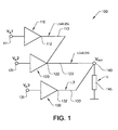
- Fig 1 shows a schematic view of a first embodiment 100 of a multi stage amplifier of the invention: as can be seen here, the multi stage amplifier 100 of the invention in this embodiment comprises a first sub-amplifier 110, which has an input port 111 and an output port 112.
- the multi stage amplifier 100 also comprises a second sub amplifier 120, which has an input port 121 and an output port 122. As can be seen in fig 1 , the output port 112 of the first sub-amplifier 110 is connected to the output port 122 of the second sub-amplifier 120 via a connection 113 which has an electrical length L1.
- the output port 122 of the second sub-amplifier is connected to a common output port 140 for the entire multi-stage amplifier 100 via a connection 123 which has an electrical length L2. Also shown symbolically in fig 1 is an external load L, shown as 145, to which the multi stage amplifier 100 is connected.
- the multi stage amplifier 100 of the invention also comprises a third sub-amplifier 130, with an input port 131 and an output port 132.
- the output port 132 of the third sub-amplifier 130 is connected to the common output port 140 via a connection 133 with an electrical length L3.
- the first sub-amplifier 110 should generally be smaller than the second sub-amplifier 120 in terms of peak output power
- the first sub-amplifier 110 may also be seen as an “outer” sub-amplifier in the circuit 100, while the second sub-amplifier 120 is seen as an “inner” sub-amplifier in the same circuit 100.
- the electrical lengths L1 and L2 are chosen so that their combination gives a useful load transformation for the outer sub-amplifier 110, while allowing the inner sub-amplifier 120 to contribute efficiently in the upper amplitude region.
- the electrical length L3 in the second branch is chosen so that it complements the effective electrical length L1 or L2. This determines if Chireix characteristics are obtained by the multi stage amplifier 100 in a lower or an upper amplitude region, or in both amplitude regions. More specific examples of this length will be given in the following.
- [L1, L2] [0.35, 0.35] or [0.15, 0.15] or [0.35, 0.15] or [0.15, 0.35] or [0.2, 0.2], expressed as wavelengths, ⁇ , of the frequency for which the multi-stage amplifier is intended to operate.
- a suitable length for L3 is that the sum of the electrical lengths L3 and L1 is one half wavelength, ⁇ , of the frequency for which the multi-stage amplifier is intended to operate.
- Chireix action is obtained between the first 110 and second 120 sub-amplifiers and the third sub-amplifier 130.
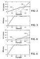
- Fig 2 shows the RF currents in the three sub-amplifiers as a function of the amplitude which is obtained by the electrical lengths in the example given in (1) above
- fig 3 shows the efficiency of the entire multi stage amplifier 100 as a function of amplitude with the electrical length of (1) above.
- the first sub-amplifier 110 draws considerably less current than the other two sub-amplifiers 120, 130 at higher amplitudes.
- the multi stage amplifier 100 As an alternative to the electrical lengths described above in (1), it is also possible to design the multi stage amplifier 100 with electrical lengths L1, L2 and L3 which are the complementary lengths to those stated in (1) above, i.e. electrical lengths L1, L2 and L3 which each is 0.5 ⁇ minus the lengths stated above in (1). This will yield the same current and efficiency as those shown in fig 2 , but the phase movements of the sub-amplifiers will be reversed.
- the first sub-amplifier 110 is the only one which is active at the lower output amplitudes. This is the same irrespective of the electrical lengths chosen, i.e. either those given above or their complementary lengths.
- Fig 4 shows the current vs. amplitude behaviour of the sub-amplifiers in this case, i.e. with the electrical lengths of (2) above;
- fig 5 shows the efficiency vs. amplitude of the entire multi-stage amplifier if the electrical lengths are chose as described in that case, i.e. (2) above.
- the third sub-amplifier 130 is the one that is active in the lower amplitude regions, and as seen in fig 5 , a high degree of efficiency is obtained in this embodiment as well.
- L1 and L2 are chosen so that one of them is chosen from one of the following ranges, and the other is chosen from the other of the following ranges: [0.02-0.23], [0.27-0.48], with the lengths in the ranges being expressed as wavelengths, ⁇ , of the frequency at which the multi-stage amplifier is intended to operate.
- L1 is chosen from the range [0.02-0.23]
- L2 should be chosen from the range [0.27-0.48], and vice versa.
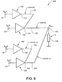
- the multi-stage amplifier comprises a fourth sub-amplifier 140, which has an input port 141 and an output port 142.
- the output port 142 of the fourth sub-amplifier 140 is connected to the output port 132 of the third sub-amplifier 130 by means of a connection which has an electrical length L4.
- first 110 and second 120 sub-amplifiers form a first "branch" of the multi-stage amplifier 200 which is essentially duplicated by a similar second "branch” formed by the third 130 and fourth 140 sub-amplifiers.
- a multi stage amplifier of the present invention can comprise a number of sub-amplifiers which is more or less arbitrary; in the case of an odd number of sub-amplifiers, the principles used for the multi-stage amplifier shown in fig 1 should be adhered to, i.e. a number of "branches" like the branch formed by the first 110 and second 120 sub-amplifier and an "outer" sub-amplifier connected as the third sub-amplifier 130 in fig 1 .
- the current vs. amplitude characteristics of the first pair of sub-amplifiers 110,140 and the second pair of sub-amplifiers 120,130 are shown in fig 7 .
- sub-amplifiers 110, 140 are the ones that are active at lower amplitudes, and that this pair of sub-amplifiers draws much less current than the other pair at higher amplitudes.
- Fig 8 shows the efficiency vs. amplitude characteristic of the multi-stage amplifier 200 of fig 6 : as seen here, this embodiment of the invention also exhibits a high degree of efficiency.
- L4 and L1 are chosen from among the following ranges: [0.02-0.23], [0.27-0.48], in which ranges the lengths are expressed as wavelengths, A, of the frequency at which the multi-stage amplifier 200 is intended to operate.
- ranges [0.02-0.23]
- L1 should be chosen in the range [0.27-0.48], and vice versa.
- L3 and L2 are chosen from among the following ranges: [0.02-0.23], [0.27-0.48], in which ranges the lengths are expressed as wavelengths, A, of the frequency at which the multi-stage amplifier 200 is intended to operate.
- ranges [0.02-0.23]
- L2 should be chosen in the range [0.27-0.48], and vice versa.
- a useful combination of L1 and L4 is to let the sum of L1 and L4 be one half of the operational wavelength, ⁇ , of the multi-stage amplifier.
- this sub-amplifier comprises a FET-transistor, to which an LC-circuit (L1, C1 in parallel) is coupled at the drain of the transistor, and the source of the FET transistor is coupled to ground.
- the gate of the FET transistor is used as input port Vin for the sub-amplifier, and the drain is used as its output port Vout, via a capacitance C2.
- the sub-amplifiers 110, 120, 130, 140 can be designed using bipolar transistors instead of the FET-transistors which were shown in figs 9 and 10 .
Landscapes
- Engineering & Computer Science (AREA)
- Power Engineering (AREA)
- Amplifiers (AREA)
Claims (12)
- Mehrstufenverstärker (100), umfassend einen ersten (110), einen zweiten (120) und einen dritten (130) Unterverstärker, die jeweils jeweilige Eingangs- (111, 121, 131) und Ausgangs- (112, 122, 132) Anschlüsse aufweisen, wobei der Mehrstufenverstärker (100) ebenfalls einen gemeinsamen Ausgangsanschluss (140) aufweist, in welchem Mehrstufenverstärker der Ausgangsanschluss (122) des zweiten Unterverstärkers (120) über eine Verbindung (113) mit einer ersten elektrischen Länge L1 mit dem Ausgangsanschluss (112) des ersten Unterverstärkers (110) verbunden ist und über eine andere Verbindung (123) mit einer zweiten elektrischen Länge L2 zu dem gemeinsamen Ausgangsanschluss (140) des Mehrstufenverstärkers verbunden ist, und der Ausgangsanschluss (132) des dritten Unterverstärkers (130) über eine dritte Verbindung (133) mit einer dritten elektrischen Länge L3 zu dem gemeinsamen Ausgangsanschluss (140) verbunden ist, wobei der Mehrstufenverstärker (200) gekennzeichnet ist dadurch, dass die elektrische Länge L1, L2 der Verbindungen von dem Ausgangsanschluss des zweiten Unterverstärkers (122) sowohl zu dem Ausgangsanschluss (112) des ersten Verstärkers und zu dem gemeinsamen Ausgangsanschluss (140) länger oder kürzer als ein Viertel einer Wellenlänge (λ) der Frequenz ist, für welche der Mehrstufenverstärker (100) gedacht ist zu operieren.
- Mehrstufenverstärker (100) nach Anspruch 1, in welchem die elektrischen Längen L1, L2 der Verbindungen von dem Ausgangsanschluss (122) des zweiten Unterverstärkers zu dem Ausgangsanschluss (112) des ersten Unterverstärkers und zu dem gemeinsamen Ausgangsanschluss ausgewählt werden unter den folgenden Kombinationen: [0.35, 0.35], [0.15, 0,15], [0.35, 0.15], [0.15, 0.35], [0.2, 0.2], ausgedrückt als Wellenlängen (λ) der Frequenz für welche der Mehrstufenverstärker (200) gedacht ist zu operieren.
- Mehrstufenverstärker (100) nach Anspruch 1, in welchem die Summe der elektrischen Wellenlängen L3, L1 der Verbindung von dem Ausgangsanschluss (132) des dritten Unterverstärkers zu dem gemeinsamen Ausgangsanschluss (140) und die Verbindung von dem Ausgangsanschluss (112) des ersten Verstärkers zu dem Ausgangsanschluss (122) des zweiten Verstärkers ein Halb der Betriebswellenlänge des Mehrstufenverstärker ist.
- Mehrstufenverstärker (100) nach Anspruch 1, in welchem die elektrischen Längen L1, L2 der Verbindungen von dem Ausgangsanschluss (122) des zweiten Unterverstärkers zu dem Ausgangsanschluss (112) des ersten Unterverstärkers und zu dem gemeinsamen Ausgangsanschluss ausgewählt sind, so dass eine der elektrischen Längen ausgewählt ist aus einer der folgenden Bereiche, und die andere elektrische Länge ausgewählt ist aus der anderen der folgenden Bereiche: [0.02 - 0.23], [0.27 - 0.48], wobei die Längen als Wellenlängen (λ) der Frequenz bei welcher der Mehrstufenverstärker (200) gedacht ist zu operieren, ausgedrückt ist.
- Mehrstufenverstärker (100) nach einem der Ansprüche 1 bis 4, in welchem die elektrische Länge L3 der Verbindung von dem Ausgangsanschluss (132) des dritten Unterverstärkers zu dem gemeinsamen Ausgangsanschluss (140) 0.18λ, 0,29λ oder 0.32λ ist, wobei λ die Wellenlänge ist, bei welcher der Mehrstufenverstärker (100) gedacht ist zu operieren.
- Mehrstufenverstärker (200) nach einem der Ansprüche 1 bis 5, ferner umfassend einen vierten Unterverstärker (140) mit einem Eingangsanschluss (141) und einem Ausgangsanschluss (142), welcher über eine Verbindung mit einer elektrischen Länge L4 zu dem Ausgangsanschluss (133) des dritten Unterverstärkers (130) verbunden ist.
- Mehrstufenverstärker nach Anspruch 6, in welchem die elektrischen Längen L4, L1 der Verbindung von dem Ausgangsanschluss (142) des vierten Unterverstärkers zu dem Ausgangsanschluss (132) des dritten Unterverstärkers und die Verbindung von dem Ausgangsanschluss (112) des erste Unterverstärkers zu dem Ausgangsanschluss (122) des zweiten Unterverstärkers ausgewählt sind aus den folgenden Bereichen: [0.02 - 0.23], [0.27 - 0.48], in welchen Bereichen die Längen ausgedrückt sind als Wellenlängen (λ) der Frequenz, bei welchem der Mehrstufenverstärker (200) gedacht ist zu operieren.
- Mehrstufenverstärker nach Anspruch 6 oder 7, in welchem die Summe der elektrischen Längen L3, L2 der Verbindung von dem Ausgangsanschluss (132) des dritten Unterverstärkers zu dem gemeinsamen Ausgangsanschluss (140) und die Verbindung von dem Ausgangsanschluss (122) des zweiten Unterverstärkers zu dem gemeinsamen Ausgangsanschluss (140) des Mehrstufenverstärkers ausgewählt sind aus den folgenden Bereichen: [0.02 - 0.23], [0.27 - 0.48], in welchen Bereichen die Längen ausgedrückt sind als Wellenlängen (λ) der Frequenz, bei welchem der Mehrstufenverstärker (200) gedacht ist zu operieren.
- Mehrstufenverstärker nach einem der Ansprüche 6 bis 8, in welchem die Summe der elektrischen Längen L4, L1 der Verbindung von dem Ausgangsanschluss (142) des vierten Unterverstärkers zu dem Ausgangsanschluss (132) des dritten Unterverstärkers und die Verbindung von dem Ausgangsanschluss (112) des ersten Unterverstärkers zu dem Ausgangsanschluss (122) des zweiten Unterverstärkers ein Halb der Betriebswellenlänge (λ) des Mehrstufenverstärkers ist.
- Mehrstufenverstärker nach einem der Ansprüche 6 bis 9, in welchem die Summe der elektrischen Längen L3, L2 der Verbindung von dem Ausgangsanschluss (132) des dritten Unterverstärkers zu dem gemeinsamen Ausgangsanschluss (140) und die Verbindung von dem Ausgangsanschluss (122) des zweiten Unterverstärkers zu dem gemeinsamen Ausgangsanschluss (140) des Mehrstufenverstärkers ein Halb der Betriebswellenlänge des Mehrstufenverstärkers ist.
- Mehrstufenverstärker (100, 200) nach einem der vorangegangenen Ansprüche, in welchem mindestens einer der Unterverstärker einen FET-Transistor umfasst.
- Mehrstufenverstärker (100, 200) nach einem der Ansprüche 1 bis 11, in welchem mindestens einer der Unterverstärker einen Bipolar-Transistor umfasst.
Applications Claiming Priority (1)
| Application Number | Priority Date | Filing Date | Title |
|---|---|---|---|
| PCT/SE2008/051545 WO2010074615A1 (en) | 2008-12-22 | 2008-12-22 | A multi stage amplifier |
Publications (2)
| Publication Number | Publication Date |
|---|---|
| EP2380276A1 EP2380276A1 (de) | 2011-10-26 |
| EP2380276B1 true EP2380276B1 (de) | 2012-10-10 |
Family
ID=40834282
Family Applications (1)
| Application Number | Title | Priority Date | Filing Date |
|---|---|---|---|
| EP08876327A Not-in-force EP2380276B1 (de) | 2008-12-22 | 2008-12-22 | Mehrstufiger verstärker |
Country Status (3)
| Country | Link |
|---|---|
| US (1) | US8305146B2 (de) |
| EP (1) | EP2380276B1 (de) |
| WO (1) | WO2010074615A1 (de) |
Families Citing this family (5)
| Publication number | Priority date | Publication date | Assignee | Title |
|---|---|---|---|---|
| JP5237462B2 (ja) | 2008-12-09 | 2013-07-17 | テレフオンアクチーボラゲット エル エム エリクソン(パブル) | 多段増幅器 |
| US20160241201A1 (en) | 2013-10-18 | 2016-08-18 | Telefonaktiebolaget Lm Ericsson (Publ) | Power amplifier for amplification of an input signal into an output signal |
| US9577584B2 (en) | 2014-05-08 | 2017-02-21 | Telefonaktiebolaget Lm Ericsson (Publ) | Amplifier circuit and method |
| WO2015171026A1 (en) | 2014-05-08 | 2015-11-12 | Telefonaktiebolaget L M Ericsson (Publ) | Amplifier circuit and method |
| US10205424B2 (en) | 2015-05-12 | 2019-02-12 | Telefonaktiebolaget Lm Ericsson (Publ) | Composite power amplifier |
Family Cites Families (7)
| Publication number | Priority date | Publication date | Assignee | Title |
|---|---|---|---|---|
| US5025225A (en) * | 1989-12-15 | 1991-06-18 | Raytheon Company | Amplifier having substantially constant D.C. to r.f. conversion efficiency |
| US5543751A (en) * | 1995-07-21 | 1996-08-06 | Motorola, Inc. | Power combiner for use in a radio frequency system and a method of constructing a power combiner |
| AU2002334520A1 (en) * | 2002-09-06 | 2004-03-29 | Telefonaktiebolaget L M Ericsson (Publ) | Composite power amplifier |
| WO2004057755A1 (en) * | 2002-12-19 | 2004-07-08 | Telefonaktiebolaget Lm Ericsson | Composite amplifier structure |
| US8130043B2 (en) * | 2003-09-25 | 2012-03-06 | Anadigics, Inc. | Multi-stage power amplifier with enhanced efficiency |
| SE0302586D0 (sv) * | 2003-09-26 | 2003-09-26 | Ericsson Telefon Ab L M | Composite power amplifier |
| EP2216901B1 (de) * | 2005-12-30 | 2012-02-08 | Telefonaktiebolaget L M Ericsson (Publ) | Effizienter zusammengesetzter Verstärker |
-
2008
- 2008-12-22 EP EP08876327A patent/EP2380276B1/de not_active Not-in-force
- 2008-12-22 WO PCT/SE2008/051545 patent/WO2010074615A1/en not_active Ceased
- 2008-12-22 US US13/141,636 patent/US8305146B2/en not_active Expired - Fee Related
Also Published As
| Publication number | Publication date |
|---|---|
| US20110254629A1 (en) | 2011-10-20 |
| WO2010074615A1 (en) | 2010-07-01 |
| EP2380276A1 (de) | 2011-10-26 |
| US8305146B2 (en) | 2012-11-06 |
Similar Documents
| Publication | Publication Date | Title |
|---|---|---|
| EP3439172B1 (de) | Vierwege-doherty-verstärker und mobilfunkkommunikationsbasisstation | |
| CN102237852B (zh) | 功率放大器 | |
| EP2876810B1 (de) | Doherty-Verstärker | |
| KR101595739B1 (ko) | 전력 증폭기 | |
| US20100244955A1 (en) | Reconfigurable Distributed Active Transformers | |
| EP2451074B1 (de) | Verstärker | |
| EP2403135A1 (de) | Leistungsverstärker für mobile Telekommunikation | |
| KR101325158B1 (ko) | 다중 모드 도허티 전력 증폭 장치 | |
| EP2374210B1 (de) | Mehrstufiger verstärker | |
| KR101079474B1 (ko) | 내부 정합 인덕터를 공유하는 무선 통신을 위한 병렬 증폭 장치 | |
| US8744378B2 (en) | LINC transmitter with improved efficiency | |
| US8305146B2 (en) | Multi stage amplifier | |
| KR20130055843A (ko) | 전력 증폭기 및 그 증폭 방법 | |
| EP3205015A1 (de) | Verstärkerschaltung und verfahren | |
| WO2014193275A1 (en) | Amplifier circuit and method | |
| SE528473C2 (sv) | Monolitiskt integrerad effektförstärkaranordning | |
| KR20080037559A (ko) | 바이어스 회로 | |
| US6667670B2 (en) | Microwave double-pole double-throw switch and microwave divide/through switch and power amplifier using thereof | |
| JP4629672B2 (ja) | 高い出力パワーダイナミクスを有する増幅器 | |
| US10418947B2 (en) | Doherty amplifier | |
| US9866190B2 (en) | Multi-stage amplifiers with low loss | |
| EP1521360A1 (de) | Parallele Verstärkeranordnung | |
| JP2011082809A (ja) | バイアス回路 | |
| EP3140908B1 (de) | Verstärkerschaltung und verfahren | |
| EP3205016B1 (de) | Verstärkerschaltung und verfahren |
Legal Events
| Date | Code | Title | Description |
|---|---|---|---|
| PUAI | Public reference made under article 153(3) epc to a published international application that has entered the european phase |
Free format text: ORIGINAL CODE: 0009012 |
|
| 17P | Request for examination filed |
Effective date: 20110719 |
|
| AK | Designated contracting states |
Kind code of ref document: A1 Designated state(s): AT BE BG CH CY CZ DE DK EE ES FI FR GB GR HR HU IE IS IT LI LT LU LV MC MT NL NO PL PT RO SE SI SK TR |
|
| DAX | Request for extension of the european patent (deleted) | ||
| GRAP | Despatch of communication of intention to grant a patent |
Free format text: ORIGINAL CODE: EPIDOSNIGR1 |
|
| GRAS | Grant fee paid |
Free format text: ORIGINAL CODE: EPIDOSNIGR3 |
|
| GRAA | (expected) grant |
Free format text: ORIGINAL CODE: 0009210 |
|
| RAP1 | Party data changed (applicant data changed or rights of an application transferred) |
Owner name: TELEFONAKTIEBOLAGET L M ERICSSON (PUBL) |
|
| AK | Designated contracting states |
Kind code of ref document: B1 Designated state(s): AT BE BG CH CY CZ DE DK EE ES FI FR GB GR HR HU IE IS IT LI LT LU LV MC MT NL NO PL PT RO SE SI SK TR |
|
| REG | Reference to a national code |
Ref country code: GB Ref legal event code: FG4D |
|
| REG | Reference to a national code |
Ref country code: AT Ref legal event code: REF Ref document number: 579348 Country of ref document: AT Kind code of ref document: T Effective date: 20121015 Ref country code: CH Ref legal event code: EP |
|
| REG | Reference to a national code |
Ref country code: IE Ref legal event code: FG4D |
|
| REG | Reference to a national code |
Ref country code: DE Ref legal event code: R096 Ref document number: 602008019359 Country of ref document: DE Effective date: 20121213 |
|
| PG25 | Lapsed in a contracting state [announced via postgrant information from national office to epo] |
Ref country code: SI Free format text: LAPSE BECAUSE OF FAILURE TO SUBMIT A TRANSLATION OF THE DESCRIPTION OR TO PAY THE FEE WITHIN THE PRESCRIBED TIME-LIMIT Effective date: 20121010 |
|
| REG | Reference to a national code |
Ref country code: NL Ref legal event code: VDEP Effective date: 20121010 |
|
| REG | Reference to a national code |
Ref country code: AT Ref legal event code: MK05 Ref document number: 579348 Country of ref document: AT Kind code of ref document: T Effective date: 20121010 |
|
| REG | Reference to a national code |
Ref country code: LT Ref legal event code: MG4D |
|
| PG25 | Lapsed in a contracting state [announced via postgrant information from national office to epo] |
Ref country code: NL Free format text: LAPSE BECAUSE OF FAILURE TO SUBMIT A TRANSLATION OF THE DESCRIPTION OR TO PAY THE FEE WITHIN THE PRESCRIBED TIME-LIMIT Effective date: 20121010 Ref country code: HR Free format text: LAPSE BECAUSE OF FAILURE TO SUBMIT A TRANSLATION OF THE DESCRIPTION OR TO PAY THE FEE WITHIN THE PRESCRIBED TIME-LIMIT Effective date: 20121010 Ref country code: FI Free format text: LAPSE BECAUSE OF FAILURE TO SUBMIT A TRANSLATION OF THE DESCRIPTION OR TO PAY THE FEE WITHIN THE PRESCRIBED TIME-LIMIT Effective date: 20121010 Ref country code: NO Free format text: LAPSE BECAUSE OF FAILURE TO SUBMIT A TRANSLATION OF THE DESCRIPTION OR TO PAY THE FEE WITHIN THE PRESCRIBED TIME-LIMIT Effective date: 20130110 Ref country code: LT Free format text: LAPSE BECAUSE OF FAILURE TO SUBMIT A TRANSLATION OF THE DESCRIPTION OR TO PAY THE FEE WITHIN THE PRESCRIBED TIME-LIMIT Effective date: 20121010 Ref country code: IS Free format text: LAPSE BECAUSE OF FAILURE TO SUBMIT A TRANSLATION OF THE DESCRIPTION OR TO PAY THE FEE WITHIN THE PRESCRIBED TIME-LIMIT Effective date: 20130210 Ref country code: SE Free format text: LAPSE BECAUSE OF FAILURE TO SUBMIT A TRANSLATION OF THE DESCRIPTION OR TO PAY THE FEE WITHIN THE PRESCRIBED TIME-LIMIT Effective date: 20121010 |
|
| PG25 | Lapsed in a contracting state [announced via postgrant information from national office to epo] |
Ref country code: BE Free format text: LAPSE BECAUSE OF FAILURE TO SUBMIT A TRANSLATION OF THE DESCRIPTION OR TO PAY THE FEE WITHIN THE PRESCRIBED TIME-LIMIT Effective date: 20121010 Ref country code: GR Free format text: LAPSE BECAUSE OF FAILURE TO SUBMIT A TRANSLATION OF THE DESCRIPTION OR TO PAY THE FEE WITHIN THE PRESCRIBED TIME-LIMIT Effective date: 20130111 Ref country code: PT Free format text: LAPSE BECAUSE OF FAILURE TO SUBMIT A TRANSLATION OF THE DESCRIPTION OR TO PAY THE FEE WITHIN THE PRESCRIBED TIME-LIMIT Effective date: 20130211 Ref country code: LV Free format text: LAPSE BECAUSE OF FAILURE TO SUBMIT A TRANSLATION OF THE DESCRIPTION OR TO PAY THE FEE WITHIN THE PRESCRIBED TIME-LIMIT Effective date: 20121010 Ref country code: PL Free format text: LAPSE BECAUSE OF FAILURE TO SUBMIT A TRANSLATION OF THE DESCRIPTION OR TO PAY THE FEE WITHIN THE PRESCRIBED TIME-LIMIT Effective date: 20121010 |
|
| PG25 | Lapsed in a contracting state [announced via postgrant information from national office to epo] |
Ref country code: AT Free format text: LAPSE BECAUSE OF FAILURE TO SUBMIT A TRANSLATION OF THE DESCRIPTION OR TO PAY THE FEE WITHIN THE PRESCRIBED TIME-LIMIT Effective date: 20121010 |
|
| PG25 | Lapsed in a contracting state [announced via postgrant information from national office to epo] |
Ref country code: BG Free format text: LAPSE BECAUSE OF FAILURE TO SUBMIT A TRANSLATION OF THE DESCRIPTION OR TO PAY THE FEE WITHIN THE PRESCRIBED TIME-LIMIT Effective date: 20130110 Ref country code: SK Free format text: LAPSE BECAUSE OF FAILURE TO SUBMIT A TRANSLATION OF THE DESCRIPTION OR TO PAY THE FEE WITHIN THE PRESCRIBED TIME-LIMIT Effective date: 20121010 Ref country code: DK Free format text: LAPSE BECAUSE OF FAILURE TO SUBMIT A TRANSLATION OF THE DESCRIPTION OR TO PAY THE FEE WITHIN THE PRESCRIBED TIME-LIMIT Effective date: 20121010 Ref country code: EE Free format text: LAPSE BECAUSE OF FAILURE TO SUBMIT A TRANSLATION OF THE DESCRIPTION OR TO PAY THE FEE WITHIN THE PRESCRIBED TIME-LIMIT Effective date: 20121010 Ref country code: MC Free format text: LAPSE BECAUSE OF NON-PAYMENT OF DUE FEES Effective date: 20121231 Ref country code: CZ Free format text: LAPSE BECAUSE OF FAILURE TO SUBMIT A TRANSLATION OF THE DESCRIPTION OR TO PAY THE FEE WITHIN THE PRESCRIBED TIME-LIMIT Effective date: 20121010 |
|
| REG | Reference to a national code |
Ref country code: CH Ref legal event code: PL |
|
| PLBE | No opposition filed within time limit |
Free format text: ORIGINAL CODE: 0009261 |
|
| STAA | Information on the status of an ep patent application or granted ep patent |
Free format text: STATUS: NO OPPOSITION FILED WITHIN TIME LIMIT |
|
| PG25 | Lapsed in a contracting state [announced via postgrant information from national office to epo] |
Ref country code: RO Free format text: LAPSE BECAUSE OF FAILURE TO SUBMIT A TRANSLATION OF THE DESCRIPTION OR TO PAY THE FEE WITHIN THE PRESCRIBED TIME-LIMIT Effective date: 20121010 |
|
| 26N | No opposition filed |
Effective date: 20130711 |
|
| REG | Reference to a national code |
Ref country code: IE Ref legal event code: MM4A |
|
| REG | Reference to a national code |
Ref country code: FR Ref legal event code: ST Effective date: 20130830 |
|
| PG25 | Lapsed in a contracting state [announced via postgrant information from national office to epo] |
Ref country code: IE Free format text: LAPSE BECAUSE OF NON-PAYMENT OF DUE FEES Effective date: 20121222 Ref country code: CH Free format text: LAPSE BECAUSE OF NON-PAYMENT OF DUE FEES Effective date: 20121231 Ref country code: LI Free format text: LAPSE BECAUSE OF NON-PAYMENT OF DUE FEES Effective date: 20121231 Ref country code: ES Free format text: LAPSE BECAUSE OF FAILURE TO SUBMIT A TRANSLATION OF THE DESCRIPTION OR TO PAY THE FEE WITHIN THE PRESCRIBED TIME-LIMIT Effective date: 20130121 |
|
| REG | Reference to a national code |
Ref country code: DE Ref legal event code: R097 Ref document number: 602008019359 Country of ref document: DE Effective date: 20130711 |
|
| PG25 | Lapsed in a contracting state [announced via postgrant information from national office to epo] |
Ref country code: FR Free format text: LAPSE BECAUSE OF NON-PAYMENT OF DUE FEES Effective date: 20130102 Ref country code: CY Free format text: LAPSE BECAUSE OF FAILURE TO SUBMIT A TRANSLATION OF THE DESCRIPTION OR TO PAY THE FEE WITHIN THE PRESCRIBED TIME-LIMIT Effective date: 20121010 Ref country code: MT Free format text: LAPSE BECAUSE OF FAILURE TO SUBMIT A TRANSLATION OF THE DESCRIPTION OR TO PAY THE FEE WITHIN THE PRESCRIBED TIME-LIMIT Effective date: 20121010 |
|
| PG25 | Lapsed in a contracting state [announced via postgrant information from national office to epo] |
Ref country code: TR Free format text: LAPSE BECAUSE OF FAILURE TO SUBMIT A TRANSLATION OF THE DESCRIPTION OR TO PAY THE FEE WITHIN THE PRESCRIBED TIME-LIMIT Effective date: 20121010 |
|
| PG25 | Lapsed in a contracting state [announced via postgrant information from national office to epo] |
Ref country code: LU Free format text: LAPSE BECAUSE OF NON-PAYMENT OF DUE FEES Effective date: 20121222 |
|
| PG25 | Lapsed in a contracting state [announced via postgrant information from national office to epo] |
Ref country code: HU Free format text: LAPSE BECAUSE OF FAILURE TO SUBMIT A TRANSLATION OF THE DESCRIPTION OR TO PAY THE FEE WITHIN THE PRESCRIBED TIME-LIMIT Effective date: 20081222 |
|
| PG25 | Lapsed in a contracting state [announced via postgrant information from national office to epo] |
Ref country code: IT Free format text: LAPSE BECAUSE OF NON-PAYMENT OF DUE FEES Effective date: 20151222 |
|
| PG25 | Lapsed in a contracting state [announced via postgrant information from national office to epo] |
Ref country code: IT Free format text: LAPSE BECAUSE OF NON-PAYMENT OF DUE FEES Effective date: 20151222 |
|
| PGFP | Annual fee paid to national office [announced via postgrant information from national office to epo] |
Ref country code: IT Payment date: 20161222 Year of fee payment: 9 |
|
| PGRI | Patent reinstated in contracting state [announced from national office to epo] |
Ref country code: IT Effective date: 20170710 |
|
| PG25 | Lapsed in a contracting state [announced via postgrant information from national office to epo] |
Ref country code: IT Free format text: LAPSE BECAUSE OF NON-PAYMENT OF DUE FEES Effective date: 20171222 |
|
| PGFP | Annual fee paid to national office [announced via postgrant information from national office to epo] |
Ref country code: DE Payment date: 20211227 Year of fee payment: 14 Ref country code: GB Payment date: 20211227 Year of fee payment: 14 |
|
| REG | Reference to a national code |
Ref country code: DE Ref legal event code: R119 Ref document number: 602008019359 Country of ref document: DE |
|
| GBPC | Gb: european patent ceased through non-payment of renewal fee |
Effective date: 20221222 |
|
| PG25 | Lapsed in a contracting state [announced via postgrant information from national office to epo] |
Ref country code: GB Free format text: LAPSE BECAUSE OF NON-PAYMENT OF DUE FEES Effective date: 20221222 Ref country code: DE Free format text: LAPSE BECAUSE OF NON-PAYMENT OF DUE FEES Effective date: 20230701 |