EP2381013A2 - Kohlenstoffkomponente und Herstellungsverfahren dafür - Google Patents
Kohlenstoffkomponente und Herstellungsverfahren dafür Download PDFInfo
- Publication number
- EP2381013A2 EP2381013A2 EP11163167A EP11163167A EP2381013A2 EP 2381013 A2 EP2381013 A2 EP 2381013A2 EP 11163167 A EP11163167 A EP 11163167A EP 11163167 A EP11163167 A EP 11163167A EP 2381013 A2 EP2381013 A2 EP 2381013A2
- Authority
- EP
- European Patent Office
- Prior art keywords
- carbon
- hole
- ceramic coating
- plate members
- mating
- Prior art date
- Legal status (The legal status is an assumption and is not a legal conclusion. Google has not performed a legal analysis and makes no representation as to the accuracy of the status listed.)
- Withdrawn
Links
Images


Classifications
-
- C—CHEMISTRY; METALLURGY
- C04—CEMENTS; CONCRETE; ARTIFICIAL STONE; CERAMICS; REFRACTORIES
- C04B—LIME, MAGNESIA; SLAG; CEMENTS; COMPOSITIONS THEREOF, e.g. MORTARS, CONCRETE OR LIKE BUILDING MATERIALS; ARTIFICIAL STONE; CERAMICS; REFRACTORIES; TREATMENT OF NATURAL STONE
- C04B41/00—After-treatment of mortars, concrete, artificial stone or ceramics; Treatment of natural stone
- C04B41/009—After-treatment of mortars, concrete, artificial stone or ceramics; Treatment of natural stone characterised by the material treated
-
- C—CHEMISTRY; METALLURGY
- C04—CEMENTS; CONCRETE; ARTIFICIAL STONE; CERAMICS; REFRACTORIES
- C04B—LIME, MAGNESIA; SLAG; CEMENTS; COMPOSITIONS THEREOF, e.g. MORTARS, CONCRETE OR LIKE BUILDING MATERIALS; ARTIFICIAL STONE; CERAMICS; REFRACTORIES; TREATMENT OF NATURAL STONE
- C04B37/00—Joining burned ceramic articles with other burned ceramic articles or other articles by heating
- C04B37/003—Joining burned ceramic articles with other burned ceramic articles or other articles by heating by means of an interlayer consisting of a combination of materials selected from glass, or ceramic material with metals, metal oxides or metal salts
- C04B37/005—Joining burned ceramic articles with other burned ceramic articles or other articles by heating by means of an interlayer consisting of a combination of materials selected from glass, or ceramic material with metals, metal oxides or metal salts consisting of glass or ceramic material
-
- C—CHEMISTRY; METALLURGY
- C04—CEMENTS; CONCRETE; ARTIFICIAL STONE; CERAMICS; REFRACTORIES
- C04B—LIME, MAGNESIA; SLAG; CEMENTS; COMPOSITIONS THEREOF, e.g. MORTARS, CONCRETE OR LIKE BUILDING MATERIALS; ARTIFICIAL STONE; CERAMICS; REFRACTORIES; TREATMENT OF NATURAL STONE
- C04B37/00—Joining burned ceramic articles with other burned ceramic articles or other articles by heating
- C04B37/008—Joining burned ceramic articles with other burned ceramic articles or other articles by heating by means of an interlayer consisting of an organic adhesive, e.g. phenol resin or pitch
-
- C—CHEMISTRY; METALLURGY
- C04—CEMENTS; CONCRETE; ARTIFICIAL STONE; CERAMICS; REFRACTORIES
- C04B—LIME, MAGNESIA; SLAG; CEMENTS; COMPOSITIONS THEREOF, e.g. MORTARS, CONCRETE OR LIKE BUILDING MATERIALS; ARTIFICIAL STONE; CERAMICS; REFRACTORIES; TREATMENT OF NATURAL STONE
- C04B41/00—After-treatment of mortars, concrete, artificial stone or ceramics; Treatment of natural stone
- C04B41/45—Coating or impregnating, e.g. injection in masonry, partial coating of green or fired ceramics, organic coating compositions for adhering together two concrete elements
- C04B41/50—Coating or impregnating, e.g. injection in masonry, partial coating of green or fired ceramics, organic coating compositions for adhering together two concrete elements with inorganic materials
- C04B41/5053—Coating or impregnating, e.g. injection in masonry, partial coating of green or fired ceramics, organic coating compositions for adhering together two concrete elements with inorganic materials non-oxide ceramics
- C04B41/5057—Carbides
- C04B41/5059—Silicon carbide
-
- C—CHEMISTRY; METALLURGY
- C04—CEMENTS; CONCRETE; ARTIFICIAL STONE; CERAMICS; REFRACTORIES
- C04B—LIME, MAGNESIA; SLAG; CEMENTS; COMPOSITIONS THEREOF, e.g. MORTARS, CONCRETE OR LIKE BUILDING MATERIALS; ARTIFICIAL STONE; CERAMICS; REFRACTORIES; TREATMENT OF NATURAL STONE
- C04B41/00—After-treatment of mortars, concrete, artificial stone or ceramics; Treatment of natural stone
- C04B41/45—Coating or impregnating, e.g. injection in masonry, partial coating of green or fired ceramics, organic coating compositions for adhering together two concrete elements
- C04B41/50—Coating or impregnating, e.g. injection in masonry, partial coating of green or fired ceramics, organic coating compositions for adhering together two concrete elements with inorganic materials
- C04B41/5053—Coating or impregnating, e.g. injection in masonry, partial coating of green or fired ceramics, organic coating compositions for adhering together two concrete elements with inorganic materials non-oxide ceramics
- C04B41/5062—Borides, Nitrides or Silicides
- C04B41/5064—Boron nitride
-
- C—CHEMISTRY; METALLURGY
- C04—CEMENTS; CONCRETE; ARTIFICIAL STONE; CERAMICS; REFRACTORIES
- C04B—LIME, MAGNESIA; SLAG; CEMENTS; COMPOSITIONS THEREOF, e.g. MORTARS, CONCRETE OR LIKE BUILDING MATERIALS; ARTIFICIAL STONE; CERAMICS; REFRACTORIES; TREATMENT OF NATURAL STONE
- C04B41/00—After-treatment of mortars, concrete, artificial stone or ceramics; Treatment of natural stone
- C04B41/80—After-treatment of mortars, concrete, artificial stone or ceramics; Treatment of natural stone of only ceramics
- C04B41/81—Coating or impregnation
- C04B41/85—Coating or impregnation with inorganic materials
- C04B41/87—Ceramics
-
- C—CHEMISTRY; METALLURGY
- C23—COATING METALLIC MATERIAL; COATING MATERIAL WITH METALLIC MATERIAL; CHEMICAL SURFACE TREATMENT; DIFFUSION TREATMENT OF METALLIC MATERIAL; COATING BY VACUUM EVAPORATION, BY SPUTTERING, BY ION IMPLANTATION OR BY CHEMICAL VAPOUR DEPOSITION, IN GENERAL; INHIBITING CORROSION OF METALLIC MATERIAL OR INCRUSTATION IN GENERAL
- C23C—COATING METALLIC MATERIAL; COATING MATERIAL WITH METALLIC MATERIAL; SURFACE TREATMENT OF METALLIC MATERIAL BY DIFFUSION INTO THE SURFACE, BY CHEMICAL CONVERSION OR SUBSTITUTION; COATING BY VACUUM EVAPORATION, BY SPUTTERING, BY ION IMPLANTATION OR BY CHEMICAL VAPOUR DEPOSITION, IN GENERAL
- C23C14/00—Coating by vacuum evaporation, by sputtering or by ion implantation of the coating forming material
- C23C14/22—Coating by vacuum evaporation, by sputtering or by ion implantation of the coating forming material characterised by the process of coating
- C23C14/50—Substrate holders
- C23C14/505—Substrate holders for rotation of the substrates
-
- C—CHEMISTRY; METALLURGY
- C23—COATING METALLIC MATERIAL; COATING MATERIAL WITH METALLIC MATERIAL; CHEMICAL SURFACE TREATMENT; DIFFUSION TREATMENT OF METALLIC MATERIAL; COATING BY VACUUM EVAPORATION, BY SPUTTERING, BY ION IMPLANTATION OR BY CHEMICAL VAPOUR DEPOSITION, IN GENERAL; INHIBITING CORROSION OF METALLIC MATERIAL OR INCRUSTATION IN GENERAL
- C23C—COATING METALLIC MATERIAL; COATING MATERIAL WITH METALLIC MATERIAL; SURFACE TREATMENT OF METALLIC MATERIAL BY DIFFUSION INTO THE SURFACE, BY CHEMICAL CONVERSION OR SUBSTITUTION; COATING BY VACUUM EVAPORATION, BY SPUTTERING, BY ION IMPLANTATION OR BY CHEMICAL VAPOUR DEPOSITION, IN GENERAL
- C23C16/00—Chemical coating by decomposition of gaseous compounds, without leaving reaction products of surface material in the coating, i.e. chemical vapour deposition [CVD] processes
- C23C16/44—Chemical coating by decomposition of gaseous compounds, without leaving reaction products of surface material in the coating, i.e. chemical vapour deposition [CVD] processes characterised by the method of coating
- C23C16/458—Chemical coating by decomposition of gaseous compounds, without leaving reaction products of surface material in the coating, i.e. chemical vapour deposition [CVD] processes characterised by the method of coating characterised by the method used for supporting substrates in the reaction chamber
- C23C16/4581—Chemical coating by decomposition of gaseous compounds, without leaving reaction products of surface material in the coating, i.e. chemical vapour deposition [CVD] processes characterised by the method of coating characterised by the method used for supporting substrates in the reaction chamber characterised by material of construction or surface finish of the means for supporting the substrate
-
- C—CHEMISTRY; METALLURGY
- C23—COATING METALLIC MATERIAL; COATING MATERIAL WITH METALLIC MATERIAL; CHEMICAL SURFACE TREATMENT; DIFFUSION TREATMENT OF METALLIC MATERIAL; COATING BY VACUUM EVAPORATION, BY SPUTTERING, BY ION IMPLANTATION OR BY CHEMICAL VAPOUR DEPOSITION, IN GENERAL; INHIBITING CORROSION OF METALLIC MATERIAL OR INCRUSTATION IN GENERAL
- C23C—COATING METALLIC MATERIAL; COATING MATERIAL WITH METALLIC MATERIAL; SURFACE TREATMENT OF METALLIC MATERIAL BY DIFFUSION INTO THE SURFACE, BY CHEMICAL CONVERSION OR SUBSTITUTION; COATING BY VACUUM EVAPORATION, BY SPUTTERING, BY ION IMPLANTATION OR BY CHEMICAL VAPOUR DEPOSITION, IN GENERAL
- C23C16/00—Chemical coating by decomposition of gaseous compounds, without leaving reaction products of surface material in the coating, i.e. chemical vapour deposition [CVD] processes
- C23C16/44—Chemical coating by decomposition of gaseous compounds, without leaving reaction products of surface material in the coating, i.e. chemical vapour deposition [CVD] processes characterised by the method of coating
- C23C16/458—Chemical coating by decomposition of gaseous compounds, without leaving reaction products of surface material in the coating, i.e. chemical vapour deposition [CVD] processes characterised by the method of coating characterised by the method used for supporting substrates in the reaction chamber
- C23C16/4582—Rigid and flat substrates, e.g. plates or discs
- C23C16/4583—Rigid and flat substrates, e.g. plates or discs the substrate being supported substantially horizontally
- C23C16/4584—Rigid and flat substrates, e.g. plates or discs the substrate being supported substantially horizontally the substrate being rotated
-
- C—CHEMISTRY; METALLURGY
- C23—COATING METALLIC MATERIAL; COATING MATERIAL WITH METALLIC MATERIAL; CHEMICAL SURFACE TREATMENT; DIFFUSION TREATMENT OF METALLIC MATERIAL; COATING BY VACUUM EVAPORATION, BY SPUTTERING, BY ION IMPLANTATION OR BY CHEMICAL VAPOUR DEPOSITION, IN GENERAL; INHIBITING CORROSION OF METALLIC MATERIAL OR INCRUSTATION IN GENERAL
- C23C—COATING METALLIC MATERIAL; COATING MATERIAL WITH METALLIC MATERIAL; SURFACE TREATMENT OF METALLIC MATERIAL BY DIFFUSION INTO THE SURFACE, BY CHEMICAL CONVERSION OR SUBSTITUTION; COATING BY VACUUM EVAPORATION, BY SPUTTERING, BY ION IMPLANTATION OR BY CHEMICAL VAPOUR DEPOSITION, IN GENERAL
- C23C16/00—Chemical coating by decomposition of gaseous compounds, without leaving reaction products of surface material in the coating, i.e. chemical vapour deposition [CVD] processes
- C23C16/44—Chemical coating by decomposition of gaseous compounds, without leaving reaction products of surface material in the coating, i.e. chemical vapour deposition [CVD] processes characterised by the method of coating
- C23C16/458—Chemical coating by decomposition of gaseous compounds, without leaving reaction products of surface material in the coating, i.e. chemical vapour deposition [CVD] processes characterised by the method of coating characterised by the method used for supporting substrates in the reaction chamber
- C23C16/4582—Rigid and flat substrates, e.g. plates or discs
- C23C16/4587—Rigid and flat substrates, e.g. plates or discs the substrate being supported substantially vertically
- C23C16/4588—Rigid and flat substrates, e.g. plates or discs the substrate being supported substantially vertically the substrate being rotated
-
- C—CHEMISTRY; METALLURGY
- C30—CRYSTAL GROWTH
- C30B—SINGLE-CRYSTAL GROWTH; UNIDIRECTIONAL SOLIDIFICATION OF EUTECTIC MATERIAL OR UNIDIRECTIONAL DEMIXING OF EUTECTOID MATERIAL; REFINING BY ZONE-MELTING OF MATERIAL; PRODUCTION OF A HOMOGENEOUS POLYCRYSTALLINE MATERIAL WITH DEFINED STRUCTURE; SINGLE CRYSTALS OR HOMOGENEOUS POLYCRYSTALLINE MATERIAL WITH DEFINED STRUCTURE; AFTER-TREATMENT OF SINGLE CRYSTALS OR A HOMOGENEOUS POLYCRYSTALLINE MATERIAL WITH DEFINED STRUCTURE; APPARATUS THEREFOR
- C30B25/00—Single-crystal growth by chemical reaction of reactive gases, e.g. chemical vapour-deposition growth
- C30B25/02—Epitaxial-layer growth
- C30B25/12—Substrate holders or susceptors
-
- C—CHEMISTRY; METALLURGY
- C30—CRYSTAL GROWTH
- C30B—SINGLE-CRYSTAL GROWTH; UNIDIRECTIONAL SOLIDIFICATION OF EUTECTIC MATERIAL OR UNIDIRECTIONAL DEMIXING OF EUTECTOID MATERIAL; REFINING BY ZONE-MELTING OF MATERIAL; PRODUCTION OF A HOMOGENEOUS POLYCRYSTALLINE MATERIAL WITH DEFINED STRUCTURE; SINGLE CRYSTALS OR HOMOGENEOUS POLYCRYSTALLINE MATERIAL WITH DEFINED STRUCTURE; AFTER-TREATMENT OF SINGLE CRYSTALS OR A HOMOGENEOUS POLYCRYSTALLINE MATERIAL WITH DEFINED STRUCTURE; APPARATUS THEREFOR
- C30B35/00—Apparatus not otherwise provided for, specially adapted for the growth, production or after-treatment of single crystals or of a homogeneous polycrystalline material with defined structure
-
- H—ELECTRICITY
- H10—SEMICONDUCTOR DEVICES; ELECTRIC SOLID-STATE DEVICES NOT OTHERWISE PROVIDED FOR
- H10P—GENERIC PROCESSES OR APPARATUS FOR THE MANUFACTURE OR TREATMENT OF DEVICES COVERED BY CLASS H10
- H10P14/00—Formation of materials, e.g. in the shape of layers or pillars
- H10P14/20—Formation of materials, e.g. in the shape of layers or pillars of semiconductor materials
- H10P14/24—Formation of materials, e.g. in the shape of layers or pillars of semiconductor materials using chemical vapour deposition [CVD]
-
- H—ELECTRICITY
- H10—SEMICONDUCTOR DEVICES; ELECTRIC SOLID-STATE DEVICES NOT OTHERWISE PROVIDED FOR
- H10P—GENERIC PROCESSES OR APPARATUS FOR THE MANUFACTURE OR TREATMENT OF DEVICES COVERED BY CLASS H10
- H10P72/00—Handling or holding of wafers, substrates or devices during manufacture or treatment thereof
- H10P72/70—Handling or holding of wafers, substrates or devices during manufacture or treatment thereof for supporting or gripping
-
- C—CHEMISTRY; METALLURGY
- C04—CEMENTS; CONCRETE; ARTIFICIAL STONE; CERAMICS; REFRACTORIES
- C04B—LIME, MAGNESIA; SLAG; CEMENTS; COMPOSITIONS THEREOF, e.g. MORTARS, CONCRETE OR LIKE BUILDING MATERIALS; ARTIFICIAL STONE; CERAMICS; REFRACTORIES; TREATMENT OF NATURAL STONE
- C04B2235/00—Aspects relating to ceramic starting mixtures or sintered ceramic products
- C04B2235/70—Aspects relating to sintered or melt-casted ceramic products
- C04B2235/72—Products characterised by the absence or the low content of specific components, e.g. alkali metal free alumina ceramics
-
- C—CHEMISTRY; METALLURGY
- C04—CEMENTS; CONCRETE; ARTIFICIAL STONE; CERAMICS; REFRACTORIES
- C04B—LIME, MAGNESIA; SLAG; CEMENTS; COMPOSITIONS THEREOF, e.g. MORTARS, CONCRETE OR LIKE BUILDING MATERIALS; ARTIFICIAL STONE; CERAMICS; REFRACTORIES; TREATMENT OF NATURAL STONE
- C04B2237/00—Aspects relating to ceramic laminates or to joining of ceramic articles with other articles by heating
- C04B2237/02—Aspects relating to interlayers, e.g. used to join ceramic articles with other articles by heating
- C04B2237/04—Ceramic interlayers
- C04B2237/08—Non-oxidic interlayers
- C04B2237/083—Carbide interlayers, e.g. silicon carbide interlayers
-
- C—CHEMISTRY; METALLURGY
- C04—CEMENTS; CONCRETE; ARTIFICIAL STONE; CERAMICS; REFRACTORIES
- C04B—LIME, MAGNESIA; SLAG; CEMENTS; COMPOSITIONS THEREOF, e.g. MORTARS, CONCRETE OR LIKE BUILDING MATERIALS; ARTIFICIAL STONE; CERAMICS; REFRACTORIES; TREATMENT OF NATURAL STONE
- C04B2237/00—Aspects relating to ceramic laminates or to joining of ceramic articles with other articles by heating
- C04B2237/02—Aspects relating to interlayers, e.g. used to join ceramic articles with other articles by heating
- C04B2237/04—Ceramic interlayers
- C04B2237/08—Non-oxidic interlayers
- C04B2237/086—Carbon interlayers
-
- C—CHEMISTRY; METALLURGY
- C04—CEMENTS; CONCRETE; ARTIFICIAL STONE; CERAMICS; REFRACTORIES
- C04B—LIME, MAGNESIA; SLAG; CEMENTS; COMPOSITIONS THEREOF, e.g. MORTARS, CONCRETE OR LIKE BUILDING MATERIALS; ARTIFICIAL STONE; CERAMICS; REFRACTORIES; TREATMENT OF NATURAL STONE
- C04B2237/00—Aspects relating to ceramic laminates or to joining of ceramic articles with other articles by heating
- C04B2237/30—Composition of layers of ceramic laminates or of ceramic or metallic articles to be joined by heating, e.g. Si substrates
- C04B2237/32—Ceramic
- C04B2237/36—Non-oxidic
- C04B2237/363—Carbon
-
- C—CHEMISTRY; METALLURGY
- C04—CEMENTS; CONCRETE; ARTIFICIAL STONE; CERAMICS; REFRACTORIES
- C04B—LIME, MAGNESIA; SLAG; CEMENTS; COMPOSITIONS THEREOF, e.g. MORTARS, CONCRETE OR LIKE BUILDING MATERIALS; ARTIFICIAL STONE; CERAMICS; REFRACTORIES; TREATMENT OF NATURAL STONE
- C04B2237/00—Aspects relating to ceramic laminates or to joining of ceramic articles with other articles by heating
- C04B2237/50—Processing aspects relating to ceramic laminates or to the joining of ceramic articles with other articles by heating
- C04B2237/64—Forming laminates or joined articles comprising grooves or cuts
-
- C—CHEMISTRY; METALLURGY
- C04—CEMENTS; CONCRETE; ARTIFICIAL STONE; CERAMICS; REFRACTORIES
- C04B—LIME, MAGNESIA; SLAG; CEMENTS; COMPOSITIONS THEREOF, e.g. MORTARS, CONCRETE OR LIKE BUILDING MATERIALS; ARTIFICIAL STONE; CERAMICS; REFRACTORIES; TREATMENT OF NATURAL STONE
- C04B2237/00—Aspects relating to ceramic laminates or to joining of ceramic articles with other articles by heating
- C04B2237/50—Processing aspects relating to ceramic laminates or to the joining of ceramic articles with other articles by heating
- C04B2237/72—Forming laminates or joined articles comprising at least two interlayers directly next to each other
-
- C—CHEMISTRY; METALLURGY
- C04—CEMENTS; CONCRETE; ARTIFICIAL STONE; CERAMICS; REFRACTORIES
- C04B—LIME, MAGNESIA; SLAG; CEMENTS; COMPOSITIONS THEREOF, e.g. MORTARS, CONCRETE OR LIKE BUILDING MATERIALS; ARTIFICIAL STONE; CERAMICS; REFRACTORIES; TREATMENT OF NATURAL STONE
- C04B2237/00—Aspects relating to ceramic laminates or to joining of ceramic articles with other articles by heating
- C04B2237/50—Processing aspects relating to ceramic laminates or to the joining of ceramic articles with other articles by heating
- C04B2237/86—Joining of two substrates at their largest surfaces, one surface being complete joined and covered, the other surface not, e.g. a small plate joined at it's largest surface on top of a larger plate
-
- Y—GENERAL TAGGING OF NEW TECHNOLOGICAL DEVELOPMENTS; GENERAL TAGGING OF CROSS-SECTIONAL TECHNOLOGIES SPANNING OVER SEVERAL SECTIONS OF THE IPC; TECHNICAL SUBJECTS COVERED BY FORMER USPC CROSS-REFERENCE ART COLLECTIONS [XRACs] AND DIGESTS
- Y10—TECHNICAL SUBJECTS COVERED BY FORMER USPC
- Y10T—TECHNICAL SUBJECTS COVERED BY FORMER US CLASSIFICATION
- Y10T156/00—Adhesive bonding and miscellaneous chemical manufacture
- Y10T156/10—Methods of surface bonding and/or assembly therefor
- Y10T156/1002—Methods of surface bonding and/or assembly therefor with permanent bending or reshaping or surface deformation of self sustaining lamina
- Y10T156/1039—Surface deformation only of sandwich or lamina [e.g., embossed panels]
Definitions
- the present invention relates to a carbon component and a method for manufacturing the carbon component, and more particularly, a carbon component having a ceramic coating used for a CVD susceptor having a hole for introducing a gas and a method for manufacturing the carbon component.
- a susceptor In a CVD system for epitaxially growing silicon or a compound semiconductor wafer, a susceptor has been used for mounting thereon a wafer.
- a conductive graphite base material has generally been used in the susceptor for generating heat by means of induction heating. Since graphite exhibits low electrical resistance, high heat resistance and chemical stability, it can be preferably used in such a field of CVD system.
- a process rate is important for epitaxial growth, wafers are exchanged even at a relatively high temperature before an interior of the CVD system is sufficiently cooled, so that the susceptor is exposed to the atmosphere while still remaining heated.
- the graphite is used for a base material as it is, there will arise a problem of the base material reacting with air, to thus become heavily deteriorated.
- ammonium is used as a source gas. When decomposed by heat, ammonium produces hydrogen and nitrogen. Although nitrogen is used as a source gas for a gallium nitride film, hydrogen reacts with the graphite at a high temperature, to thus produce a hydrocarbon gas, like methane. Therefore, the graphite is eroded. For this reason, in order to prevent reaction of the atmosphere or hydrogen with graphite, the susceptor made of graphite is coated with ceramic, like SiC (see, for instance, JP-B-4071919 or JP-A-2004-200436 ).
- the susceptor of such a CVD system is structured to be able to mount thereon a plurality of wafers.
- some simple susceptor has a structure for mounting thereon a plurality of wafers directly on the susceptors.
- Another susceptor has a structure, in order to enhance uniformity of film thickness of the wafer, for making a film uniform by rotating a wafer or a wafer carrier on the susceptor by utilization of a gas flow in addition to rotation of (revolution) of the entire susceptor.
- a gas is introduced into an inside of the susceptor from the outside, the gas is discharged from a vertical hole (an outlet nozzle) formed substantially at a center of a mount surface of the wafer or the wafer carrier, to thus exit while generating a vortex in a space between the wafer or the wafer carrier and the susceptor.
- the vortex of gas imparts rotational energy to the wafer, whereby the wafer can rotate on the susceptor.
- gas inlet hole is formed in the susceptor from a gas inlet part formed in a side surface of the susceptor to a neighborhood of a center of the wafer mount surface (or wafer carrier).
- the gas inlet hole is formed in the side surface of the susceptor by boring, with a drill, an elongated hole that passes through a position located immediately below the neighborhood of the center of the wafer mount surface (or the wafer carriers), boring a vertical hole for establishing a connection of the center of the wafer mount surface (or the wafer carrier) with the elongated hole, and sealing an end of the elongated hole.
- a base material used as a susceptor (referred to as a susceptor base material) is subjected to another shape machining. Further, a ceramic coating, like a SiC-CVD film, a TaC-CVD film, and a pyrolytic carbon film, is formed on a surface of the susceptor base material, thereby completing a susceptor that can be used in a CVD system for epitaxial growth.
- the susceptor base material is loaded into a CVD furnace for forming a coating.
- a silane-based source gas and a hydrocarbon-based source gas are introduced into the furnace.
- the CVD furnace used at this time is for forming a ceramic coating on a base material of graphite and is totally different from the CVD furnace for epitaxial growth.
- the source gas introduced into the CVD furnace becomes decomposed upon contacting with the hot base material, to thus build up on the base material and form a ceramic coating.
- a ceramic coating is formed at high speed on a front surface of the base material to be supplied with a source gas.
- the ceramic coating is formed at low speed on a back surface, a deep interior of a recess (hole), and the like, where the source gas is difficult to reach and a coating generally tends to become thinner.
- the source gas for a ceramic coating enters the gas inlet hole of the susceptor from a small hole, to thus proceed to a deep side while contacting and building up on the wall surface of the elongated hole. For this reason, the concentration of the supplied source gas becomes low at a deep position in the elongated hole, and the source gas hardly reaches the deep position, so that the ceramic coating might not be formed.
- the outer surface of the carbon component having such an elongated hole is protected by a ceramic coating.
- the inner surface of the elongated hole that is not protected by the ceramic coating undergoes oxidation and decomposition, and thickness reduction starts from the inner surface of the elongated hole, which causes damage that extends over the entire component with time.
- the carbon component is a susceptor having an elongated hole for epitaxial growth and if a coating is not formed over the elongated hole, the susceptor contacts the outside air at replacement of wafers, and when hydrogen is used for rotating the wafer or the wafer carrier by means of a gas vortex, an inner wall of the elongated hole becomes oxidized, decomposed, and deteriorated.
- the graphite base material is a porous material, the material does not become uniformly deteriorated from its surface, so that the deterioration is accompanied by separation of particles. For this reason, the thus-separated particles spread as graphite particles over the interior of the CVD furnace for epitaxial growth, and the particles adhere to the wafer.
- the particles will cause defects. If the particles float within a hot zone, the particles will act in the air as nuclei for depositing the source gas. Then, the nuclei are deposited on the wafer, to thus cause crystal defects.
- the present invention has been made in view of the above circumstances. Accordingly, it is an aspect of the present invention to provide a carbon component that can be used without deterioration even in an atmosphere including an oxidizing gas or a decomposable gas, and in particular, that can prevent generation of particles from the inside of an elongated hole, by forming a coating on an inner surface of the elongated hole of the carbon component.
- a carbon component having a hole therein and an outer surface covered with a ceramic coating comprises two carbon plate members joined together, wherein the hole is defined by a groove formed on a mating surface of at least one of the carbon plate members and a mating portion of the other of the carbon plate members, which opposes the groove, and wherein an inner surface of the hole including a surface of the groove is entirely covered with a ceramic coating.
- the hole is defined by the groove formed on the mating surface of at least one carbon plate member and the mating portion of the other carbon member, which opposes the groove.
- the inner surface of the hole is entirely opened.
- the mating surfaces of the respective carbon plate members are joined together by a heat resistant adhesive. Therefore, an adhered portion is sandwiched so as not to become exposed to an outer or inner surface of the carbon members covered with the ceramic coating. Therefore, the adhered portion and the base material are less likely to contact the oxidizing gas or the decomposable gas, and therefore, there is little possibility of the thickness of the carbon base material being reduced.
- the ceramic coating on the inner surface of the hole is formed so as to extend over the mating surface.
- the ceramic coating on the inner surface of the hole is formed in a portion of an area of the mating surface adjacent to the hole.
- the ceramic coating is not formed over the entire mating surface, and the ceramic coating is formed on the portion of the area of the mating surface adjacent to the hole. Comparing with a case where the ceramic coating is formed over the entire mating surface, porous graphite members can be joined together by means of the heat resistant adhesive when the ceramic coating is formed in the portion of the area of the mating surface. Therefore, strong adhesive force can be obtained. In addition, since the ceramic coating is formed in the portion of the area of the mating surface adjacent to the holes, the graphite base material is less likely to contact the reactive gas and becomes resistant to corrosion.
- the ceramic coating includes at least one of SiC, pyrolytic carbon, BN, TaN and TaC.
- a SiC coating, a BN coating, a TaN coating or a TaC coating is superior to carbon of the base material in terms of corrosion resistance to hydrogen and nitrogen. Therefore, the coatings can preferably be utilized.
- the pyrolytic carbon is made of carbon and inferior to the ceramic coating in terms of corrosion resistance but superior to the same in terms of heat resistance. Since the pyrolytic carbon is a dense material, the pyrolytic carbon is superior to the graphite base material in terms of corrosion resistance and can be preferably utilized, in particularly, a case where the carbon component is used at high temperature.
- an amount of impurity content in a base material of the carbon plate members is 20 ppm or less.
- the carbon component Since the amount of impurity content in the base material of the carbon members is 20 ppm or less, the carbon component is less susceptible to oxidation or decomposition due to catalytic action of impurities and can be used for a long period.
- the carbon component of any one of (1) to (6) is a susceptor for epitaxial growth.
- a method for manufacturing a carbon component having a hole therein and an outer surface covered with a ceramic coating comprises: preparing two carbon plate members, each having a mating surface to be joined together; forming a groove on the mating surface of at least one of the carbon plate members; purifying the carbon plate members to remove impurity from the carbon plate members; forming a ceramic coating on the groove of the at least one of the carbon plate members, a mating portion of the other of the carbon plate members, which opposes the groove, and an outer surface of the carbon plate members at least except for the mating surface; and joining the carbon plate members together while the mating surfaces oppose each other.
- the hole is defined by the groove formed on the mating surface of at least one of the carbon plate members and the a mating portion of the other carbon member, which opposes the groove.
- a ceramic coating can be reliably formed on the elongated hole, and therefore, the carbon component can be used even in an atmosphere of an oxidizing gas or a decomposable gas without being deteriorated. Further, if the carbon component of the present invention is used for a susceptor that has a gas supplying hole and a mechanism for rotating wafers, generation of carbon particles in a CVD system for epitaxial growth is reduced or prevented, and therefore, wafers having few or no defects can be supplied.
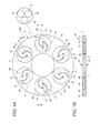
- Fig. 1A is a plan view of a carbon component according to an illustrative embodiment of the present invention
- Fig. 1B is a cross sectional view taken along line A-A shown in Fig. 1A
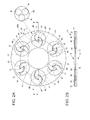
- Fig. 2A is a plan view of a modification of the carbon component shown in Fig. 1
- Fig. 2B is a cross sectional view taken along line B-B shown in Fig. 2A .
- a carbon component 100 according to an illustrative embodiment of the present invention may be preferably used as a wafer holding member (a susceptor for epitaxial growth) that is heated by means of high frequency induction, a heater, and the like, in order to hold and heat a semiconductor wafer.
- the carbon component 100 is herein also referred to as a susceptor 100.
- the susceptor 100 has a plurality of wafer mount surfaces 31 (six wafer mount surfaces in this illustrated embodiment) arranged at an equal interval along a circumferential direction on one surface of a disc-shaped plate member 21.
- the susceptor 100 introduces a gas from the outside and discharges the gas from two positions provided at a substantial center of each of the wafer mount surfaces 31.
- the gas is discharged while a vortex is produced along semicircular grooves 40 formed between a wafer carrier 39 to be described later and the susceptor 100.
- the wafer carrier 39 is placed on the wafer mount surface 31 while holding a plurality of wafers W (three wafers in this illustrated embodiment). On this occasion, the wafers W are rotated in association with rotation of the wafer carrier 39 applied with rotational energy by the gas vortex and rotation of the susceptor 100.
- holes 11 For introducing a gas are formed within the susceptor 100 so as to extend from an unillustrated gas introduction device to the wafer mount surfaces 31.
- Each of the holes 11 is connected to vertical holes 41 at two substantially center positions of each of the wafer mount surfaces 31, and an end of each of the holes 11 is sealed, whereby the holes are formed.
- the hole 11 is formed as a hole 11 extending linearly in a radial direction.
- the hole 11 may be formed so as to cross a circular hole 42 that passes through center portions of the respective wafer mount surfaces 31. Forming such holes 11 and 42 allows an amount of gas flow in the respective holes 11 and 42 to be uniform, so that variation in rotational speed can be reduced.
- Figs. 3A to 3F are schematic views showing example shapes of the holes in the carbon components according to illustrative embodiments of the present invention and example positional relationships between the holes and mating surfaces 23.
- the susceptor 100 has the holes 11 therein, and an outer surface 13 thereof (see Fig. 2 ) is covered with a ceramic coating to be described later.
- the plate member 21 is formed by joining two carbon plate members 19, 19 made of graphite.
- a hole 11 is defined by a groove 25 formed on the mating surface 23 of at least one of the carbon members 19 and a mating portion 27 of the other of the carbon members 19, which opposes the groove 25.
- the ceramic coating covers an entire inner surface of the hole 11 including a surface of the groove 25.
- a cross sectional shape of the hole 11 that is orthogonal to an axial (extending) line of the hole may be a square shape shown in Figs. 3A, 3B, and 3C , a circular shape shown in Fig. 3D , or an oval shape shown in Figs. 3E and 3F .
- a positional relationship between the hole 11 and the mating surfaces 23 may be any one of the following relationships; namely, a first relationship where the hole 11 is symmetrically divided by the mating surfaces 23 as shown in Figs. 3A, 3C, 3D and 3F ; a second relationship where the hole 11 (namely, the groove 25) is formed in only one mating surface 23 as shown in Fig. 3B ; and a third relationship where the hole 11 is formed while deviating to one side with respect to the mating surface 23 as shown in Fig. 3E .
- the groove 25 may be formed on both separated components or only on one of the separated components.
- Figs. 4A, 4B, and 4C are schematic views showing example separation of the carbon component according to an illustrative embodiment of the present invention.
- the mating surfaces 23 are preferably a flat plane including the center axis of the hole 11. So long as the mating surfaces 23 are a flat plane including the center axis of the hole 11, the separated components become symmetrical with respect to the mating surfaces 23, and therefore, stress stemming from heating is exerted in a symmetrical manner, so that deformation of the component can be reduced or prevented.
- the mating surfaces 23 are preferably located at a position where the thickness of the plate member 21 is divided into half. In this case, since each of the carbon members can be sufficiently made thick, warpage of the carbon member can be reduced, so that the carbon members can be easily joined together.
- the mating surfaces 23 may also be located at a position where the thickness of the plate member 21 is not divided into half.
- a mating surface of, particularly, the thinner carbon member may be subjected to surface processing to be flat plane after a ceramic coating has been formed over the graphite base material, thereby correcting the warpage and enabling joining of the carbon members.
- the hole 11 may have opening at both ends; namely, an inlet and an outlet, or only on one side.
- a preferred ratio (L/D) of a depth (length: L) of the hole with respect to a diameter (D) of the hole 11 may be 20 or more.
- the ratio (L/D) of the depth (L)with respect to the diameter (D) is 20 or more, the source gas of CVD becomes difficult to reach a deep position (a deep interior) of the hole 11.
- the internal diameter of the hole 11 is not limited to a uniform diameter.
- the hole 11 may have a shape that has an opening of small internal diameter and an interior space of large internal diameter or a gourd shape having a narrowed midsection.
- a preferred ratio (L/D) of a depth (length: L) from the narrow midsection with respect to the diameter (D) of the narrowed midsection may be 20 or more.
- Fig. 5A is a schematic view of the carbon component according to an illustrative embodiment of the present invention, in which a ceramic coating is formed over the mating surfaces
- Fig. 5B is a schematic view of the carbon component according to an illustrative embodiment of the present invention, in which a ceramic coating is formed on only the area of mating surfaces adjacent to the hole
- Fig. 5C is a schematic view of the carbon component according to an illustrative embodiment of the present invention, in which a ceramic coating is formed on only the area of the mating surfaces adjacent to the hole and the area of the mating surfaces adjacent to the outer surface of the carbon component
- Fig. 5D is a schematic view of the carbon component according to an illustrative embodiment of the present invention, in which a ceramic coating is not formed on the mating surfaces.
- Figs. 5A, 5B, and 5C show examples of the ceramic coating formed on the mating surfaces.
- a coating formed on the outer surface 13 and on the surface of the holes 11 of the carbon members 19 is a ceramic coating 15 and includes at least one of, for instance, a SiC coating, a pyrolytic carbon coating, a BN coating, a TaN coating, and a TaC coating.
- the SiC coating, the BN coating, the TaN coating, and the TaC coating are superior to carbon of a base material 37 in terms of corrosion resistance to hydrogen or nitrogen, and therefore, can be preferably utilized.
- pyrolytic carbon is inferior to the ceramic coating 15 of the other types in terms of corrosion resistance but superior to the same in terms of heat resistance.
- the pyrolytic carbon is a dense material, and therefore, superior to the graphite base material in terms of corrosion resistance.
- the pyrolytic carbon is made of carbon, the pyrolytic carbon can be preferably utilized in the case of high temperature.
- the coating may be configured as a single layer or a plurality of layers. In the case of a plurality of layers, the layers may be a single type or a plurality of different types.
- the coating formed on the surface of the hole 11 may be formed by use of any method. However, a coating formed by the CVD method is preferable. Since a dense coating can be formed with the CVD method, carbon of the base material 37 can be blocked from an oxidizing gas or a reactive gas. In the case of the coating including a plurality of layers, all of the layers or only one of the layers may be a CVD coating. In the case of the coating including only one layer of CVD coating, a layer reactively transformed by a CVR (chemical vapor reaction) method may be on a base material side of the coating.
- a CVR chemical vapor reaction
- the CVR layer can act as a buffer layer between the CVD layer and the base material 37, so that the ceramic coating 15 less susceptible to separation can be formed. Since the CVR layer is resultant from reactive transformation of graphite, the CVR layer can be joined strongly to the graphite base material. Additionally, the graphite base material is substantially identical with a CVR layer formed on a front surface layer of the coating in terms of thermal expansion coefficient, and therefore, the coating can be less likely to be separated.
- the susceptor 100 has the mating surface 23 parallel to the axis of the hole 11. Since the susceptor has the mating surface 23 parallel to the axis of the hole 11, the elongated hole can be made by shallowly grooving the mating surface side of the carbon member and joining the thus-grooved carbon members together. Therefore, the elongated hole can be readily formed without causing the holes to bent, or a cutting tool to be broken when compared with a case where the hole is bored with a drill.
- the ceramic coating 15 can be omitted from the mating surfaces as shown in Fig. 5D .
- forming the ceramic coating even on the mating surfaces 23 may be desirable since the carbon base material can be protected from a reactive gas entering the mating surfaces 23 from the outer surface 13.
- the ceramic coating 15 is preferably formed in only the area of the mating surfaces adjacent to the hole or the area of the mating surfaces adjacent to the outer surface of the susceptor 100 rather than being formed over the entire mating surfaces.
- the carbon base material that is porous remains exposed on each of the mating surfaces, a heat resistant adhesive can penetrate into the inside of the base material, so that strong adhesive force can be obtained.
- the ceramic coating is formed in only the area of the respective mating surfaces adjacent to the hole and the area of the same adjacent to the outer surface of the susceptor 100, the graphite base material is less likely to contact the reactive gas, to thus protect the graphite base material from the reactive gas. Thus, occurrence of particles can be reduced or prevented.
- the carbon members 19 are joined together by means of a heat resistant adhesive.
- the joined portion is sandwiched between the carbon members coated with the ceramic coating so as not to come out on the outer surface or the inner surface.
- the joined portion and the base material hardly contact the oxidizing gas or the decomposable gas, so that a possibility of occurrence of thickness reduction is small.
- a carbon-based adhesive layer, a SiC-based adhesive layer, or the like, may be preferably utilized for the adhesive.
- the heat resistant adhesive can be cured when subjected to heat treatment at 200 to 300°C. Impurities, like organic components, are removed by subjecting the adhesive to heat treatment of 1000 to 1.500°C without indicating damage to the ceramic coating.
- An amount of impurity content in the base material 37 of the carbon members is preferably 20 ppm, or less.
- the impurity content exceeds 20 ppm, the carbon base material becomes easily oxidized and decomposed by catalytic action of impurities and dissipated quickly.
- the impurities spread in the CVD furnace and separated particles by exhaustion spread to thereby adversely affect the wafers during epitaxial growth.
- the susceptor 100 is not limited to a specific application but may be preferably utilized for a CVD system for manufacturing semiconductors. According to an illustrative embodiment of the present invention, the coating film is formed even in the hole, and therefore, the inner surface of the hole is not subjected to thickness reduction by wastage, and there is little possibility of scattering of particles in the system.
- the susceptor 100 may preferably be utilized for a CVD system for epitaxial growth of silicon, a compound semiconductor, and an SiC semiconductor.
- Hydrogen is often used as a carrier gas for epitaxial growth and spreads at high speed. For these reasons, hydrogen easily enters the interior of the elongated hole, and the base material 37 has to be blocked from hydrogen.
- the ceramic coating is formed on the surface of the hole.
- the carbon base material becomes easily deteriorated during epitaxial growth of a compound semiconductor and a SiC semiconductor. Therefore, the susceptor 100 according to an illustrative embodiment of the present invention can preferably be utilized for those systems.
- the carbon component according to an illustrative embodiment of the present invention is preferably the susceptor 100 since the susceptor 100 directly contacts the wafer, and further, a gas supplying port for levitating the wafer carrier is provided in the component. Therefore, there is a high possibility of the wafer being adversely affected by wearing of the interior of the hole.
- the susceptor 100 may be manufactured as follows.
- Figs. 6A to 6D are descriptive process flows showing procedures of a method for manufacturing the carbon component according to an illustrative embodiment of the present invention.
- a set of carbon members 19 each having the mating surface 23 is manufactured (prepared) from a graphite material.
- the respective separated carbon members 19 may have a sandwich structure in which the carbon members have the same size.
- the carbon members may have a fitting structure in which one of the carbon members is larger, and the other one is smaller and fit into the larger carbon member.
- the grooves 25 are formed in at least one of the mating surfaces 23 of the carbon members 19 serving as the base materials 37.
- the grooves 25 may have any shape.
- the circular or elongated hole 11 can be formed by joining the carbon members together.
- the rectangular hole 11 can be formed by joining the carbon members together. In this case, both sides of each of the separated carbon members 19 may be machined, or the rectangular hole 11 may be produced by use of only one side of the separated carbon members 19.
- a purifying gas chlorine, a halogen gas, a halogen-based gas, or the like
- a purifying gas chlorine, a halogen gas, a halogen-based gas, or the like
- the grooving step raises a concern about the carbon members being contaminated by a processing machine. Further, a machining step involves a possibility of the carbon members frequently contacting the base material 37, to thus contaminate the base material 37.
- a source gas (a silane-based gas and a hydrocarbon-based gas for a SiC coating, an organic tantalum gas and a hydrocarbon-based gas, or the like, for a TaC coating) is supplied into the purifying furnace 43, whereby the ceramic coating 15 is formed on the inner surface of the thus-formed groove 25.
- the mating surface 23 is applied with masking M.
- the mating surfaces 23 are applied with masking M while the area of the mating surfaces 23 adjacent to the grooves 25 remain left.
- the mating surfaces 23 doe not need to be applied with masking M.
- the grooves 25 and the area of the carbon members except the mating surfaces may be coated at this stage or at another stage.
- the groove 25 and the area other than the mating surfaces may also be masked or may not be masked.
- the grooves 25 and the area other than the mating surfaces are coated in the first coating process, the area is not masked.
- the groove 25 and the area of the mating surface 23 adjacent to the groove 25 or the area of the mating surfaces adjacent to the outer surface of the susceptor 100 are coated, it may be better to machine the mating surfaces 23 to be coated by previously reducing the thickness of the mating surfaces 23 by an amount equal to a thickness A of the coating layer as shown in Fig. 7 .
- a coating is formed in a portion of the area of the mating surfaces, only the coated area of the mating surfaces contact each other, so that a gap is generated between the carbon base materials, to thus decrease joining strength.
- the two separated carbon members 19 produced as mentioned above are joined together, to thus form the susceptor 100.
- Any adhesive may be used.
- the resin is applied over the mating surfaces 23, and the mating surfaces 23 are tightly joined under pressure.
- the thus-joined carbon members are cured at 150°C for 60 minutes and subsequently carbonized at 1000°C to 1500°C in an inert atmosphere.
- impurities primarily including organic components become dispersed, so that a highly purified adhesive layer can be obtained.
- the temperature exceeds 1500°C the coating film will become deteriorated or thermally contracted, to thus become cracked.
- the mating surfaces 23 may be again coated.
- a coating is formed over the mating surfaces 23, and therefore, the mating surfaces 23 can be sealed, to thus be protected from intrusion of a reactive gas from the outer surface of the susceptor 100.
- the ceramic coating 15 is uniformly and reliably formed.
- the ceramic coating is surely formed on the interior of the elongated hole. Therefore, the carbon members can be used without being deteriorated even in the oxidizing gas or the decomposable gas. Since carbon particles cannot be produced within the CVD system, wafers including no or few defects can be obtained.
Landscapes
- Chemical & Material Sciences (AREA)
- Engineering & Computer Science (AREA)
- Ceramic Engineering (AREA)
- Organic Chemistry (AREA)
- Materials Engineering (AREA)
- Structural Engineering (AREA)
- Metallurgy (AREA)
- Chemical Kinetics & Catalysis (AREA)
- General Chemical & Material Sciences (AREA)
- Mechanical Engineering (AREA)
- Inorganic Chemistry (AREA)
- Crystallography & Structural Chemistry (AREA)
- Chemical Vapour Deposition (AREA)
- Container, Conveyance, Adherence, Positioning, Of Wafer (AREA)
- Carbon And Carbon Compounds (AREA)
- Ceramic Products (AREA)
- General Induction Heating (AREA)
Applications Claiming Priority (1)
| Application Number | Priority Date | Filing Date | Title |
|---|---|---|---|
| JP2010098080A JP2011225949A (ja) | 2010-04-21 | 2010-04-21 | 炭素部品および炭素部品の製造方法 |
Publications (2)
| Publication Number | Publication Date |
|---|---|
| EP2381013A2 true EP2381013A2 (de) | 2011-10-26 |
| EP2381013A3 EP2381013A3 (de) | 2016-06-01 |
Family
ID=44202136
Family Applications (1)
| Application Number | Title | Priority Date | Filing Date |
|---|---|---|---|
| EP11163167.7A Withdrawn EP2381013A3 (de) | 2010-04-21 | 2011-04-20 | Kohlenstoffkomponente und Herstellungsverfahren dafür |
Country Status (6)
| Country | Link |
|---|---|
| US (1) | US9156743B2 (de) |
| EP (1) | EP2381013A3 (de) |
| JP (1) | JP2011225949A (de) |
| KR (1) | KR101355327B1 (de) |
| CN (1) | CN102234793B (de) |
| TW (1) | TWI505399B (de) |
Families Citing this family (14)
| Publication number | Priority date | Publication date | Assignee | Title |
|---|---|---|---|---|
| JP2011225949A (ja) * | 2010-04-21 | 2011-11-10 | Ibiden Co Ltd | 炭素部品および炭素部品の製造方法 |
| JP2014072477A (ja) * | 2012-10-01 | 2014-04-21 | Shin Etsu Handotai Co Ltd | 半導体エピタキシャル製造装置のウェーハサポート、その製造方法、半導体エピタキシャル製造装置、及びその製造方法 |
| CN104969332A (zh) * | 2013-02-27 | 2015-10-07 | 东洋炭素株式会社 | 基座 |
| US20150333213A1 (en) * | 2014-05-19 | 2015-11-19 | Applied Materials, Inc. | Diamond-like carbon coatings for substrate carriers |
| JP6622597B2 (ja) * | 2016-01-12 | 2019-12-18 | 大陽日酸株式会社 | 気相成長装置 |
| KR101885026B1 (ko) * | 2017-03-22 | 2018-08-02 | 오충석 | 웨이퍼 회전장치 |
| CN107471089A (zh) * | 2017-09-30 | 2017-12-15 | 德清晶生光电科技有限公司 | 具有散热结构的游星轮 |
| CN108892539A (zh) * | 2018-07-27 | 2018-11-27 | 湖南省长宁炭素股份有限公司 | 一种具有SiC涂层的石墨材料及其制备方法 |
| JP7103182B2 (ja) * | 2018-11-15 | 2022-07-20 | 住友金属鉱山株式会社 | 黒鉛基材、炭化珪素の成膜方法および炭化珪素基板の製造方法 |
| JP7580926B2 (ja) * | 2020-03-17 | 2024-11-12 | イビデン株式会社 | SiC被覆黒鉛部材の接合体の製造方法 |
| JP7580925B2 (ja) * | 2020-03-17 | 2024-11-12 | イビデン株式会社 | SiC被覆黒鉛部材の接合体 |
| WO2022072917A1 (en) * | 2020-10-02 | 2022-04-07 | Dickinson Corporation | Scalable synthesis of perimorphic materials |
| CN116368604B (zh) * | 2020-11-12 | 2025-08-08 | 苏州晶湛半导体有限公司 | 一种石墨盘 |
| US20220411959A1 (en) * | 2021-06-24 | 2022-12-29 | Coorstek Kk | Susceptor and manufacturing method thereof |
Citations (2)
| Publication number | Priority date | Publication date | Assignee | Title |
|---|---|---|---|---|
| JPH0471919B2 (de) | 1981-12-23 | 1992-11-16 | De Eru O Pe I Se Soc Shibiru | |
| JP2004200436A (ja) | 2002-12-19 | 2004-07-15 | Toshiba Ceramics Co Ltd | サセプタ及びその製造方法 |
Family Cites Families (43)
| Publication number | Priority date | Publication date | Assignee | Title |
|---|---|---|---|---|
| US4773852A (en) * | 1985-06-11 | 1988-09-27 | Denki Kagaku Kogyo Kabushiki Kaisha | Pyrolytic boron nitride crucible and method for producing the same |
| US4978567A (en) * | 1988-03-31 | 1990-12-18 | Materials Technology Corporation, Subsidiary Of The Carbon/Graphite Group, Inc. | Wafer holding fixture for chemical reaction processes in rapid thermal processing equipment and method for making same |
| US5230741A (en) * | 1990-07-16 | 1993-07-27 | Novellus Systems, Inc. | Gas-based backside protection during substrate processing |
| US5280156A (en) * | 1990-12-25 | 1994-01-18 | Ngk Insulators, Ltd. | Wafer heating apparatus and with ceramic substrate and dielectric layer having electrostatic chucking means |
| US5134044A (en) * | 1991-03-11 | 1992-07-28 | Hughes Aircraft Company | Glass-graphite bonding system for sodium-sulphur batteries and batteries made therefrom |
| US5800618A (en) * | 1992-11-12 | 1998-09-01 | Ngk Insulators, Ltd. | Plasma-generating electrode device, an electrode-embedded article, and a method of manufacturing thereof |
| DE69506292T2 (de) | 1994-02-03 | 1999-04-29 | Nisshinbo Industries, Inc., Tokio/Tokyo | Verwendung eines Materials für ein Substrat. |
| JPH0851082A (ja) * | 1994-08-08 | 1996-02-20 | Kokusai Electric Co Ltd | 半導体製造装置のサセプタ |
| JPH08191096A (ja) * | 1995-01-09 | 1996-07-23 | Sumitomo Metal Ind Ltd | 半導体用治具 |
| US6120640A (en) * | 1996-12-19 | 2000-09-19 | Applied Materials, Inc. | Boron carbide parts and coatings in a plasma reactor |
| DE69838027D1 (de) * | 1997-04-10 | 2007-08-16 | Nucon Systems Inc | Verfahren und vorrichtung zur verbindung von keramischen dickwändigen stücken durch mikrowellen |
| JPH11162877A (ja) * | 1997-12-02 | 1999-06-18 | Seiko Epson Corp | 半導体製造装置 |
| US6087034A (en) * | 1998-07-09 | 2000-07-11 | Ucar Graph-Tech Inc. | Flexible graphite composite |
| KR100476845B1 (ko) * | 1999-04-06 | 2005-03-17 | 동경 엘렉트론 주식회사 | 전극, 적재대, 플라즈마 처리 장치 및 전극과 적재대의제조 방법 |
| US6140624A (en) * | 1999-07-02 | 2000-10-31 | Advanced Ceramics Corporation | Pyrolytic boron nitride radiation heater |
| US6410172B1 (en) * | 1999-11-23 | 2002-06-25 | Advanced Ceramics Corporation | Articles coated with aluminum nitride by chemical vapor deposition |
| WO2001043960A1 (en) * | 1999-12-17 | 2001-06-21 | Loctite Corporation | Textured graphite sheet infused with a sealant |
| US6656580B2 (en) * | 1999-12-17 | 2003-12-02 | Henkel Loctite Corporation | Impregnation of a graphite sheet with a sealant |
| JP2002057207A (ja) * | 2000-01-20 | 2002-02-22 | Sumitomo Electric Ind Ltd | 半導体製造装置用ウェハ保持体およびその製造方法ならびに半導体製造装置 |
| JP4071919B2 (ja) | 2000-06-20 | 2008-04-02 | 東海カーボン株式会社 | SiC被覆黒鉛部材およびその製造方法 |
| US6890861B1 (en) | 2000-06-30 | 2005-05-10 | Lam Research Corporation | Semiconductor processing equipment having improved particle performance |
| JP4493863B2 (ja) * | 2001-01-25 | 2010-06-30 | 東京エレクトロン株式会社 | プラズマ処理装置およびそのクリーニング方法および静電チャックの除電方法 |
| US7470294B2 (en) * | 2001-06-29 | 2008-12-30 | Plug Power Inc. | Fuel processor design and method of manufacture |
| JP2003124296A (ja) * | 2001-10-17 | 2003-04-25 | Sumitomo Osaka Cement Co Ltd | サセプタ及びその製造方法 |
| JP4040284B2 (ja) | 2001-11-08 | 2008-01-30 | 住友大阪セメント株式会社 | プラズマ発生用電極内蔵型サセプタ及びその製造方法 |
| US6848462B2 (en) * | 2001-12-06 | 2005-02-01 | Nanostream, Inc. | Adhesiveless microfluidic device fabrication |
| JP2003197532A (ja) | 2001-12-21 | 2003-07-11 | Sumitomo Mitsubishi Silicon Corp | エピタキシャル成長方法及びエピタキシャル成長用サセプター |
| DE10164133A1 (de) * | 2001-12-30 | 2003-07-17 | Juergen K Lang | System und Verfahren zur Wiedergabe kopier- und nutzungsgeschützter Ton- und Bildmedien |
| US20030198857A1 (en) * | 2002-04-05 | 2003-10-23 | Mcmanus Edward C. | Graphite laminate fuel cell plate |
| US6797069B2 (en) * | 2002-04-08 | 2004-09-28 | Cree, Inc. | Gas driven planetary rotation apparatus and methods for forming silicon carbide layers |
| US9612215B2 (en) | 2004-07-22 | 2017-04-04 | Toyo Tanso Co., Ltd. | Susceptor |
| JP2006173560A (ja) * | 2004-11-16 | 2006-06-29 | Sumitomo Electric Ind Ltd | ウエハガイド、有機金属気相成長装置および窒化物系半導体を堆積する方法 |
| US8628622B2 (en) * | 2005-09-12 | 2014-01-14 | Cree, Inc. | Gas driven rotation apparatus and method for forming crystalline layers |
| JP4937724B2 (ja) * | 2006-12-15 | 2012-05-23 | 東京エレクトロン株式会社 | 基板載置台、基板載置台の製造方法、基板処理装置、流体供給機構 |
| JP5138212B2 (ja) * | 2006-12-25 | 2013-02-06 | 東京エレクトロン株式会社 | 成膜装置 |
| JP5011556B2 (ja) * | 2007-11-09 | 2012-08-29 | イビデン株式会社 | 炭素系複合部材 |
| US8021487B2 (en) * | 2007-12-12 | 2011-09-20 | Veeco Instruments Inc. | Wafer carrier with hub |
| US20110114022A1 (en) * | 2007-12-12 | 2011-05-19 | Veeco Instruments Inc. | Wafer carrier with hub |
| JP2010070797A (ja) * | 2008-09-18 | 2010-04-02 | Covalent Materials Corp | SiC被覆カーボン部材及びSiC被覆カーボン部材の製造方法 |
| ES2343995B1 (es) * | 2008-10-17 | 2011-06-20 | Bsh Electrodomesticos España, S.A. | Material de placa y procedimiento para fabricar un material de placa. |
| JP2011225949A (ja) * | 2010-04-21 | 2011-11-10 | Ibiden Co Ltd | 炭素部品および炭素部品の製造方法 |
| US9230846B2 (en) * | 2010-06-07 | 2016-01-05 | Veeco Instruments, Inc. | Multi-wafer rotating disc reactor with inertial planetary drive |
| EP2457658B1 (de) * | 2010-11-30 | 2013-07-10 | Corning Incorporated | Direkte Dichtung von Glasmikrostrukturen |
-
2010
- 2010-04-21 JP JP2010098080A patent/JP2011225949A/ja active Pending
-
2011
- 2011-04-20 CN CN201110100396.3A patent/CN102234793B/zh active Active
- 2011-04-20 US US13/090,261 patent/US9156743B2/en active Active
- 2011-04-20 EP EP11163167.7A patent/EP2381013A3/de not_active Withdrawn
- 2011-04-21 KR KR1020110037125A patent/KR101355327B1/ko active Active
- 2011-04-21 TW TW100113861A patent/TWI505399B/zh active
Patent Citations (2)
| Publication number | Priority date | Publication date | Assignee | Title |
|---|---|---|---|---|
| JPH0471919B2 (de) | 1981-12-23 | 1992-11-16 | De Eru O Pe I Se Soc Shibiru | |
| JP2004200436A (ja) | 2002-12-19 | 2004-07-15 | Toshiba Ceramics Co Ltd | サセプタ及びその製造方法 |
Also Published As
| Publication number | Publication date |
|---|---|
| EP2381013A3 (de) | 2016-06-01 |
| JP2011225949A (ja) | 2011-11-10 |
| CN102234793B (zh) | 2014-08-20 |
| TWI505399B (zh) | 2015-10-21 |
| US9156743B2 (en) | 2015-10-13 |
| CN102234793A (zh) | 2011-11-09 |
| KR20110117626A (ko) | 2011-10-27 |
| US20110259270A1 (en) | 2011-10-27 |
| KR101355327B1 (ko) | 2014-01-23 |
| TW201145449A (en) | 2011-12-16 |
Similar Documents
| Publication | Publication Date | Title |
|---|---|---|
| US9156743B2 (en) | Carbon component and method for manufacturing the same | |
| US8021487B2 (en) | Wafer carrier with hub | |
| US8540819B2 (en) | Ceramic heater | |
| US8883029B2 (en) | Method of making a gas distribution member for a plasma processing chamber | |
| US20100031884A1 (en) | Susceptor ring | |
| TW201214619A (en) | Enhanced wafer carrier | |
| TWI697576B (zh) | 基座及其製造方法 | |
| JP7419779B2 (ja) | サセプタ及び化学気相成長装置 | |
| JP2006509362A (ja) | サセプタ・システム | |
| US20110114022A1 (en) | Wafer carrier with hub | |
| JP7679470B2 (ja) | セラミック電極プレート付きプラズマ源 | |
| JP6335683B2 (ja) | SiCエピタキシャルウェハの製造装置 | |
| JP4619036B2 (ja) | 炭素複合部材 | |
| JP2010070797A (ja) | SiC被覆カーボン部材及びSiC被覆カーボン部材の製造方法 | |
| JP2009049047A (ja) | 気相成長装置及び気相成長方法 | |
| EP4230764A1 (de) | Element für eine abscheidungsvorrichtung oder eine ätzvorrichtung | |
| JP7279465B2 (ja) | 支持基板、支持基板の保持方法、及び、成膜方法 | |
| JP7135718B2 (ja) | 基板保持機構、成膜装置および多結晶膜の成膜方法 | |
| JP2023154412A (ja) | ガス送達アセンブリおよびそれを備える反応器システム | |
| JP2022068478A (ja) | 成膜装置 |
Legal Events
| Date | Code | Title | Description |
|---|---|---|---|
| 17P | Request for examination filed |
Effective date: 20110420 |
|
| AK | Designated contracting states |
Kind code of ref document: A2 Designated state(s): AL AT BE BG CH CY CZ DE DK EE ES FI FR GB GR HR HU IE IS IT LI LT LU LV MC MK MT NL NO PL PT RO RS SE SI SK SM TR |
|
| AX | Request for extension of the european patent |
Extension state: BA ME |
|
| PUAI | Public reference made under article 153(3) epc to a published international application that has entered the european phase |
Free format text: ORIGINAL CODE: 0009012 |
|
| RIN1 | Information on inventor provided before grant (corrected) |
Inventor name: ISHIDA, KOJI Inventor name: MINOURA, SEIJI Inventor name: OHASHI, JUN Inventor name: OGAWA, FUMIHITO Inventor name: ITO, TOSHIKI |
|
| PUAL | Search report despatched |
Free format text: ORIGINAL CODE: 0009013 |
|
| AK | Designated contracting states |
Kind code of ref document: A3 Designated state(s): AL AT BE BG CH CY CZ DE DK EE ES FI FR GB GR HR HU IE IS IT LI LT LU LV MC MK MT NL NO PL PT RO RS SE SI SK SM TR |
|
| AX | Request for extension of the european patent |
Extension state: BA ME |
|
| RIC1 | Information provided on ipc code assigned before grant |
Ipc: C23C 16/458 20060101AFI20160425BHEP Ipc: C04B 37/00 20060101ALI20160425BHEP Ipc: C30B 25/12 20060101ALI20160425BHEP Ipc: C23C 16/04 20060101ALI20160425BHEP Ipc: C04B 41/87 20060101ALI20160425BHEP |
|
| STAA | Information on the status of an ep patent application or granted ep patent |
Free format text: STATUS: THE APPLICATION IS DEEMED TO BE WITHDRAWN |
|
| 18D | Application deemed to be withdrawn |
Effective date: 20161202 |