EP2398080A2 - Diode électroluminescente et source lumineuse à diode électroluminescente - Google Patents
Diode électroluminescente et source lumineuse à diode électroluminescente Download PDFInfo
- Publication number
- EP2398080A2 EP2398080A2 EP11181590A EP11181590A EP2398080A2 EP 2398080 A2 EP2398080 A2 EP 2398080A2 EP 11181590 A EP11181590 A EP 11181590A EP 11181590 A EP11181590 A EP 11181590A EP 2398080 A2 EP2398080 A2 EP 2398080A2
- Authority
- EP
- European Patent Office
- Prior art keywords
- led
- light source
- die
- pcb
- source according
- Prior art date
- Legal status (The legal status is an assumption and is not a legal conclusion. Google has not performed a legal analysis and makes no representation as to the accuracy of the status listed.)
- Granted
Links
Images
Classifications
-
- H—ELECTRICITY
- H10—SEMICONDUCTOR DEVICES; ELECTRIC SOLID-STATE DEVICES NOT OTHERWISE PROVIDED FOR
- H10H—INORGANIC LIGHT-EMITTING SEMICONDUCTOR DEVICES HAVING POTENTIAL BARRIERS
- H10H20/00—Individual inorganic light-emitting semiconductor devices having potential barriers, e.g. light-emitting diodes [LED]
- H10H20/80—Constructional details
- H10H20/85—Packages
- H10H20/8506—Containers
-
- H—ELECTRICITY
- H10—SEMICONDUCTOR DEVICES; ELECTRIC SOLID-STATE DEVICES NOT OTHERWISE PROVIDED FOR
- H10H—INORGANIC LIGHT-EMITTING SEMICONDUCTOR DEVICES HAVING POTENTIAL BARRIERS
- H10H20/00—Individual inorganic light-emitting semiconductor devices having potential barriers, e.g. light-emitting diodes [LED]
- H10H20/80—Constructional details
- H10H20/85—Packages
- H10H20/855—Optical field-shaping means, e.g. lenses
- H10H20/856—Reflecting means
-
- H—ELECTRICITY
- H10—SEMICONDUCTOR DEVICES; ELECTRIC SOLID-STATE DEVICES NOT OTHERWISE PROVIDED FOR
- H10H—INORGANIC LIGHT-EMITTING SEMICONDUCTOR DEVICES HAVING POTENTIAL BARRIERS
- H10H20/00—Individual inorganic light-emitting semiconductor devices having potential barriers, e.g. light-emitting diodes [LED]
- H10H20/80—Constructional details
- H10H20/85—Packages
- H10H20/857—Interconnections, e.g. lead-frames, bond wires or solder balls
-
- H—ELECTRICITY
- H10—SEMICONDUCTOR DEVICES; ELECTRIC SOLID-STATE DEVICES NOT OTHERWISE PROVIDED FOR
- H10H—INORGANIC LIGHT-EMITTING SEMICONDUCTOR DEVICES HAVING POTENTIAL BARRIERS
- H10H20/00—Individual inorganic light-emitting semiconductor devices having potential barriers, e.g. light-emitting diodes [LED]
- H10H20/80—Constructional details
- H10H20/85—Packages
- H10H20/858—Means for heat extraction or cooling
- H10H20/8585—Means for heat extraction or cooling being an interconnection
-
- H—ELECTRICITY
- H10—SEMICONDUCTOR DEVICES; ELECTRIC SOLID-STATE DEVICES NOT OTHERWISE PROVIDED FOR
- H10W—GENERIC PACKAGES, INTERCONNECTIONS, CONNECTORS OR OTHER CONSTRUCTIONAL DETAILS OF DEVICES COVERED BY CLASS H10
- H10W72/00—Interconnections or connectors in packages
- H10W72/851—Dispositions of multiple connectors or interconnections
- H10W72/874—On different surfaces
- H10W72/884—Die-attach connectors and bond wires
-
- H—ELECTRICITY
- H10—SEMICONDUCTOR DEVICES; ELECTRIC SOLID-STATE DEVICES NOT OTHERWISE PROVIDED FOR
- H10W—GENERIC PACKAGES, INTERCONNECTIONS, CONNECTORS OR OTHER CONSTRUCTIONAL DETAILS OF DEVICES COVERED BY CLASS H10
- H10W90/00—Package configurations
- H10W90/701—Package configurations characterised by the relative positions of pads or connectors relative to package parts
- H10W90/751—Package configurations characterised by the relative positions of pads or connectors relative to package parts of bond wires
- H10W90/754—Package configurations characterised by the relative positions of pads or connectors relative to package parts of bond wires between a chip and a stacked insulating package substrate, interposer or RDL
Definitions
- the present invention relates to an LED in which at least one LED Die is arranged with a Die Attach on an LED PCB and the LED PCB on the LED-The opposite side electrical rear side contacts, which may be as plug contacts has. It further relates to an LED light source with one or more arranged on a board or a plug LEDs of the type mentioned, wherein the board contact surfaces or the plug contacts, with which the LEDs are contacted.
- LED light sources usually have the following structure:
- the LED die is mounted on a contact surface (e.g., trace) of an LED PCB by means of a die attach.
- PCB printed circuit board, the term Die-Attach includes both a die and a solder joint.
- This arrangement is a separate LED lamp.
- This LED lamp is by means of assembly technology (eg SMT) on a board, which is then optionally connected to a heat sink.
- the lamp can be mounted in a lamp base and contacted.
- the LED can also be assembled on a plug.
- the thermal resistance of the device must be optimized. If the heat can be transferred to the LED carrier without high temperature drops, the barrier remains below the maximum allowable temperature.
- the essential physical parameter is therefore the thermal resistance, measured in K / W.
- Arrangements and structures, as currently known for high-power LEDs typically have a thermal resistance of more than 20 K / W (junction junction to LED substrate) in optimized arrangements. This means that the temperature difference between the LED carrier and the active zone of the LED - when operating with 5 W el - is more than 100K. Based on a maximum permissible junction temperature for long-term applications of 130 ° C, this means that at temperatures above 30 ° C, use is impossible and therefore this LED is unsuitable for many technical applications (automotive, traffic).
- an LED of the type mentioned in the present invention that the back contacts cover at least half the area, preferably except for necessary exceptions, the entire surface of the LED PCB.
- the necessary exceptions are e.g. the necessary for electrical insulation spacing of interconnects at different electrical potential.
- the contact surfaces have always been dimensioned only with regard to the electrical resistance and therefore carried out in relation to the invention of smaller cross-sectional area. According to the invention, these contact surfaces should be as large as possible, whereby the thermal resistance is reduced accordingly. It is favorable that the thermal and electrical line vertically through the carrier material is carried out. In this way, the most compact possible construction (without spatially extended lateral contacts) can be realized.
- the rear side contacts with the contact surfaces on the LED side facing the side of the LED PCB are thermally and optionally electrically connected. This not only improves the thermal resistance, but also the soldering and contacting properties.
- the LED die is usually mounted on a track.
- the tracks must be insulated from the metal core.
- this insulating layer increases the thermal resistance.
- an electrically nonlinear insulator material may be disposed between the tracks and the metal core. Since LEDs are operated with relatively low voltage, you can run the insulator material in principle very thin, without a breakdown is to be feared during operation. However, when handling, e.g. Static charge causes a higher voltage, which could lead to a breakdown in the case of thin insulator material and thus render the LED unusable. This is prevented with an electrically non-linear insulator material, because this becomes conductive from a certain voltage. This dissipates static electricity without causing damage. With an electrically non-linear insulator material can thus be made with a smaller thickness, which reduces the thermal resistance accordingly.
- the light output is higher, because then no light from the otherwise necessary bond wires is shaded.
- the above-mentioned object is achieved in that the rear side contacts of the LEDs are soldered to at least half the area of the LED PCB, preferably all but the necessary exceptions with the contact surfaces and the contacts.
- the heat sink may be any metallic functional body (e.g., a housing) and thermally connected to the board by any connection technique.
- the circuit board and / or the LED PCB has vias to increase the thermal conductivity, wherein before Preferably, the vias have a diameter of less than 100 microns. This is especially true for boards made of organic material, the thermal conductivity is bad in itself.
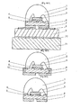
- Fig. 1 a first embodiment of an LED light source according to the invention
- Fig. 2 a modification of the in Fig. 1 illustrated LED
- Fig. 3 another modification of the in Fig.1 illustrated LED.
- an LED die 3 (R th, LED die ) is applied to a contact surface (eg, trace 5) of an LED PCB 6 (R th, LED PCB ) by means of a die adhesive 4 (R th, the die adhesive ) ,
- the LED Die 3 in Fig. 1 is mounted face-up and connected via bond wires 2 with the contact surfaces (trace 5).
- this can also be arranged in a face down mounting directly on the LED PCB 6 or this be mounted on a die-carrier face down, and the latter can then be arranged on the LED PCB.
- this arrangement is a separate LED lamp.
- this LED lamp by means of a placement technique (eg SMT) on a board 9 (R th, circuit board ), which is then optionally connected to a heat sink 11, for example via a soldering surface 10 (R th, LötFläche ).
- a placement technique eg SMT
- R th circuit board
- R th soldering surface 10
- the LED die 3 is usually cast in a material 1 with corresponding optical properties.
- the LED die can also - as is known - be used in a reflector. Of course, several LED dies can be cast together or used in a reflector.
- soldering properties of the LED array both manual soldering and in an automatic system (SMT wave or reflow soldering) can be improved by better Lotangriff and better thermal distribution. Furthermore, the solder joint is better to judge from the outside.
- the LED die 3 is not placed on a track 5, but directly on the core of the LED PCB 6. This is particularly true for metal core boards makes sense, because here between the interconnects 5 and the metal core, a thin insulating layer is necessary to electrically isolate the interconnects 5. This insulating layer also increases the thermal resistance, so that the direct placement of the LED dies 3 on the metal core of the LED PCB 6 has a smaller thermal resistance.
- the thermal resistances of the individual components should be kept as low as possible.
- solder contact layers with thermal conductivity above 20 W / mK and a layer thickness below 30 ⁇ m
- the ceramic has a ceramic substrate with thin film or thick film metallization.
- a ceramic substrate with thin film or thick film metallization.
- AlN or BN are used, or AlO is used in very thin layers.
- Metler core boards consist e.g. made of Cu or A1. These are provided with nonconductive layers, and then there are arranged conductor tracks (either galvanically or by coating by means of an adhesive / welding method).
- the insulating layer may consist of either organic materials or thin ceramics (the latter being, for example, clipped onto the metal substrate or coated with baked ceramic tapes).
- the thermal resistance of the arrangement it is preferable to use as thin as possible non-conductive layers (thinner than 50 ⁇ m). This is basically possible in LED applications, since LEDs are typically operated with a DC voltage of a few volts, so that no high breakdown field strengths occur. However, when handling the circuit board, it may too electrical discharges come.
- the insulator layers of the metal core board are designed to be electrically non-linear in such a way that they electrically insulate at low voltages (eg below 100 V), while they are electrically high at high voltages (eg above 100 V) become conductive. Such electrically non-linear materials are known in the art.
- the LED die can be placed directly on the metal core ( Fig. 3 ). Here, the lowest thermal resistances are achieved, and you can easily run the insulator layers thick.
- This can e.g. by arranging outwardly insulating metal cylinders which can be contacted from above and below.
- the thermal conductivity of the carrier material of an organic PCB is very poor (only 0.1-0.2 W / mK).
- metallization layer thicknesses of more than 100 ⁇ m, preferably more than 200 ⁇ m are necessary.
- these channels have a diameter of a few tenths of a mm. In an optimized variant, the diameter of the channels is only a few microns or nanometers. In this way, a substrate with very high anisotropic electrical and thermal conductivity is realized.
Landscapes
- Led Device Packages (AREA)
- Non-Portable Lighting Devices Or Systems Thereof (AREA)
- Led Devices (AREA)
- Illuminated Signs And Luminous Advertising (AREA)
Applications Claiming Priority (3)
| Application Number | Priority Date | Filing Date | Title |
|---|---|---|---|
| AT0107203A AT501081B8 (de) | 2003-07-11 | 2003-07-11 | Led sowie led-lichtquelle |
| EP04741760.5A EP1839344B1 (fr) | 2003-07-11 | 2004-06-09 | Diode électroluminescente et source de lumière à del |
| PCT/EP2004/051066 WO2005008790A2 (fr) | 2003-07-11 | 2004-06-09 | Del et source de lumière à del |
Related Parent Applications (3)
| Application Number | Title | Priority Date | Filing Date |
|---|---|---|---|
| EP04741760.5 Division | 2004-06-09 | ||
| EP04741760.5A Division EP1839344B1 (fr) | 2003-07-11 | 2004-06-09 | Diode électroluminescente et source de lumière à del |
| EP04741760.5A Division-Into EP1839344B1 (fr) | 2003-07-11 | 2004-06-09 | Diode électroluminescente et source de lumière à del |
Publications (3)
| Publication Number | Publication Date |
|---|---|
| EP2398080A2 true EP2398080A2 (fr) | 2011-12-21 |
| EP2398080A3 EP2398080A3 (fr) | 2014-04-23 |
| EP2398080B1 EP2398080B1 (fr) | 2019-08-14 |
Family
ID=34069593
Family Applications (2)
| Application Number | Title | Priority Date | Filing Date |
|---|---|---|---|
| EP04741760.5A Expired - Lifetime EP1839344B1 (fr) | 2003-07-11 | 2004-06-09 | Diode électroluminescente et source de lumière à del |
| EP11181590.8A Expired - Lifetime EP2398080B1 (fr) | 2003-07-11 | 2004-06-09 | Source lumineuse à diode électroluminescente |
Family Applications Before (1)
| Application Number | Title | Priority Date | Filing Date |
|---|---|---|---|
| EP04741760.5A Expired - Lifetime EP1839344B1 (fr) | 2003-07-11 | 2004-06-09 | Diode électroluminescente et source de lumière à del |
Country Status (5)
| Country | Link |
|---|---|
| US (1) | US8614456B2 (fr) |
| EP (2) | EP1839344B1 (fr) |
| AT (1) | AT501081B8 (fr) |
| CA (1) | CA2553921C (fr) |
| WO (1) | WO2005008790A2 (fr) |
Families Citing this family (8)
| Publication number | Priority date | Publication date | Assignee | Title |
|---|---|---|---|---|
| DE602005016280D1 (de) * | 2005-11-29 | 2009-10-08 | Nat Central University Jungli | Licht aussendendes Bauelement |
| CN100459194C (zh) * | 2006-02-28 | 2009-02-04 | 财团法人工业技术研究院 | 封装结构与封装方法 |
| US7735738B2 (en) | 2007-06-28 | 2010-06-15 | Symbol Technologies, Inc. | Thermal management in imaging reader |
| KR100877881B1 (ko) * | 2007-09-06 | 2009-01-08 | 엘지이노텍 주식회사 | 발광다이오드 패키지 및 그 제조방법 |
| US10256385B2 (en) * | 2007-10-31 | 2019-04-09 | Cree, Inc. | Light emitting die (LED) packages and related methods |
| US20100027281A1 (en) * | 2008-07-31 | 2010-02-04 | Waters Stanley E | LED Anti-Collision Light for Commercial Aircraft |
| WO2015101420A1 (fr) * | 2014-01-02 | 2015-07-09 | Tyco Electronics Nederland B.V. | Ensemble douille de del |
| US10908351B2 (en) | 2017-02-13 | 2021-02-02 | Signify Holding B.V. | Frame for supporting a light guide panel and luminaire comprising the frame |
Family Cites Families (48)
| Publication number | Priority date | Publication date | Assignee | Title |
|---|---|---|---|---|
| JPS6072281A (ja) | 1983-09-28 | 1985-04-24 | Sanyo Electric Co Ltd | 発光ダイオ−ド基板 |
| JPH0343750U (fr) * | 1989-09-04 | 1991-04-24 | ||
| US5491362A (en) * | 1992-04-30 | 1996-02-13 | Vlsi Technology, Inc. | Package structure having accessible chip |
| JP2915706B2 (ja) | 1992-07-15 | 1999-07-05 | シャープ株式会社 | 発光装置 |
| JPH06163794A (ja) * | 1992-11-19 | 1994-06-10 | Shinko Electric Ind Co Ltd | メタルコアタイプの多層リードフレーム |
| JP3535602B2 (ja) | 1995-03-23 | 2004-06-07 | 松下電器産業株式会社 | 面実装型led |
| JP3269397B2 (ja) * | 1995-09-19 | 2002-03-25 | 株式会社デンソー | プリント配線基板 |
| US6045240A (en) * | 1996-06-27 | 2000-04-04 | Relume Corporation | LED lamp assembly with means to conduct heat away from the LEDS |
| JPH11168235A (ja) | 1997-12-05 | 1999-06-22 | Toyoda Gosei Co Ltd | 発光ダイオード |
| JP3183643B2 (ja) | 1998-06-17 | 2001-07-09 | 株式会社カツラヤマテクノロジー | 凹みプリント配線板の製造方法 |
| AT407977B (de) * | 1999-03-02 | 2001-07-25 | Lumitech Univ Prof Dr Leising | Warndreieck mit roten reflektoren und innerhalb liegenden rot lumieszierenden flächen |
| DE19928576C2 (de) * | 1999-06-22 | 2003-05-22 | Osram Opto Semiconductors Gmbh | Oberflächenmontierbares LED-Bauelement mit verbesserter Wärmeabfuhr |
| DE19963264B4 (de) * | 1999-12-17 | 2007-05-31 | Optotransmitter-Umweltschutz-Technologie E.V. | Trägermaterial für elektronische Hochleistungs-Bauelemente in SMD-Bauform und ein damit hergestelltes elektronisches Hochleistungs-Bauelement |
| TW465123B (en) * | 2000-02-02 | 2001-11-21 | Ind Tech Res Inst | High power white light LED |
| US6428189B1 (en) * | 2000-03-31 | 2002-08-06 | Relume Corporation | L.E.D. thermal management |
| JP2001345485A (ja) * | 2000-06-02 | 2001-12-14 | Toyoda Gosei Co Ltd | 発光装置 |
| US6452217B1 (en) * | 2000-06-30 | 2002-09-17 | General Electric Company | High power LED lamp structure using phase change cooling enhancements for LED lighting products |
| DE10033502A1 (de) * | 2000-07-10 | 2002-01-31 | Osram Opto Semiconductors Gmbh | Optoelektronisches Modul, Verfahren zu dessen Herstellung und dessen Verwendung |
| AT413062B (de) * | 2000-07-12 | 2005-10-15 | Tridonic Optoelectronics Gmbh | Verfahren zur herstellung einer led-lichtquelle |
| TW459403B (en) * | 2000-07-28 | 2001-10-11 | Lee Jeong Hoon | White light-emitting diode |
| US6614103B1 (en) * | 2000-09-01 | 2003-09-02 | General Electric Company | Plastic packaging of LED arrays |
| US6345903B1 (en) * | 2000-09-01 | 2002-02-12 | Citizen Electronics Co., Ltd. | Surface-mount type emitting diode and method of manufacturing same |
| JP4077170B2 (ja) * | 2000-09-21 | 2008-04-16 | シャープ株式会社 | 半導体発光装置 |
| US6867493B2 (en) * | 2000-11-15 | 2005-03-15 | Skyworks Solutions, Inc. | Structure and method for fabrication of a leadless multi-die carrier |
| JP5110744B2 (ja) * | 2000-12-21 | 2012-12-26 | フィリップス ルミレッズ ライティング カンパニー リミテッド ライアビリティ カンパニー | 発光装置及びその製造方法 |
| MY145695A (en) * | 2001-01-24 | 2012-03-30 | Nichia Corp | Light emitting diode, optical semiconductor device, epoxy resin composition suited for optical semiconductor device, and method for manufacturing the same |
| US6639360B2 (en) * | 2001-01-31 | 2003-10-28 | Gentex Corporation | High power radiation emitter device and heat dissipating package for electronic components |
| US7075112B2 (en) * | 2001-01-31 | 2006-07-11 | Gentex Corporation | High power radiation emitter device and heat dissipating package for electronic components |
| JP2003115204A (ja) | 2001-10-04 | 2003-04-18 | Toyoda Gosei Co Ltd | 遮光反射型デバイス及び光源 |
| US6833566B2 (en) * | 2001-03-28 | 2004-12-21 | Toyoda Gosei Co., Ltd. | Light emitting diode with heat sink |
| JP2002299698A (ja) * | 2001-03-30 | 2002-10-11 | Sumitomo Electric Ind Ltd | 発光装置 |
| WO2002090826A1 (fr) * | 2001-05-08 | 2002-11-14 | Lumileds Lighting The Netherlands B.V. | Systeme d'eclairage et dispositif d'affichage |
| KR100419611B1 (ko) * | 2001-05-24 | 2004-02-25 | 삼성전기주식회사 | 발광다이오드 및 이를 이용한 발광장치와 그 제조방법 |
| JP4813691B2 (ja) * | 2001-06-06 | 2011-11-09 | シチズン電子株式会社 | 発光ダイオード |
| JP4959071B2 (ja) * | 2001-07-04 | 2012-06-20 | ローム株式会社 | 面実装型半導体装置 |
| TW543128B (en) * | 2001-07-12 | 2003-07-21 | Highlink Technology Corp | Surface mounted and flip chip type LED package |
| US6670648B2 (en) * | 2001-07-19 | 2003-12-30 | Rohm Co., Ltd. | Semiconductor light-emitting device having a reflective case |
| CN1464953A (zh) * | 2001-08-09 | 2003-12-31 | 松下电器产业株式会社 | Led照明装置和卡型led照明光源 |
| US6498355B1 (en) * | 2001-10-09 | 2002-12-24 | Lumileds Lighting, U.S., Llc | High flux LED array |
| US6531328B1 (en) * | 2001-10-11 | 2003-03-11 | Solidlite Corporation | Packaging of light-emitting diode |
| US6827468B2 (en) * | 2001-12-10 | 2004-12-07 | Robert D. Galli | LED lighting assembly |
| US6599768B1 (en) * | 2002-08-20 | 2003-07-29 | United Epitaxy Co., Ltd. | Surface mounting method for high power light emitting diode |
| US7800121B2 (en) * | 2002-08-30 | 2010-09-21 | Lumination Llc | Light emitting diode component |
| US7244965B2 (en) * | 2002-09-04 | 2007-07-17 | Cree Inc, | Power surface mount light emitting die package |
| TW578280B (en) * | 2002-11-21 | 2004-03-01 | United Epitaxy Co Ltd | Light emitting diode and package scheme and method thereof |
| US20040188696A1 (en) * | 2003-03-28 | 2004-09-30 | Gelcore, Llc | LED power package |
| KR20040092512A (ko) * | 2003-04-24 | 2004-11-04 | (주)그래픽테크노재팬 | 방열 기능을 갖는 반사판이 구비된 반도체 발광장치 |
| US6876008B2 (en) * | 2003-07-31 | 2005-04-05 | Lumileds Lighting U.S., Llc | Mount for semiconductor light emitting device |
-
2003
- 2003-07-11 AT AT0107203A patent/AT501081B8/de not_active IP Right Cessation
-
2004
- 2004-06-09 CA CA2553921A patent/CA2553921C/fr not_active Expired - Fee Related
- 2004-06-09 WO PCT/EP2004/051066 patent/WO2005008790A2/fr not_active Ceased
- 2004-06-09 US US10/586,386 patent/US8614456B2/en not_active Expired - Fee Related
- 2004-06-09 EP EP04741760.5A patent/EP1839344B1/fr not_active Expired - Lifetime
- 2004-06-09 EP EP11181590.8A patent/EP2398080B1/fr not_active Expired - Lifetime
Non-Patent Citations (1)
| Title |
|---|
| None |
Also Published As
| Publication number | Publication date |
|---|---|
| AT501081B1 (de) | 2006-06-15 |
| US20070111351A1 (en) | 2007-05-17 |
| EP2398080A3 (fr) | 2014-04-23 |
| CA2553921A1 (fr) | 2005-01-27 |
| EP2398080B1 (fr) | 2019-08-14 |
| EP1839344B1 (fr) | 2017-03-01 |
| WO2005008790A3 (fr) | 2005-06-09 |
| CA2553921C (fr) | 2014-03-18 |
| EP1839344A2 (fr) | 2007-10-03 |
| US8614456B2 (en) | 2013-12-24 |
| AT501081B8 (de) | 2007-02-15 |
| WO2005008790A2 (fr) | 2005-01-27 |
| AT501081A4 (de) | 2006-06-15 |
Similar Documents
| Publication | Publication Date | Title |
|---|---|---|
| DE10351934B4 (de) | Leuchtdioden-Anordnung mit wärmeabführender Platine | |
| EP2397754B1 (fr) | Corps de support pour composants ou circuits | |
| DE102008048005B3 (de) | Leistungshalbleitermodulanordnung und Verfahren zur Herstellung einer Leistungshalbleitermodulanordnung | |
| DE19939933A1 (de) | Leistungs-Moduleinheit | |
| EP1411549A1 (fr) | Module semiconducteur de puissance avec des nanotubes de carbone conducteurs d'électricité | |
| EP1445799B1 (fr) | Dispositif à dissipation de chaleur pour un semi-conducteur sur un circuit imprimé | |
| DE102008012256A1 (de) | Elektronik-Komponenten-Montageplatte | |
| EP2398080B1 (fr) | Source lumineuse à diode électroluminescente | |
| EP1455391B1 (fr) | Module semiconducteur de puissance avec composant de détection | |
| AT515440B1 (de) | Elektrische Bauteilanordnung | |
| DE102014107217A1 (de) | Leistungshalbleitermodul | |
| DE102019116021B4 (de) | Flexible Leiterplatte mit thermisch leitender Verbindung zu einer Wärmesenke | |
| DE102014203310A1 (de) | Elektronikmodul | |
| DE10121969C1 (de) | Schaltungsanordnung in Druckkontaktierung und Verfahren zu seiner Herstellung | |
| EP2033219A1 (fr) | Boîtier de puissance pour puces à semi-conducteur et configuration dudit boîtier pour la dissipation de chaleur | |
| DE102004035746B4 (de) | Leistungshalbleitermodul | |
| WO2017032613A1 (fr) | Composant électroluminescent | |
| DE202014002028U1 (de) | Elektrische Bauteilanordnung | |
| AT6437U1 (de) | Elektrische schaltung | |
| EP3059760A1 (fr) | Dispositif électronique |
Legal Events
| Date | Code | Title | Description |
|---|---|---|---|
| AC | Divisional application: reference to earlier application |
Ref document number: 1839344 Country of ref document: EP Kind code of ref document: P |
|
| AK | Designated contracting states |
Kind code of ref document: A2 Designated state(s): AT BE BG CH CY CZ DE DK EE ES FI FR GB GR HU IE IT LI LU MC NL PL PT RO SE SI SK TR |
|
| AX | Request for extension of the european patent |
Extension state: AL HR LT LV MK |
|
| PUAI | Public reference made under article 153(3) epc to a published international application that has entered the european phase |
Free format text: ORIGINAL CODE: 0009012 |
|
| PUAL | Search report despatched |
Free format text: ORIGINAL CODE: 0009013 |
|
| AK | Designated contracting states |
Kind code of ref document: A3 Designated state(s): AT BE BG CH CY CZ DE DK EE ES FI FR GB GR HU IE IT LI LU MC NL PL PT RO SE SI SK TR |
|
| AX | Request for extension of the european patent |
Extension state: AL HR LT LV MK |
|
| RIC1 | Information provided on ipc code assigned before grant |
Ipc: H01L 33/48 20100101AFI20140319BHEP |
|
| 17P | Request for examination filed |
Effective date: 20141023 |
|
| RBV | Designated contracting states (corrected) |
Designated state(s): AT BE BG CH CY CZ DE DK EE ES FI FR GB GR HU IE IT LI LU MC NL PL PT RO SE SI SK TR |
|
| STAA | Information on the status of an ep patent application or granted ep patent |
Free format text: STATUS: EXAMINATION IS IN PROGRESS |
|
| 17Q | First examination report despatched |
Effective date: 20170220 |
|
| GRAP | Despatch of communication of intention to grant a patent |
Free format text: ORIGINAL CODE: EPIDOSNIGR1 |
|
| STAA | Information on the status of an ep patent application or granted ep patent |
Free format text: STATUS: GRANT OF PATENT IS INTENDED |
|
| INTG | Intention to grant announced |
Effective date: 20190607 |
|
| GRAS | Grant fee paid |
Free format text: ORIGINAL CODE: EPIDOSNIGR3 |
|
| GRAA | (expected) grant |
Free format text: ORIGINAL CODE: 0009210 |
|
| STAA | Information on the status of an ep patent application or granted ep patent |
Free format text: STATUS: THE PATENT HAS BEEN GRANTED |
|
| AC | Divisional application: reference to earlier application |
Ref document number: 1839344 Country of ref document: EP Kind code of ref document: P |
|
| AK | Designated contracting states |
Kind code of ref document: B1 Designated state(s): AT BE BG CH CY CZ DE DK EE ES FI FR GB GR HU IE IT LI LU MC NL PL PT RO SE SI SK TR |
|
| REG | Reference to a national code |
Ref country code: GB Ref legal event code: FG4D Free format text: NOT ENGLISH |
|
| REG | Reference to a national code |
Ref country code: CH Ref legal event code: EP Ref country code: AT Ref legal event code: REF Ref document number: 1168062 Country of ref document: AT Kind code of ref document: T Effective date: 20190815 |
|
| REG | Reference to a national code |
Ref country code: IE Ref legal event code: FG4D Free format text: LANGUAGE OF EP DOCUMENT: GERMAN |
|
| REG | Reference to a national code |
Ref country code: DE Ref legal event code: R096 Ref document number: 502004015822 Country of ref document: DE |
|
| REG | Reference to a national code |
Ref country code: NL Ref legal event code: MP Effective date: 20190814 |
|
| PG25 | Lapsed in a contracting state [announced via postgrant information from national office to epo] |
Ref country code: NL Free format text: LAPSE BECAUSE OF FAILURE TO SUBMIT A TRANSLATION OF THE DESCRIPTION OR TO PAY THE FEE WITHIN THE PRESCRIBED TIME-LIMIT Effective date: 20190814 Ref country code: FI Free format text: LAPSE BECAUSE OF FAILURE TO SUBMIT A TRANSLATION OF THE DESCRIPTION OR TO PAY THE FEE WITHIN THE PRESCRIBED TIME-LIMIT Effective date: 20190814 Ref country code: SE Free format text: LAPSE BECAUSE OF FAILURE TO SUBMIT A TRANSLATION OF THE DESCRIPTION OR TO PAY THE FEE WITHIN THE PRESCRIBED TIME-LIMIT Effective date: 20190814 Ref country code: PT Free format text: LAPSE BECAUSE OF FAILURE TO SUBMIT A TRANSLATION OF THE DESCRIPTION OR TO PAY THE FEE WITHIN THE PRESCRIBED TIME-LIMIT Effective date: 20191216 Ref country code: BG Free format text: LAPSE BECAUSE OF FAILURE TO SUBMIT A TRANSLATION OF THE DESCRIPTION OR TO PAY THE FEE WITHIN THE PRESCRIBED TIME-LIMIT Effective date: 20191114 |
|
| PG25 | Lapsed in a contracting state [announced via postgrant information from national office to epo] |
Ref country code: ES Free format text: LAPSE BECAUSE OF FAILURE TO SUBMIT A TRANSLATION OF THE DESCRIPTION OR TO PAY THE FEE WITHIN THE PRESCRIBED TIME-LIMIT Effective date: 20190814 Ref country code: GR Free format text: LAPSE BECAUSE OF FAILURE TO SUBMIT A TRANSLATION OF THE DESCRIPTION OR TO PAY THE FEE WITHIN THE PRESCRIBED TIME-LIMIT Effective date: 20191115 |
|
| PG25 | Lapsed in a contracting state [announced via postgrant information from national office to epo] |
Ref country code: TR Free format text: LAPSE BECAUSE OF FAILURE TO SUBMIT A TRANSLATION OF THE DESCRIPTION OR TO PAY THE FEE WITHIN THE PRESCRIBED TIME-LIMIT Effective date: 20190814 |
|
| PG25 | Lapsed in a contracting state [announced via postgrant information from national office to epo] |
Ref country code: DK Free format text: LAPSE BECAUSE OF FAILURE TO SUBMIT A TRANSLATION OF THE DESCRIPTION OR TO PAY THE FEE WITHIN THE PRESCRIBED TIME-LIMIT Effective date: 20190814 Ref country code: PL Free format text: LAPSE BECAUSE OF FAILURE TO SUBMIT A TRANSLATION OF THE DESCRIPTION OR TO PAY THE FEE WITHIN THE PRESCRIBED TIME-LIMIT Effective date: 20190814 Ref country code: EE Free format text: LAPSE BECAUSE OF FAILURE TO SUBMIT A TRANSLATION OF THE DESCRIPTION OR TO PAY THE FEE WITHIN THE PRESCRIBED TIME-LIMIT Effective date: 20190814 Ref country code: RO Free format text: LAPSE BECAUSE OF FAILURE TO SUBMIT A TRANSLATION OF THE DESCRIPTION OR TO PAY THE FEE WITHIN THE PRESCRIBED TIME-LIMIT Effective date: 20190814 Ref country code: IT Free format text: LAPSE BECAUSE OF FAILURE TO SUBMIT A TRANSLATION OF THE DESCRIPTION OR TO PAY THE FEE WITHIN THE PRESCRIBED TIME-LIMIT Effective date: 20190814 |
|
| REG | Reference to a national code |
Ref country code: DE Ref legal event code: R084 Ref document number: 502004015822 Country of ref document: DE |
|
| PG25 | Lapsed in a contracting state [announced via postgrant information from national office to epo] |
Ref country code: CZ Free format text: LAPSE BECAUSE OF FAILURE TO SUBMIT A TRANSLATION OF THE DESCRIPTION OR TO PAY THE FEE WITHIN THE PRESCRIBED TIME-LIMIT Effective date: 20190814 Ref country code: SK Free format text: LAPSE BECAUSE OF FAILURE TO SUBMIT A TRANSLATION OF THE DESCRIPTION OR TO PAY THE FEE WITHIN THE PRESCRIBED TIME-LIMIT Effective date: 20190814 |
|
| REG | Reference to a national code |
Ref country code: DE Ref legal event code: R097 Ref document number: 502004015822 Country of ref document: DE |
|
| PLBE | No opposition filed within time limit |
Free format text: ORIGINAL CODE: 0009261 |
|
| STAA | Information on the status of an ep patent application or granted ep patent |
Free format text: STATUS: NO OPPOSITION FILED WITHIN TIME LIMIT |
|
| 26N | No opposition filed |
Effective date: 20200603 |
|
| PG25 | Lapsed in a contracting state [announced via postgrant information from national office to epo] |
Ref country code: SI Free format text: LAPSE BECAUSE OF FAILURE TO SUBMIT A TRANSLATION OF THE DESCRIPTION OR TO PAY THE FEE WITHIN THE PRESCRIBED TIME-LIMIT Effective date: 20190814 |
|
| PG25 | Lapsed in a contracting state [announced via postgrant information from national office to epo] |
Ref country code: MC Free format text: LAPSE BECAUSE OF FAILURE TO SUBMIT A TRANSLATION OF THE DESCRIPTION OR TO PAY THE FEE WITHIN THE PRESCRIBED TIME-LIMIT Effective date: 20190814 |
|
| REG | Reference to a national code |
Ref country code: CH Ref legal event code: PL |
|
| PG25 | Lapsed in a contracting state [announced via postgrant information from national office to epo] |
Ref country code: LU Free format text: LAPSE BECAUSE OF NON-PAYMENT OF DUE FEES Effective date: 20200609 |
|
| REG | Reference to a national code |
Ref country code: BE Ref legal event code: MM Effective date: 20200630 |
|
| PG25 | Lapsed in a contracting state [announced via postgrant information from national office to epo] |
Ref country code: LI Free format text: LAPSE BECAUSE OF NON-PAYMENT OF DUE FEES Effective date: 20200630 Ref country code: IE Free format text: LAPSE BECAUSE OF NON-PAYMENT OF DUE FEES Effective date: 20200609 Ref country code: CH Free format text: LAPSE BECAUSE OF NON-PAYMENT OF DUE FEES Effective date: 20200630 Ref country code: FR Free format text: LAPSE BECAUSE OF NON-PAYMENT OF DUE FEES Effective date: 20200630 |
|
| PG25 | Lapsed in a contracting state [announced via postgrant information from national office to epo] |
Ref country code: BE Free format text: LAPSE BECAUSE OF NON-PAYMENT OF DUE FEES Effective date: 20200630 |
|
| REG | Reference to a national code |
Ref country code: AT Ref legal event code: MM01 Ref document number: 1168062 Country of ref document: AT Kind code of ref document: T Effective date: 20200609 |
|
| PGFP | Annual fee paid to national office [announced via postgrant information from national office to epo] |
Ref country code: GB Payment date: 20210625 Year of fee payment: 18 |
|
| PG25 | Lapsed in a contracting state [announced via postgrant information from national office to epo] |
Ref country code: AT Free format text: LAPSE BECAUSE OF NON-PAYMENT OF DUE FEES Effective date: 20200609 |
|
| REG | Reference to a national code |
Ref country code: DE Ref legal event code: R081 Ref document number: 502004015822 Country of ref document: DE Owner name: TRIDONIC GMBH & CO KG, AT Free format text: FORMER OWNER: TRIDONIC JENNERSDORF GMBH, JENNERSDORF, AT |
|
| PG25 | Lapsed in a contracting state [announced via postgrant information from national office to epo] |
Ref country code: CY Free format text: LAPSE BECAUSE OF FAILURE TO SUBMIT A TRANSLATION OF THE DESCRIPTION OR TO PAY THE FEE WITHIN THE PRESCRIBED TIME-LIMIT Effective date: 20190814 |
|
| PGFP | Annual fee paid to national office [announced via postgrant information from national office to epo] |
Ref country code: DE Payment date: 20220628 Year of fee payment: 19 |
|
| GBPC | Gb: european patent ceased through non-payment of renewal fee |
Effective date: 20220609 |
|
| PG25 | Lapsed in a contracting state [announced via postgrant information from national office to epo] |
Ref country code: GB Free format text: LAPSE BECAUSE OF NON-PAYMENT OF DUE FEES Effective date: 20220609 |
|
| REG | Reference to a national code |
Ref country code: DE Ref legal event code: R119 Ref document number: 502004015822 Country of ref document: DE |
|
| PG25 | Lapsed in a contracting state [announced via postgrant information from national office to epo] |
Ref country code: DE Free format text: LAPSE BECAUSE OF NON-PAYMENT OF DUE FEES Effective date: 20240103 |