EP2704178B1 - Imagerie d'un échantillon dans un TEM équipé d'une plaque de phase - Google Patents
Imagerie d'un échantillon dans un TEM équipé d'une plaque de phase Download PDFInfo
- Publication number
- EP2704178B1 EP2704178B1 EP12182334.8A EP12182334A EP2704178B1 EP 2704178 B1 EP2704178 B1 EP 2704178B1 EP 12182334 A EP12182334 A EP 12182334A EP 2704178 B1 EP2704178 B1 EP 2704178B1
- Authority
- EP
- European Patent Office
- Prior art keywords
- enhancing device
- image
- electrons
- contrast enhancing
- sample
- Prior art date
- Legal status (The legal status is an assumption and is not a legal conclusion. Google has not performed a legal analysis and makes no representation as to the accuracy of the status listed.)
- Active
Links
Images


Classifications
-
- H—ELECTRICITY
- H01—ELECTRIC ELEMENTS
- H01J—ELECTRIC DISCHARGE TUBES OR DISCHARGE LAMPS
- H01J31/00—Cathode ray tubes; Electron beam tubes
- H01J31/08—Cathode ray tubes; Electron beam tubes having a screen on or from which an image or pattern is formed, picked up, converted, or stored
- H01J31/26—Image pick-up tubes having an input of visible light and electric output
- H01J31/28—Image pick-up tubes having an input of visible light and electric output with electron ray scanning the image screen
- H01J31/283—Image pick-up tubes having an input of visible light and electric output with electron ray scanning the image screen with a target comprising semiconductor junctions
-
- H—ELECTRICITY
- H01—ELECTRIC ELEMENTS
- H01J—ELECTRIC DISCHARGE TUBES OR DISCHARGE LAMPS
- H01J37/00—Discharge tubes with provision for introducing objects or material to be exposed to the discharge, e.g. for the purpose of examination or processing thereof
- H01J37/26—Electron or ion microscopes; Electron or ion diffraction tubes
-
- H—ELECTRICITY
- H01—ELECTRIC ELEMENTS
- H01J—ELECTRIC DISCHARGE TUBES OR DISCHARGE LAMPS
- H01J37/00—Discharge tubes with provision for introducing objects or material to be exposed to the discharge, e.g. for the purpose of examination or processing thereof
- H01J37/26—Electron or ion microscopes; Electron or ion diffraction tubes
- H01J37/261—Details
- H01J37/263—Contrast, resolution or power of penetration
-
- H—ELECTRICITY
- H01—ELECTRIC ELEMENTS
- H01J—ELECTRIC DISCHARGE TUBES OR DISCHARGE LAMPS
- H01J2237/00—Discharge tubes exposing object to beam, e.g. for analysis treatment, etching, imaging
- H01J2237/26—Electron or ion microscopes
- H01J2237/2614—Holography or phase contrast, phase related imaging in general, e.g. phase plates
Definitions
- the invention relates to a method of forming an image of a sample in a transmission electron microscope, the sample irradiated by a beam of electrons and the sample splitting the beam of electrons in a beam of undiffracted (non-scattered) electrons and beams of diffracted (scattered) electrons, the electron microscope equipped with a contrast enhancing device from the group of phase plates, Foucault device or Hilbert device, the contrast enhancing device for improving the contrast at low spatial frequencies, the contrast enhancing device positioned in the back focal plane of the objective lens or in an image of said plane, the contrast enhancing device showing a position with respect to the beam of unscattered electrons.
- TEM Transmission Electron Microscope
- contrast mechanisms also contribute to the image, such as the local absence of electrons that are locally absorbed in the sample, or electrons that are absorbed by the contrast enhancing device
- Especially biological samples comprising mainly low-Z materials, show weak phase images.
- the contrast is a function of the spatial frequency, and especially at low spatial frequencies the contrast is low. This is described by the Contrast Transfer Function (CTF) as shown in Nagayama [-1-], more specifically figure 2 .
- CTF Contrast Transfer Function
- phase plate can be introduced in the back-focal plane of the objective lens, also known as the diffraction plane.
- the back-focal plane of the objective lens is a Fourier representation of the image, and at this plane the angle under which electrons are scattered results in different positions in this plane.
- this plane it is possible to introduce, for example, a phase shift of - ⁇ /2 to all electrons except the unscattered beam. Interference of the now phase shifted scattered beam with the non-phase shifted undiffracted electrons results in a much higher CTF, as shown in aforementioned figure 2 of Nagayama [-1-].
- Nagayama [-1-] describes several contrast enhancing devices to be used in the diffraction plane.
- this is a thin film with a thickness causing a phase shift of approximately - ⁇ /2 for the electrons passing through it. It is a carbon film, and almost all electrons pass through it without absorption or scattering. In the center of the film a small hole is formed for passing the beam of unscattered electrons. As a result a phase shift of ⁇ /2 between scattered and unscattered electrons is caused, and the phase variation is changed to an amplitude variation (the sine like CTF is changed to a cosine like CTF).
- phase plate shows artifacts in the form of "ringing”: due to the abrupt edge of the phase plate a sudden transition in the Fourier domain from 0 ⁇ - ⁇ /2 is introduced, resulting in ripples in the normal image plane. This is explained in more detail in “ Optimizing the phase shift and the cut-on periodicity of phase plates for TEM", R. Danev et al., Ultramicroscopy 111 (2011) pages 1305-1315 , further referred to as Danev [-2-].
- phase plate Another disadvantage of said phase plate is that small irregularities of the thin film, or of small dust motes thereupon, cause local disturbance of the phase.
- the hole needs to be a very small hole, as all electrons passing through the hole have the same phase shift, and thus all these electrons show little contrast.
- the hole diameter determines the acceptance angle of electrons passing through it, and thus the spatial frequency at which contrast enhancement starts.
- the invention intends to provide a solution to the above mentioned problems.
- the method according to the invention is characterized in that during the formation of the image the mutual position of the contrast enhancing device and the beam of unscattered electrons is changed.
- the contrast enhancing device for example the phase plate
- the beam of unscattered electrons and the rest of the diffraction pattern, as the contrast enhancing device is placed in the diffraction plane
- the sudden transition in the Fourier domain due to the edge discontinuity is blurred, effectively forming a gradual transition.
- the ringing is strongly suppressed.
- the mutual movement takes the form of a circular movement of the contrast enhancing device relative to the undiffracted electrons which is fast compared to the image acquisition time.
- a movement of between 1 and 50 revolutions per second, more specifically between 5 - 20 revolutions per second is proposed.
- such a contrast enhancing device is also called an orbiting mode contrast enhancing device (e.g. orbiting mode phase plate).
- the amplitude of the movement should be such that the undiffracted beam always passes through the hole, so the diameter of the circular movement should be less than the diameter of the hole and the circular movement should be concentric with the hole perimeter.
- phase plate according to the invention the diameter of the hole need not be as small as for the phase plate used in the conventional method: for all electrons passing at a distance larger than the smallest distance from the undiffracted beam to the edge of the hole at least a part of the electrons passes through the thin film, thus experiencing a phase shift with the associated improvement in contrast.
- the electron transparency of the thin film is large, a part of the electrons are intercepted.
- the centering of the beam with respect to the hole in the thin film can be measured.
- centering of the contrast enhancing device with respect to the beam is achieved.
- the measuring capability also enables matching the (fixed) diameter of the hole and the (variable) diameter of the circular movement.
- the signal can also be used to minimize ellipticity of the assumed circular movement, analog to the method mentioned in EP publication No. EP2485240A1 . This is true when deflecting the beam in a circular fashion using electric or magnetic fields, or when mechanically moving the phase plate.
- Figure 1 schematically shows a TEM 100 equipped with a phase plate.
- Figure 1 shows a particle source 104 producing a beam of particles, such as electrons, along optical axis 102.
- the particles have a selectable energy of typically between 80 - 300 keV, although higher energies, e.g. 400 keV - 1 MeV, or lower energies, e.g. 50 keV, may be used.
- the beam of particles is manipulated by condenser system 106 to form a parallel beam impinging on a sample 108, the sample positioned with a sample holder 110.
- the sample holder can position the sample with respect to the optical axis and may shift the sample in the plane perpendicular to the optical axis and tilt the sample with respect to said axis.
- Objective lens 112 forms a magnified image of the sample.
- the objective lens is followed by a magnifying system 116, e.g. a doublet of lenses, forming an enlarged image of the back-focal plane 114 of the objective lens.
- a phase plate 118 is placed in the enlarged image of the back-focal plane of the objective lens, this conjugated plane positioned between the magnifying system and a projection system 122.
- the phase plate is positioned with a manipulator 120, allowing the phase plate to be centered round the optical axis.
- the projection system forms a magnified image of the sample on a detector 124, thereby revealing sample details of e.g. 0.1 nm.
- the detector may take the form of a fluorescent screen, or e.g. a CCD or CMOS camera.
- the screen can be viewed via the glass window 126.
- the TEM comprises a large number of deflectors, schematically shown as 128-1..128-7, although other deflectors on other places may be included.
- phase plate may also be positioned in the back-focal plane itself, in which case the magnifying system 116 is superfluous.
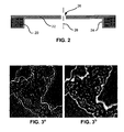
- Figure 2 schematically shows a Zernike phase plate.
- phase plate is discussed in e.g. Nagayama [-1-].
- the known phase plate comprises a holder structure 20 in the form of, for example, a standard platinum diaphragm with an aperture, as routinely used in electron microscopes.
- the outer diameter of such a standard platinum diaphragm is typically 3.05 mm, although other diameters are used.
- a thin foil 22 of amorphous carbon is placed on this holder structure.
- a thin foil 22 of amorphous carbon is placed on this holder structure.
- the carbon coating is typically made by vacuum evaporation, resulting in an additional amorphous carbon layer.
- the centre of the foil shows a through-hole 26 for passing the undiffracted beam.
- This hole 26 has a diameter sufficient to pass the undiffracted beam, but preferably not much more, as then slightly scattered electrons, corresponding with electrons scattered by large structures (low spatial frequencies) do not pass through the foil to get the required phase shift but instead through the central hole.
- the through-hole shows a diameter of less than 1 ⁇ m, formed in the foil using a focused ion beam.
- the phase plate preferably shows rotational symmetry around axis 28. It is noted that the undiffracted beam should also be well aligned round this axis 28.
- phase plate uses a round diaphragm as holder structure (support structure), but that also silicon structures (with a round or square inner or outer perimeter) are known to be used.
- silicon phase plate can be made using lithographic techniques, optionally combined with ion beam milling for forming the central through-hole in the thin film.
- carbon is used for the thin film of phase plates.
- other materials such as silicon may be used.
- Figure 3 a shows an image obtained in a microscope equipped with a phase plate.
- the image in the back-focal plane of the objective lens 112 also known as the diffraction plane, is equivalent to the object (sample) function in Fourier space.
- the phase plate 118 causes a phase shift for all electrons impinging and travelling through the film, and causes no phase shift for all electrons passing through the central hole.
- the phase plate causes a phase shift for all electrons scattered by structures with a spatial frequency above a threshold value, the threshold value given by the diameter of the hole, and causes no phase shift for electrons scattered by structures with a spatial frequency below said threshold value, or not scattered at all.
- Figure 3 b shows an image obtained with a TEM with orbital mode phase plate.
- the time-dependent position was realized by an orbital motion of the undiffracted beam relative to the phase plate by using a conical beam tilt at the sample with a period less than the integration time used to acquire an image at the image detector 124.
- a rotation frequency of approximately 10 Hz was used.
- the hole diameter was approximately 1 ⁇ m, and the orbital radius larger than 0.8 times the radius of the hole.
- the recording time of the image was more than one second.
- the orbital motion has the effect that the edge discontinuity caused by the phase plate is smeared out, thus smearing out the ripples in the image. Only a weak halo effect may remain, close to the strong-contrast features. Not only the rippling effect has largely disappeared, also the image can more easily be interpreted.
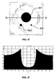
- Figure 4 a shows a simulated image of a sample imaged by a prior art phase plate with a central hole diameter of 1000 nm and a cut-on periodicity of 14.5 nm -1 .
- this simulation also described in Danev [-2-], paragraph 3, three modeled objects, object 401, with a diameter of 80 nm, object 402 with a diameter of 20 nm, and object 403 with a diameter of 10 nm are imaged.
- object 401 with a diameter of 80 nm
- object 402 with a diameter of 20 nm
- object 403 with a diameter of 10 nm
- Figure 4 b shows the intensity variations along line AA' of figure 4 a .
- the intensity is shown, ranging from 0 to 1.6, where 1 is the intensity far from the objects, and horizontally the position along line AA'. Round the largest diameter of object 401 (the edges) sharp maxima are visible. Also the ringing is quite discernable.
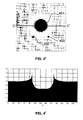
- Figure 4 c shows a similar image as figure 4 a , but now the central hole diameter of the phase plate is 100 nm and the cut-on periodicity is 145 nm -1 .
- Figure 4 d shows the intensity variations along line BB' of figure 4 c .
- the intensity is shown, ranging from 0 to 1.6, where 1 is the intensity far from the objects, and horizontally the position along line BB'. Round the largest diameter of object 401 (the edges) a large halo is discernable, as a result of which an intensity above 1 is found to a large distance from object 401.
- Figure 4 e shows a simulated image of a sample imaged by an "orbital mode" phase plate with a central hole diameter of 1000 nm, an orbital radius of 450 nm and an effective cut-on of 145 nm. This image shows less ringing and halo than either 4 a or 4 c .
- Figure 4 f shows the intensity variations along line CC' of figure 4 e . Vertically the intensity is shown, ranging from 0 to 1.6, where 1 is the intensity far from the objects, and horizontally the position along line CC'. Halo is much less pronounced than in figure 4 d (phase plate with a hole of 0.1 ⁇ m), and ringing is almost absent.
- the large hole size is a big manufacturing advantage, while centering and adjusting the size of the orbital motion is easily done with the deflectors that are present in a TEM. Therefore this orbital mode phase plate combines improved image quality with ease of manufacturing.
- phase enhancing devices are the Foucault knife contrast enhancing device, as described by e.g. Nagayama [-1-].
- a part of the diffracted electrons is blocked by a knife edge placed in the diffraction plane of the TEM, blocking one half-plane.
- Phase contrast now arises by the interference of the undiffracted central beam and the diffracted electrons of the half plane that is not blocked.
- a phase shift of ⁇ is introduced between the two half planes.
- Figure 5 shows a view of a Foucault knife.
- the device shows a blocking member 52 mounted on a holder structure 50, the blocking member blocking half the plane.
- the device is positioned such, that the undiffracted beam is just passing past the edge along line 54.
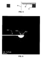
- Figure 6 schematically shows a variant of the Foucault knife.
- Figure 6 shows a diffraction pattern overlaid with a blocking member 602.
- the blocking member is connected to the holder structure (not shown) via support arm 604.
- the blocking member is positioned close to the undiffracted beam 600.
- the blocking member is here formed as a half-circle with a straight edge. In the centre of the circle an indent is formed where the undiffracted beam can pass, so that these electrons do not impinge on the blocking member.
- This indent ensures a low frequency behavior of the blocking member for a low frequency that is identical in all directions.
Landscapes
- Chemical & Material Sciences (AREA)
- Analytical Chemistry (AREA)
- Analysing Materials By The Use Of Radiation (AREA)
Claims (13)
- Procédé de formation d'une image d'un échantillon dans un microscope électronique à transmission, l'échantillon étant irradié par un faisceau d'électrons et l'échantillon séparant le faisceau d'électrons en un faisceau d'électrons non diffractés et des faisceaux d'électrons dispersés, le microscope électronique étant équipé d'un dispositif d'amélioration de contraste parmi le groupe des plaques de phase, des dispositifs de Foucault ou des dispositifs de Hilbert, le dispositif d'amélioration de contraste améliorant le contraste à des fréquences spatiales faibles, le dispositif d'amélioration de contraste étant positionné dans le plan focal arrière de l'objectif ou dans une image dudit plan, le dispositif d'amélioration de contraste montrant une position par rapport au faisceau d'électrons non dispersés,
le procédé étant caractérisé en ce que
pendant la formation de l'image, la position réciproque du dispositif d'amélioration de contraste et du faisceau d'électrons non dispersés est modifiée. - Procédé selon la revendication 1, dans lequel le dispositif d'amélioration de contraste est maintenu stationnaire par rapport au microscope et le faisceau est incliné par rapport à l'échantillon, l'inclinaison du faisceau ayant pour résultat un décalage de l'image de diffraction formée dans le plan focal arrière de l'objectif ou dans une image dudit plan.
- Procédé selon la revendication 2, dans lequel le faisceau décrit une inclinaison conique par rapport à l'échantillon, ayant pour résultat un mouvement circulaire de l'image de diffraction formée dans le plan focal arrière de l'objectif ou dans une image dudit plan, le mouvement circulaire étant décrit par un cercle avec un diamètre.
- Procédé selon la revendication 2, dans lequel le faisceau décrit une inclinaison dépendante du temps par rapport à l'échantillon, ayant pour résultat un mouvement linéaire de l'image de diffraction formée dans le plan focal arrière de l'objectif ou dans une image dudit plan, le mouvement linéaire étant décrit par un segment de ligne et dans une direction perpendiculaire par rapport au bord rectiligne du dispositif d'amélioration de contraste.
- Procédé selon la revendication 1, dans lequel le dispositif d'amélioration de contraste est déplacé mécaniquement par rapport au microscope dans un plan perpendiculaire au faisceau d'électrons non diffractés.
- Procédé selon la revendication 5, dans lequel le dispositif d'amélioration de contraste décrit un cercle ou un segment de ligne par rapport au microscope.
- Procédé selon l'une quelconque des revendications précédentes, dans lequel la position réciproque est modifiée de manière répétitive, et la fréquence de répétition est comprise entre 1 Hz et 50 Hz, plus particulièrement entre 5 Hz et 20 Hz.
- Procédé selon l'une quelconque des revendications 3, 5 ou 6, dans lequel le dispositif d'amélioration de phase montre un trou et le diamètre du cercle est compris entre 0,5 et 1 fois le diamètre du trou.
- Procédé selon l'une quelconque des revendications 3, 5 ou 6, dans lequel le dispositif d'amélioration de phase montre un bord et les excursions du mouvement linéaire sont comprises entre 0,5 et 1 fois la distance par rapport au bord.
- Procédé selon l'une quelconque des revendications précédentes, dans lequel, pendant l'acquisition d'une image, un signal proportionnel au courant intercepté par le dispositif d'amélioration de contraste est utilisé pour centrer le faisceau par rapport au dispositif d'amélioration de contraste.
- Microscope électronique à transmission pour acquérir une image d'un échantillon, le microscope étant muni d'un dispositif d'amélioration de phase et d'un contrôleur programmable pour contrôler le microscope, caractérisé en ce que le contrôleur est programmé pour contrôler le microscope de telle manière que le faisceau est déplacé au-dessus du dispositif d'amélioration de phase pendant l'acquisition d'une image.
- Microscope électronique à transmission selon la revendication 11, dans lequel le contrôleur contrôle des déflecteurs pour déplacer le faisceau au-dessus du dispositif d'amélioration de phase pendant l'acquisition d'une image.
- Microscope électronique à transmission selon la revendication 11 ou la revendication 12, dans lequel le microscope est muni de moyens pour mesurer un signal proportionnel au courant intercepté par le dispositif d'amélioration de contraste pendant l'acquisition d'une image et le signal est utilisé pour centrer le faisceau par rapport au dispositif d'amélioration de contraste.
Priority Applications (4)
| Application Number | Priority Date | Filing Date | Title |
|---|---|---|---|
| EP12182334.8A EP2704178B1 (fr) | 2012-08-30 | 2012-08-30 | Imagerie d'un échantillon dans un TEM équipé d'une plaque de phase |
| JP2013174196A JP5547838B2 (ja) | 2012-08-30 | 2013-08-26 | 位相板を備えるtemでの試料の可視化方法 |
| US14/015,658 US8835846B2 (en) | 2012-08-30 | 2013-08-30 | Imaging a sample in a TEM equipped with a phase plate |
| CN201310385591.4A CN103681187B (zh) | 2012-08-30 | 2013-08-30 | 对配备有相位板的tem中的样本进行成像 |
Applications Claiming Priority (1)
| Application Number | Priority Date | Filing Date | Title |
|---|---|---|---|
| EP12182334.8A EP2704178B1 (fr) | 2012-08-30 | 2012-08-30 | Imagerie d'un échantillon dans un TEM équipé d'une plaque de phase |
Publications (2)
| Publication Number | Publication Date |
|---|---|
| EP2704178A1 EP2704178A1 (fr) | 2014-03-05 |
| EP2704178B1 true EP2704178B1 (fr) | 2014-08-20 |
Family
ID=47262965
Family Applications (1)
| Application Number | Title | Priority Date | Filing Date |
|---|---|---|---|
| EP12182334.8A Active EP2704178B1 (fr) | 2012-08-30 | 2012-08-30 | Imagerie d'un échantillon dans un TEM équipé d'une plaque de phase |
Country Status (4)
| Country | Link |
|---|---|
| US (1) | US8835846B2 (fr) |
| EP (1) | EP2704178B1 (fr) |
| JP (1) | JP5547838B2 (fr) |
| CN (1) | CN103681187B (fr) |
Families Citing this family (15)
| Publication number | Priority date | Publication date | Assignee | Title |
|---|---|---|---|---|
| EP2667399A1 (fr) | 2012-05-23 | 2013-11-27 | FEI Company | Plaque de phase améliorée pour TEM |
| JP6062737B2 (ja) * | 2012-12-28 | 2017-01-18 | 日本電子株式会社 | 位相板の製造方法 |
| JP6286270B2 (ja) | 2013-04-25 | 2018-02-28 | エフ イー アイ カンパニFei Company | 透過型電子顕微鏡内で位相版を用いる方法 |
| DE102013019297A1 (de) | 2013-11-19 | 2015-05-21 | Fei Company | Phasenplatte für ein Transmissionselektronenmikroskop |
| EP2881970A1 (fr) | 2013-12-04 | 2015-06-10 | Fei Company | Procédé de production d'un film mince autonome de carbone nanocristallin |
| US10170274B2 (en) | 2015-03-18 | 2019-01-01 | Battelle Memorial Institute | TEM phase contrast imaging with image plane phase grating |
| WO2016149676A1 (fr) * | 2015-03-18 | 2016-09-22 | Battelle Memorial Institute | Masques à faisceau d'électrons pour des capteurs de compression |
| WO2017170554A1 (fr) * | 2016-03-30 | 2017-10-05 | 大学共同利用機関法人自然科学研究機構 | Microscope électronique à balayage en transmission à différence de phase |
| US9978557B2 (en) | 2016-04-21 | 2018-05-22 | Fei Company | System for orienting a sample using a diffraction pattern |
| WO2017189212A1 (fr) | 2016-04-29 | 2017-11-02 | Battelle Memorial Institute | Spectroscopie à balayage comprimé |
| US10535497B2 (en) | 2016-08-22 | 2020-01-14 | Hitachi High-Technologies Corporation | Electron microscope and imaging method |
| US10295677B2 (en) | 2017-05-08 | 2019-05-21 | Battelle Memorial Institute | Systems and methods for data storage and retrieval |
| JP7193694B2 (ja) | 2018-07-26 | 2022-12-21 | 国立研究開発法人理化学研究所 | 電子顕微鏡およびそれを用いた試料観察方法 |
| EP3657528A1 (fr) * | 2018-11-26 | 2020-05-27 | FEI Company | Procédé d'imagerie d'un échantillon à l'aide d'un microscope électronique |
| CN115308202B (zh) * | 2021-05-07 | 2025-05-27 | 中国科学院高能物理研究所 | 相位衬度显微镜、相移定量成像方法、系统及存储介质 |
Family Cites Families (13)
| Publication number | Priority date | Publication date | Assignee | Title |
|---|---|---|---|---|
| JP3773389B2 (ja) | 2000-03-27 | 2006-05-10 | 日本電子株式会社 | 位相差電子顕微鏡用薄膜位相板並びに位相差電子顕微鏡及び位相板帯電防止法 |
| EP1216899A1 (fr) | 2000-12-22 | 2002-06-26 | Ford Global Technologies, Inc. | Système de communication à distance pour l'utilisation avec un véhicule |
| JP4328044B2 (ja) | 2001-09-25 | 2009-09-09 | 日本電子株式会社 | 差分コントラスト電子顕微鏡および電子顕微鏡像のデータ処理方法 |
| JP2005116365A (ja) * | 2003-10-08 | 2005-04-28 | Jeol Ltd | 位相板と位相板用レンズ系を備えた透過電子顕微鏡 |
| US7737412B2 (en) | 2004-07-12 | 2010-06-15 | The Regents Of The University Of California | Electron microscope phase enhancement |
| DE102005040267B4 (de) | 2005-08-24 | 2007-12-27 | Universität Karlsruhe | Verfahren zum Herstellen einer mehrschichtigen elektrostatischen Linsenanordnung, insbesondere einer Phasenplatte und derartige Phasenplatte |
| EP2091062A1 (fr) * | 2008-02-13 | 2009-08-19 | FEI Company | TEM avec correcteur d'aberrations et lame de phase |
| EP2131385A1 (fr) | 2008-06-05 | 2009-12-09 | FEI Company | Plaque de phase hybride |
| JP4896106B2 (ja) * | 2008-09-30 | 2012-03-14 | 株式会社日立ハイテクノロジーズ | 電子顕微鏡 |
| US8785850B2 (en) | 2010-01-19 | 2014-07-22 | National Research Counsel Of Canada | Charging of a hole-free thin film phase plate |
| EP2400522A1 (fr) | 2010-06-24 | 2011-12-28 | Fei Company | Élément de blocage pour une utilisation dans le plan de diffraction d'un TEM |
| JP5871440B2 (ja) | 2010-07-14 | 2016-03-01 | エフ・イ−・アイ・カンパニー | 走査共焦点電子顕微鏡のコントラストの向上 |
| EP2485239A1 (fr) | 2011-02-07 | 2012-08-08 | FEI Company | Procédé de centrage d'un élément optique dans un TEM comprenant un élément d'amélioration du contraste |
-
2012
- 2012-08-30 EP EP12182334.8A patent/EP2704178B1/fr active Active
-
2013
- 2013-08-26 JP JP2013174196A patent/JP5547838B2/ja active Active
- 2013-08-30 CN CN201310385591.4A patent/CN103681187B/zh active Active
- 2013-08-30 US US14/015,658 patent/US8835846B2/en active Active
Also Published As
| Publication number | Publication date |
|---|---|
| US8835846B2 (en) | 2014-09-16 |
| US20140061463A1 (en) | 2014-03-06 |
| CN103681187A (zh) | 2014-03-26 |
| CN103681187B (zh) | 2016-05-04 |
| EP2704178A1 (fr) | 2014-03-05 |
| JP2014049444A (ja) | 2014-03-17 |
| JP5547838B2 (ja) | 2014-07-16 |
Similar Documents
| Publication | Publication Date | Title |
|---|---|---|
| US8835846B2 (en) | Imaging a sample in a TEM equipped with a phase plate | |
| JP6027942B2 (ja) | Tem用位相板 | |
| JP6727024B2 (ja) | 荷電粒子線装置 | |
| CN101714491B (zh) | 利用带电粒子研究或修改样品的装置 | |
| JP5160500B2 (ja) | ハイブリッド位相板 | |
| US9129774B2 (en) | Method of using a phase plate in a transmission electron microscope | |
| CN108666192B (zh) | 带电粒子束装置 | |
| JP2012164657A (ja) | コントラストを向上させる素子を具備するtemにおける光学素子をセンタリングするための方法 | |
| US8637821B2 (en) | Blocking member for use in the diffraction plane of a TEM | |
| EP3379236B1 (fr) | Microscope électronique par transmission à balayage | |
| US20130163076A1 (en) | Transmission interference microscope | |
| WO2012090464A1 (fr) | Microscope à faisceau de particules chargées ayant correcteur d'aberration de diffraction appliqué à celui-ci | |
| WO2018037444A1 (fr) | Microscope électronique et procédé d'observation | |
| JP6419849B2 (ja) | 荷電粒子線装置 | |
| JP7193694B2 (ja) | 電子顕微鏡およびそれを用いた試料観察方法 | |
| Plitzko et al. | Fundamentals of instrumentation and electron optics for cryo-electron tomography | |
| JP7304098B2 (ja) | 立体像観察方法及びこれに用いる試料グリッド | |
| US3596090A (en) | Particle beam apparatus having an imaging lens which is provided with an associated phase-displacing foil | |
| Zuo et al. | Instrumentation and experimental techniques | |
| Żak | Transmission Electron Microscopy: A Practical Guide to Using a Microscope | |
| KR100607874B1 (ko) | 고분해능 이미지의 배경 잡음 제거를 위한 대물 렌즈 조리개 및 이를 이용한 패턴형성장치 | |
| WO2009122145A2 (fr) | Plaque de phase pour microscope électronique | |
| WO2026006804A1 (fr) | Résolution de microscope électronique à transmission par balayage et amélioration de contraste | |
| Kleebe et al. | Transmission electron microscopy (TEM) | |
| CN115803844A (zh) | 静电偏转会聚型能量分析仪、成像型电子光谱装置、反射成像型电子光谱装置以及自旋矢量分布成像装置 |
Legal Events
| Date | Code | Title | Description |
|---|---|---|---|
| 17P | Request for examination filed |
Effective date: 20130711 |
|
| AK | Designated contracting states |
Kind code of ref document: A1 Designated state(s): AL AT BE BG CH CY CZ DE DK EE ES FI FR GB GR HR HU IE IS IT LI LT LU LV MC MK MT NL NO PL PT RO RS SE SI SK SM TR |
|
| AX | Request for extension of the european patent |
Extension state: BA ME |
|
| PUAI | Public reference made under article 153(3) epc to a published international application that has entered the european phase |
Free format text: ORIGINAL CODE: 0009012 |
|
| GRAP | Despatch of communication of intention to grant a patent |
Free format text: ORIGINAL CODE: EPIDOSNIGR1 |
|
| RIC1 | Information provided on ipc code assigned before grant |
Ipc: H01J 37/26 20060101AFI20140331BHEP |
|
| INTG | Intention to grant announced |
Effective date: 20140502 |
|
| GRAS | Grant fee paid |
Free format text: ORIGINAL CODE: EPIDOSNIGR3 |
|
| GRAA | (expected) grant |
Free format text: ORIGINAL CODE: 0009210 |
|
| AK | Designated contracting states |
Kind code of ref document: B1 Designated state(s): AL AT BE BG CH CY CZ DE DK EE ES FI FR GB GR HR HU IE IS IT LI LT LU LV MC MK MT NL NO PL PT RO RS SE SI SK SM TR |
|
| REG | Reference to a national code |
Ref country code: GB Ref legal event code: FG4D |
|
| REG | Reference to a national code |
Ref country code: CH Ref legal event code: EP |
|
| REG | Reference to a national code |
Ref country code: AT Ref legal event code: REF Ref document number: 683850 Country of ref document: AT Kind code of ref document: T Effective date: 20140915 |
|
| REG | Reference to a national code |
Ref country code: IE Ref legal event code: FG4D |
|
| REG | Reference to a national code |
Ref country code: DE Ref legal event code: R096 Ref document number: 602012002801 Country of ref document: DE Effective date: 20141002 |
|
| REG | Reference to a national code |
Ref country code: AT Ref legal event code: MK05 Ref document number: 683850 Country of ref document: AT Kind code of ref document: T Effective date: 20140820 |
|
| REG | Reference to a national code |
Ref country code: NL Ref legal event code: VDEP Effective date: 20140820 |
|
| REG | Reference to a national code |
Ref country code: LT Ref legal event code: MG4D |
|
| PG25 | Lapsed in a contracting state [announced via postgrant information from national office to epo] |
Ref country code: FI Free format text: LAPSE BECAUSE OF FAILURE TO SUBMIT A TRANSLATION OF THE DESCRIPTION OR TO PAY THE FEE WITHIN THE PRESCRIBED TIME-LIMIT Effective date: 20140820 Ref country code: ES Free format text: LAPSE BECAUSE OF FAILURE TO SUBMIT A TRANSLATION OF THE DESCRIPTION OR TO PAY THE FEE WITHIN THE PRESCRIBED TIME-LIMIT Effective date: 20140820 Ref country code: BG Free format text: LAPSE BECAUSE OF FAILURE TO SUBMIT A TRANSLATION OF THE DESCRIPTION OR TO PAY THE FEE WITHIN THE PRESCRIBED TIME-LIMIT Effective date: 20141120 Ref country code: GR Free format text: LAPSE BECAUSE OF FAILURE TO SUBMIT A TRANSLATION OF THE DESCRIPTION OR TO PAY THE FEE WITHIN THE PRESCRIBED TIME-LIMIT Effective date: 20141121 Ref country code: SE Free format text: LAPSE BECAUSE OF FAILURE TO SUBMIT A TRANSLATION OF THE DESCRIPTION OR TO PAY THE FEE WITHIN THE PRESCRIBED TIME-LIMIT Effective date: 20140820 Ref country code: PT Free format text: LAPSE BECAUSE OF FAILURE TO SUBMIT A TRANSLATION OF THE DESCRIPTION OR TO PAY THE FEE WITHIN THE PRESCRIBED TIME-LIMIT Effective date: 20141222 Ref country code: NO Free format text: LAPSE BECAUSE OF FAILURE TO SUBMIT A TRANSLATION OF THE DESCRIPTION OR TO PAY THE FEE WITHIN THE PRESCRIBED TIME-LIMIT Effective date: 20141120 Ref country code: LT Free format text: LAPSE BECAUSE OF FAILURE TO SUBMIT A TRANSLATION OF THE DESCRIPTION OR TO PAY THE FEE WITHIN THE PRESCRIBED TIME-LIMIT Effective date: 20140820 |
|
| PG25 | Lapsed in a contracting state [announced via postgrant information from national office to epo] |
Ref country code: HR Free format text: LAPSE BECAUSE OF FAILURE TO SUBMIT A TRANSLATION OF THE DESCRIPTION OR TO PAY THE FEE WITHIN THE PRESCRIBED TIME-LIMIT Effective date: 20140820 Ref country code: AT Free format text: LAPSE BECAUSE OF FAILURE TO SUBMIT A TRANSLATION OF THE DESCRIPTION OR TO PAY THE FEE WITHIN THE PRESCRIBED TIME-LIMIT Effective date: 20140820 Ref country code: IS Free format text: LAPSE BECAUSE OF FAILURE TO SUBMIT A TRANSLATION OF THE DESCRIPTION OR TO PAY THE FEE WITHIN THE PRESCRIBED TIME-LIMIT Effective date: 20141220 Ref country code: LV Free format text: LAPSE BECAUSE OF FAILURE TO SUBMIT A TRANSLATION OF THE DESCRIPTION OR TO PAY THE FEE WITHIN THE PRESCRIBED TIME-LIMIT Effective date: 20140820 Ref country code: RS Free format text: LAPSE BECAUSE OF FAILURE TO SUBMIT A TRANSLATION OF THE DESCRIPTION OR TO PAY THE FEE WITHIN THE PRESCRIBED TIME-LIMIT Effective date: 20140820 |
|
| PG25 | Lapsed in a contracting state [announced via postgrant information from national office to epo] |
Ref country code: NL Free format text: LAPSE BECAUSE OF FAILURE TO SUBMIT A TRANSLATION OF THE DESCRIPTION OR TO PAY THE FEE WITHIN THE PRESCRIBED TIME-LIMIT Effective date: 20140820 |
|
| PG25 | Lapsed in a contracting state [announced via postgrant information from national office to epo] |
Ref country code: EE Free format text: LAPSE BECAUSE OF FAILURE TO SUBMIT A TRANSLATION OF THE DESCRIPTION OR TO PAY THE FEE WITHIN THE PRESCRIBED TIME-LIMIT Effective date: 20140820 Ref country code: RO Free format text: LAPSE BECAUSE OF FAILURE TO SUBMIT A TRANSLATION OF THE DESCRIPTION OR TO PAY THE FEE WITHIN THE PRESCRIBED TIME-LIMIT Effective date: 20140820 Ref country code: BE Free format text: LAPSE BECAUSE OF NON-PAYMENT OF DUE FEES Effective date: 20140831 Ref country code: SK Free format text: LAPSE BECAUSE OF FAILURE TO SUBMIT A TRANSLATION OF THE DESCRIPTION OR TO PAY THE FEE WITHIN THE PRESCRIBED TIME-LIMIT Effective date: 20140820 Ref country code: IT Free format text: LAPSE BECAUSE OF FAILURE TO SUBMIT A TRANSLATION OF THE DESCRIPTION OR TO PAY THE FEE WITHIN THE PRESCRIBED TIME-LIMIT Effective date: 20140820 Ref country code: DK Free format text: LAPSE BECAUSE OF FAILURE TO SUBMIT A TRANSLATION OF THE DESCRIPTION OR TO PAY THE FEE WITHIN THE PRESCRIBED TIME-LIMIT Effective date: 20140820 Ref country code: CZ Free format text: LAPSE BECAUSE OF FAILURE TO SUBMIT A TRANSLATION OF THE DESCRIPTION OR TO PAY THE FEE WITHIN THE PRESCRIBED TIME-LIMIT Effective date: 20140820 |
|
| REG | Reference to a national code |
Ref country code: DE Ref legal event code: R097 Ref document number: 602012002801 Country of ref document: DE |
|
| PG25 | Lapsed in a contracting state [announced via postgrant information from national office to epo] |
Ref country code: MC Free format text: LAPSE BECAUSE OF FAILURE TO SUBMIT A TRANSLATION OF THE DESCRIPTION OR TO PAY THE FEE WITHIN THE PRESCRIBED TIME-LIMIT Effective date: 20140820 Ref country code: PL Free format text: LAPSE BECAUSE OF FAILURE TO SUBMIT A TRANSLATION OF THE DESCRIPTION OR TO PAY THE FEE WITHIN THE PRESCRIBED TIME-LIMIT Effective date: 20140820 |
|
| REG | Reference to a national code |
Ref country code: IE Ref legal event code: MM4A |
|
| PLBE | No opposition filed within time limit |
Free format text: ORIGINAL CODE: 0009261 |
|
| STAA | Information on the status of an ep patent application or granted ep patent |
Free format text: STATUS: NO OPPOSITION FILED WITHIN TIME LIMIT |
|
| 26N | No opposition filed |
Effective date: 20150521 |
|
| PG25 | Lapsed in a contracting state [announced via postgrant information from national office to epo] |
Ref country code: IE Free format text: LAPSE BECAUSE OF NON-PAYMENT OF DUE FEES Effective date: 20140830 |
|
| PG25 | Lapsed in a contracting state [announced via postgrant information from national office to epo] |
Ref country code: SI Free format text: LAPSE BECAUSE OF FAILURE TO SUBMIT A TRANSLATION OF THE DESCRIPTION OR TO PAY THE FEE WITHIN THE PRESCRIBED TIME-LIMIT Effective date: 20140820 |
|
| REG | Reference to a national code |
Ref country code: CH Ref legal event code: PL |
|
| PG25 | Lapsed in a contracting state [announced via postgrant information from national office to epo] |
Ref country code: CH Free format text: LAPSE BECAUSE OF NON-PAYMENT OF DUE FEES Effective date: 20150831 Ref country code: LI Free format text: LAPSE BECAUSE OF NON-PAYMENT OF DUE FEES Effective date: 20150831 |
|
| PG25 | Lapsed in a contracting state [announced via postgrant information from national office to epo] |
Ref country code: SM Free format text: LAPSE BECAUSE OF FAILURE TO SUBMIT A TRANSLATION OF THE DESCRIPTION OR TO PAY THE FEE WITHIN THE PRESCRIBED TIME-LIMIT Effective date: 20140820 |
|
| PG25 | Lapsed in a contracting state [announced via postgrant information from national office to epo] |
Ref country code: MT Free format text: LAPSE BECAUSE OF FAILURE TO SUBMIT A TRANSLATION OF THE DESCRIPTION OR TO PAY THE FEE WITHIN THE PRESCRIBED TIME-LIMIT Effective date: 20140820 Ref country code: CY Free format text: LAPSE BECAUSE OF FAILURE TO SUBMIT A TRANSLATION OF THE DESCRIPTION OR TO PAY THE FEE WITHIN THE PRESCRIBED TIME-LIMIT Effective date: 20140820 |
|
| PG25 | Lapsed in a contracting state [announced via postgrant information from national office to epo] |
Ref country code: BE Free format text: LAPSE BECAUSE OF FAILURE TO SUBMIT A TRANSLATION OF THE DESCRIPTION OR TO PAY THE FEE WITHIN THE PRESCRIBED TIME-LIMIT Effective date: 20140820 Ref country code: HU Free format text: LAPSE BECAUSE OF FAILURE TO SUBMIT A TRANSLATION OF THE DESCRIPTION OR TO PAY THE FEE WITHIN THE PRESCRIBED TIME-LIMIT; INVALID AB INITIO Effective date: 20120830 Ref country code: LU Free format text: LAPSE BECAUSE OF NON-PAYMENT OF DUE FEES Effective date: 20140830 |
|
| REG | Reference to a national code |
Ref country code: FR Ref legal event code: PLFP Year of fee payment: 5 |
|
| REG | Reference to a national code |
Ref country code: FR Ref legal event code: PLFP Year of fee payment: 6 |
|
| PG25 | Lapsed in a contracting state [announced via postgrant information from national office to epo] |
Ref country code: TR Free format text: LAPSE BECAUSE OF FAILURE TO SUBMIT A TRANSLATION OF THE DESCRIPTION OR TO PAY THE FEE WITHIN THE PRESCRIBED TIME-LIMIT Effective date: 20140820 |
|
| PG25 | Lapsed in a contracting state [announced via postgrant information from national office to epo] |
Ref country code: MK Free format text: LAPSE BECAUSE OF FAILURE TO SUBMIT A TRANSLATION OF THE DESCRIPTION OR TO PAY THE FEE WITHIN THE PRESCRIBED TIME-LIMIT Effective date: 20140820 |
|
| REG | Reference to a national code |
Ref country code: FR Ref legal event code: PLFP Year of fee payment: 7 |
|
| PG25 | Lapsed in a contracting state [announced via postgrant information from national office to epo] |
Ref country code: AL Free format text: LAPSE BECAUSE OF FAILURE TO SUBMIT A TRANSLATION OF THE DESCRIPTION OR TO PAY THE FEE WITHIN THE PRESCRIBED TIME-LIMIT Effective date: 20140820 |
|
| PGFP | Annual fee paid to national office [announced via postgrant information from national office to epo] |
Ref country code: DE Payment date: 20250714 Year of fee payment: 14 |
|
| PGFP | Annual fee paid to national office [announced via postgrant information from national office to epo] |
Ref country code: GB Payment date: 20250811 Year of fee payment: 14 |
|
| PGFP | Annual fee paid to national office [announced via postgrant information from national office to epo] |
Ref country code: FR Payment date: 20250808 Year of fee payment: 14 |