EP2400565B1 - Del et boîtier de del - Google Patents
Del et boîtier de del Download PDFInfo
- Publication number
- EP2400565B1 EP2400565B1 EP09840461.9A EP09840461A EP2400565B1 EP 2400565 B1 EP2400565 B1 EP 2400565B1 EP 09840461 A EP09840461 A EP 09840461A EP 2400565 B1 EP2400565 B1 EP 2400565B1
- Authority
- EP
- European Patent Office
- Prior art keywords
- layer
- conductivity type
- type semiconductor
- electrode
- semiconductor layer
- Prior art date
- Legal status (The legal status is an assumption and is not a legal conclusion. Google has not performed a legal analysis and makes no representation as to the accuracy of the status listed.)
- Not-in-force
Links
Images







Classifications
-
- H—ELECTRICITY
- H10—SEMICONDUCTOR DEVICES; ELECTRIC SOLID-STATE DEVICES NOT OTHERWISE PROVIDED FOR
- H10H—INORGANIC LIGHT-EMITTING SEMICONDUCTOR DEVICES HAVING POTENTIAL BARRIERS
- H10H20/00—Individual inorganic light-emitting semiconductor devices having potential barriers, e.g. light-emitting diodes [LED]
- H10H20/80—Constructional details
- H10H20/84—Coatings, e.g. passivation layers or antireflective coatings
-
- H—ELECTRICITY
- H10—SEMICONDUCTOR DEVICES; ELECTRIC SOLID-STATE DEVICES NOT OTHERWISE PROVIDED FOR
- H10H—INORGANIC LIGHT-EMITTING SEMICONDUCTOR DEVICES HAVING POTENTIAL BARRIERS
- H10H20/00—Individual inorganic light-emitting semiconductor devices having potential barriers, e.g. light-emitting diodes [LED]
- H10H20/80—Constructional details
- H10H20/81—Bodies
- H10H20/813—Bodies having a plurality of light-emitting regions, e.g. multi-junction LEDs or light-emitting devices having photoluminescent regions within the bodies
-
- H—ELECTRICITY
- H10—SEMICONDUCTOR DEVICES; ELECTRIC SOLID-STATE DEVICES NOT OTHERWISE PROVIDED FOR
- H10H—INORGANIC LIGHT-EMITTING SEMICONDUCTOR DEVICES HAVING POTENTIAL BARRIERS
- H10H20/00—Individual inorganic light-emitting semiconductor devices having potential barriers, e.g. light-emitting diodes [LED]
- H10H20/80—Constructional details
- H10H20/81—Bodies
- H10H20/819—Bodies characterised by their shape, e.g. curved or truncated substrates
-
- H—ELECTRICITY
- H10—SEMICONDUCTOR DEVICES; ELECTRIC SOLID-STATE DEVICES NOT OTHERWISE PROVIDED FOR
- H10W—GENERIC PACKAGES, INTERCONNECTIONS, CONNECTORS OR OTHER CONSTRUCTIONAL DETAILS OF DEVICES COVERED BY CLASS H10
- H10W72/00—Interconnections or connectors in packages
- H10W72/01—Manufacture or treatment
- H10W72/015—Manufacture or treatment of bond wires
- H10W72/01515—Forming coatings
-
- H—ELECTRICITY
- H10—SEMICONDUCTOR DEVICES; ELECTRIC SOLID-STATE DEVICES NOT OTHERWISE PROVIDED FOR
- H10W—GENERIC PACKAGES, INTERCONNECTIONS, CONNECTORS OR OTHER CONSTRUCTIONAL DETAILS OF DEVICES COVERED BY CLASS H10
- H10W72/00—Interconnections or connectors in packages
- H10W72/071—Connecting or disconnecting
- H10W72/075—Connecting or disconnecting of bond wires
Definitions
- the present disclosures relate to light emitting devices (LEDs) and Package of the same.
- LEDs Light emitting devices
- red LEDs was commercialized, red LEDs and green LEDs have been used as light sources for electronic devices including information communication devices.
- a nitride semiconductor such as a gallium nitride (GaN) semiconductor has a high thermal stability and a wide band gap.
- the GaN semiconductor can be combined with other elements (e.g., In and Al) to fabricate a semiconductor layer emitting green, blue or white light, and its emitted wavelength is easy to control.
- the GaN semiconductor has attracted much attention in the technical fields of high-power electronic devices including LEDs.
- a high-definition display application is being developed to replace a lamp type of a backlight unit (BLU) of a liquid crystal display (LCD) by a high-power LED array.
- BLU backlight unit
- LCD liquid crystal display
- Embodiments provide light emitting devices (LEDs) and Package of the same capable of increasing the effect of uniform current spreading of external carriers into a device.
- LEDs light emitting devices
- Embodiments also provide LEDs and Package of the same capable of implementing one wire-bonding packaging.
- Embodiments also provide LEDS and Package of the same capable of dissipating heat through a wide area.
- Embodiments also provide LEDs and Package of the same capable of improving thermal characteristics and current spreading by an isolation structure for a large-area chip.
- a light emitting device as recited in claim 1 or claim 6 is provided.
- a current according to chip driving can flow through the contact interface. Therefore, in comparison with the current injection by the two wire-bonding of the related art, the embodiment can reduce an operation voltage and can dissipate unnecessary heat caused by intra-chip heat emission.
- a current through the electrode on the chip edge can spread very well, thus enabling operation voltage reduction and attachment without wire bonding. Therefore, it is possible to provide one wire-bonding packaging.
- the embodiment can increase the current spreading effects through the chip isolation structure, thus making it possible to dissipate heat through a large area.
- the embodiment improves heat dissipation by contacting the package and the chip bottom portion through soldering, thereby making it possible to improve the current spreading and thermal characteristics by a small-area isolation structure of a large-area chip.
- LEDs Light emitting devices
- LEDs Light emitting devices
- Package of the same will be described in detail with reference to the accompanying drawings.
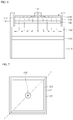
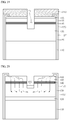
- FIGs. 1 and 2 are respectively a sectional view and a plan view of a light emitting device (LED) according to an embodiment 1.
- FIG. 1 is a vertical sectional view taken along a line I-I' of FIG. 2 .
- an LED according to an embodiment 1 may include: a first conductivity type semiconductor layer 130, an active layer 140, and a second conductivity type semiconductor layer 150 formed on a substrate 110; a first dielectric layer 171 covering the edges of the second conductivity type semiconductor layer 150 and the active layer 140; and a first electrode layer 135 covering the edge of the first conductivity type semiconductor layer 130.
- the first electrode layer 135 is formed also on the first dielectric layer 171, the embodiment is not limited thereto. That is, the first electrode layer 135 may not be formed on the first dielectric layer 171.
- the first electrode layer 135 is formed not only on the first conductivity type semiconductor layer 130 but also on the substrate 110 and a buffer layer 120, the embodiment is not limited thereto. That is, the first electrode layer 135 may be formed only on the first conductivity type semiconductor layer 130.
- the effective contact area is increased to improve current spreading and thermal characteristics.
- FIGs. 1 and 2 illustrate a method of forming an n-type electrode.
- the edges of the active layer 140, and the second conductivity type semiconductor layer 150 are partially etched and it is passivated by the first dielectric layer 171.
- an N-type electrode is formed by the first electrode layer 135 on the first conductivity type semiconductor layer 130, thereby uniformalizing current injection into an epitaxial layer.
- a non-etched LED chip is a 500 ⁇ m ⁇ 500 ⁇ m square chip in the plan view
- the region from each side to about 25 to 50 ⁇ m point of the square may be regarded as the edge to be removed, to which the present invention is not limited.
- the embodiment forms one of two electrodes on the edge of the exposed epitaxial layer in a lateral type structure, thereby making it possible to increase the current spreading effects through the outer electrode of the LED chip. Also, the embodiment can increase the current spreading effects through a chip isolation structure, thereby making it possible to dissipate heat through a wide area.
- the LED according to the embodiment 1 has a structure where the first electrode layer 135 is formed on the edge to implement an N-type electrode, as shown in FIGs. 1 and 2 .
- the embodiment 1 exposes the first conductivity type semiconductor layer 130 of the edge through an etching process; isolates it by the first dielectric layer 171 (e.g., a passivation layer); deposits the first electrode layer 135 thereon; and performs overall or partial soldering for a package with good thermal conductivity.
- the package may be a metal-based package, to which the embodiment is not limited.
- FIG. 1 Current flows are schematically shown in FIG. 1 . Currents flow from an upper p-type electrode 155 to the n-type electrode of the first electrode layer 135 formed on the edge, thus making it possible to achieve uniform current spreading effects.
- the embodiment 1 overcomes the problem of localized light emission, thus reducing unnecessary power consumption caused by the corresponding voltage and current.
- the embodiment 1 forms the n-type electrode on the edge to fabricate an LED chip, thus enabling bottom/side contacts with a package with good thermal conductivity through soldering.
- the first electrode layer 135 i.e., the n-type electrode on the edge
- FIG. is a sectional view of an LED package according to an embodiment 1, which shows the final sectional structure of the package for the LED chip structure of FIG. 1 .
- the first electrode layer 135 and a package metal body 210 contact with each other through a solder 220 to form the n-type electrode.
- a current according to chip driving can flow through the contact interface. Therefore, in comparison with the current injection by the two wire-bonding of the related art, the embodiment can reduce an operation voltage and can dissipate unnecessary heat caused by intra-chip heat emission.
- a current through the electrode on the chip edge can spread very well, thus enabling operation voltage reduction and attachment without wire bonding. Therefore, it is possible to provide one wire-bonding packaging.
- the thermal improvement is important for the package lifetime in a high-power application display, the reliability can be increased.
- the thermal conductivity of the bottom substrate used in the lateral type structure is relatively very low, the dissipation of generated heat to the outside is important.
- the embodiment can increase the current spreading effects through the chip isolation structure, thus making it possible to dissipate heat through a large area.
- the embodiment improves heat dissipation by contacting the package and the chip bottom portion through soldering, thereby making it possible to improve the current spreading and thermal characteristics by a small-area isolation structure of a large-area chip.
- the embodiment electrically isolates an upper p-type pad 250 from the package surface by a dielectric 230 and performs wire-bonding 255, so that a metal package forms one electrode and the upper p-type pad 250 forms another electrode.
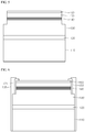
- FIGs. 4 to 7 are sectional views showing a process for fabricating an LED according to an embodiment 1.
- a substrate 110 is prepared.
- the substrate 110 may be a sapphire (Al 2 O 3 ) monocrystalline substrate, to which the embodiment is not limited.
- a wet cleaning process may be performed to remove the impurities of the surface of the substrate 110.
- a buffer layer 120 may be formed on the substrate 110.
- a first conductivity type semiconductor layer 130 is formed on the buffer layer 120.
- a chemical vapor deposition (CVD) process, a molecular beam epitaxy (MBE) process, a sputtering process, or a hydride vapor phase epitaxy (HVPE) process may be used to form the first conductivity type semiconductor layer 130.
- the first conductivity type semiconductor layer 130 may be formed by injecting tri-methyl gallium gas (TMGa), ammonia gas (NH 3 ), nitrogen gas (N 2 ), or silane gas (SiH 4 ) containing n-type impurity such as silicon (Si) into a process chamber.
- TMGa tri-methyl gallium gas
- NH 3 ammonia gas
- N 2 nitrogen gas
- SiH 4 silane gas
- An active layer 140 is formed on the first conductivity type semiconductor layer 130.
- the active layer 140 emits a light of energy determined by the specific energy band of the active layer material when electrons injected through the first conductivity type semiconductor layer 130 recombine with holes injected through a second conductivity type semiconductor layer 150.
- the active layer 140 may have a single or multi quantum well structure that is formed by alternately laminating nitride semiconductor layers with different energy bands once or several times.
- the active layer 140 may have a multiple quantum well structure with an InGaN/GaN structure that is formed by injecting tri-methyl gallium gas (TMGa), ammonia gas (NH 3 ), nitrogen gas (N 2 ), or tri-methyl indium gas (TMIn), to which the embodiment is not limited.
- TMGa tri-methyl gallium gas
- NH 3 ammonia gas
- N 2 nitrogen gas
- TIn tri-methyl indium gas
- a second conductivity type semiconductor layer 150 is formed on the active layer 140.
- the second conductivity type semiconductor layer 150 may be formed by injecting tri-methyl gallium gas (TMGa), ammonia gas (NH 3 ), nitrogen gas (N 2 ), hydrogen gas (H 2 ), or bisethylcyclopentadienyl magnesium (EtCp 2 Mg) ⁇ Mg(C 2 H 5 C 5 H 4 ) 2 ⁇ containing p-type impurity such as magnesium (Mg) into a process chamber, to which the embodiment is not limited.
- TMGa tri-methyl gallium gas
- NH 3 ammonia gas
- N 2 nitrogen gas
- H 2 hydrogen gas
- EtCp 2 Mg bisethylcyclopentadienyl magnesium
- An ohmic contact layer 160 is formed on the second conductivity type semiconductor layer 150.
- the ohmic contact layer 160 may be formed of at least one of ITO (Indium-Tin-Oxide), IZO (In-ZnO), GZO (Ga-ZnO), AZO (Al-ZnO), AGZO (Al-Ga ZnO), IGZO (In-Ga ZnO), IrOx, RuOx, RuOx/ITO, Ni/IrOx/Au, and Ni/IrOx/Au/ITO, to which the embodiment is not limited.
- the embodiment forms the ohmic contact layer, thereby making it possible to increase the electric conductivity and the light extraction efficiency.
- the current spreading through the ohmic contact layer 160 plays an important role for uniform distribution of light emission in the upper portion of the chip.
- the edges of the ohmic contact layer 160, the second conductivity type semiconductor layer 150, and the active layer 140 are removed to expose the first conductivity type semiconductor layer 130.
- a first pattern (not shown) is formed, and the first pattern is used as an etch mask to remove the edges of the ohmic contact layer 160, the second conductivity type semiconductor layer 150, and the active layer 140, thereby exposing the first conductivity type semiconductor layer 130.
- the first pattern may be formed of silicon nitride, silicon oxide, or photoresist. Thereafter, the first pattern may be removed through a wet etching process or an ashing process.
- the non-etched LED chip is a 500 ⁇ m ⁇ 500 ⁇ m square chip in the plan view
- the region from each side to about 25 to 50 ⁇ m point of the square may be regarded as the edge to be removed, to which the present invention is not limited.
- a first dielectric layer 171 is formed to cover the edges of the ohmic contact layer 160, the second conductivity type semiconductor layer 150 and the active layer 140.
- an oxide layer or a nitride layer may be used to form the first dielectric layer 171 (i.e., the passivation layer) on the surface of the epitaxial layer exposed to suppress a leakage current caused by surface instability.
- the first dielectric layer 171 serves to electrically isolate the active layer 140, the second conductivity type semiconductor layer 150, and a first electrode layer 135 to be formed later.
- a first electrode layer 135 is formed to cover the edges of the second conductivity type semiconductor layer 150, the active layer 140, the substrate 110, and the first conductivity type semiconductor layer 130.
- FIG. 6 illustrates that the first electrode layer 135 is formed also on the first dielectric layer 171, the embodiment is not limited thereto. That is, the first electrode layer 135 may not be formed on the first dielectric layer 171.
- the first electrode layer 135 is formed not only on the first conductivity type semiconductor layer 130 but also on the substrate 110 and the buffer layer 120, the embodiment is not limited thereto. That is, the first electrode layer 135 may be formed only on the first conductivity type semiconductor layer 130.
- the effective contact area is increased to improve current spreading and thermal characteristics.
- the first electrode layer 135 may be formed of a metal capable of reflecting light.
- the first electrode layer 135 may be formed of a metal layer containing aluminum (Al), argentum (Ag), or an Al or Ag-containing metal alloy that well reflects the light emitted from the active layer.
- one of the two electrodes is formed on the edge of the exposed epitaxial layer in the lateral type structure, thereby making it possible to increase the spreading effects through the LED chip edge electrode.
- a second electrode 155 is formed on the ohmic contact layer 160.
- one of the two electrodes is formed on the edge of the epitaxial layer in the lateral type structure, thereby making it possible to increase the current spreading effects through the LED chip edge electrode.
- the embodiment can increase the current spreading effects through the chip isolation structure, thus making it possible to dissipate heat through a wide area.
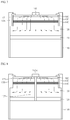
- FIGs. 8 and 9 are respectively a sectional view and a plan view of an LED according to an embodiment 2, which is an embodiment of the invention.
- FIG. 10 is a sectional view of an LED package according to an embodiment 2.
- FIG. 8 is a sectional view taken along a line II-II' of FIG. 9 .
- the embodiment 2 may use the technical features of the embodiment 1. Hereinafter, a description of an overlap with the embodiment 1 will be omitted for conciseness.
- the embodiment 2 includes a second dielectric layer 172 that divides the second conductivity type semiconductor layer 150, the active layer 140, and the first conductivity type semiconductor layer 130 into a plurality of regions.
- the embodiment 2 divides the epitaxial layer into quartered squares through an etching process and distributes a current flow of a large-area chip to the quartered regions, thereby making it possible to improve the uniformity and suppress the localized heat generation.
- the epitaxial layer may also be divided into two or three equal parts.
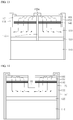
- FIGs. 11 to 13 are sectional views showing a process for fabricating an LED according to an embodiment 2.
- a first conductivity type semiconductor layer 130, an active layer 140, and a second conductivity type semiconductor layer 150 are formed on a substrate 110.
- a buffer layer 120 is further formed on the substrate 110 and an ohmic contact layer 160 may be further formed on the second conductivity type semiconductor layer 150.
- the edges of the ohmic contact layer 160, the second conductivity type semiconductor layer 150, and the active layer 140 are removed to expose the first conductivity type semiconductor layer 130.
- the embodiment 2 forms a second trench T2 that divides the ohmic contact layer 160, the second conductivity type semiconductor layer 150, the active layer 140, and the first conductivity type semiconductor layer 130 into a plurality of regions.
- a first dielectric layer 171 is formed to cover the edges of the ohmic contact layer 160, the second conductivity type semiconductor layer 150 and the active layer 140, and the exposed first conductivity type semiconductor layer 130.
- a second dielectric layer 172 is formed to fill the second trench T2.
- the dielectric layer on the ohmic contact layer 160 is removed, thereby forming the first dielectric layer 171 and the second dielectric layer 172 simultaneously.
- the embodiment 2 divides the epitaxial layer into quartered squares through an etching process and distributes a current flow of a large-area chip to the quartered regions, thereby making it possible to improve the uniformity and suppress the localized heat generation.
- the epitaxial layer may also be divided into two or three equal parts.
- a first electrode layer 135 may be formed to cover the edges of the ohmic contact layer 160 with the first dielectric layer 171, the second conductivity type semiconductor layer 150, the active layer 140, the substrate 110, and the first conductivity type semiconductor layer 130.
- a common second electrode 155a is formed on the divided second conductivity type semiconductor layer 150 or the ohmic contact layer 160.
- the common second electrode 155a is formed to contact all of the divided second conductivity type semiconductor layers 150 or the divided ohmic contact layers 160.
- the first electrode layer 135 and the common second electrode 155a may be simultaneously formed of the same material.
- a metal layer is formed to cover the LED chip, and the metal layer is removed to leave the metal layer on the common second electrode 155a and expose the first dielectric layer 171, thereby forming the first electrode layer 135 and the common second electrode 155a simultaneously.
- FIGs. 14 and 15 are respectively a sectional view and a plan view of an LED according to an embodiment 3.
- FIG. 16 is a sectional view of an LED package according to an embodiment 3.
- FIG. 14 is a vertical sectional view taken along a line III-III' of FIG. 15 .
- the embodiment 3 may use the technical features of the embodiment 1. Hereinafter, a description of an overlap with the embodiment 1 will be omitted for conciseness.
- the LED according to the embodiment 3 may include: a first conductivity type semiconductor layer 130, an active layer 140, a second conductivity type semiconductor layer 150 formed sequentially on a substrate 110; a first electrode 133 formed on the center of the first conductivity type semiconductor layer 130 exposed by removing the portions of the active region 140 and the second conductivity type semiconductor layer 150; a third dielectric layer 173 covering the edges of the substrate 110, the first conductivity type semiconductor layer 130, the active layer 140 and the second conductivity type semiconductor layer 150; and a second electrode layer 157 around the upper portion of the second conductivity type semiconductor layer 150.
- the embodiment 3 implements the second electrode layer 157 to be uses as a p-type electrode at the edge.
- the embodiment 3 etches the centers of the ohmic contact layer 160, the second conductivity type semiconductor layer 150 and the active layer 140, and forms an n-type electrode 133 in the center region of the first conductivity type semiconductor layer 130.
- the n-type electrode 133 is wire-bonded to an N-type pad 235.
- FIGs. 17 to 20 are sectional views showing a process for fabricating an LED according to an embodiment 3.
- a buffer layer 120, a first conductivity type semiconductor layer 130, an active layer 140, a second conductivity type semiconductor layer 150, and an ohmic contact layer 160 are formed on a substrate 110.
- a third dielectric layer 173 is formed to cover the edges of the substrate 110, the buffer layer 120, the first conductivity type semiconductor layer 130, the active layer 140, the ohmic contact layer 160, and the second conductivity type semiconductor layer 150.
- an oxide layer or a nitride layer is used to form a passivation layer (i.e., the third dielectric layer 173), thereby providing an electrical isolation from a second electrode layer 157 to be formed later.
- a second electrode layer 157 is formed around the upper portion of the second conductivity type semiconductor layer 150.
- the second electrode layer 157 may be formed to cover the third dielectric layer 173.
- the second electrode layer 157 may be formed of a metal capable of reflecting light, to which the embodiment is not limited.
- a first pattern 310 as a mask, the portions of the centers of the ohmic contact layer 160, the second conductivity type semiconductor layer 150 and the active layer 140 are removed to expose the first conductivity type semiconductor layer 130.
- a first trench T1 may be formed to remove the portions of the centers of the ohmic contact layer 160, the second conductivity type semiconductor layer 150 and the active layer 140 are removed to expose the first conductivity type semiconductor layer 130.
- the first pattern 310 may be a photoresist, an oxide layer, or a nitride layer.
- a first electrode 133 may be formed on the exposed first conductivity type semiconductor layer 130.
- the first electrode 133 may be formed on the first conductivity type semiconductor layer 130, by filling the first trench T1 with the first pattern 310 unremoved and removing the first pattern 310 through an ashing process or an etching process.
- FIGs. 21 and 22 are respectively a sectional view and a plan view of an LED according to an embodiment 4, which is an embodiment of the invention.
- FIG. 23 is a sectional view of an LED package according to an embodiment 4.
- FIG. 21 is a vertical sectional view taken along a line IV-IV' of FIG. 22 .
- the embodiment 4 may use the technical features of the embodiments 1 to 3. Hereinafter, a description of an overlap with the embodiments 1 to 3 will be omitted for conciseness.
- the embodiment 4 includes a fourth dielectric layer 174 that divides the ohmic contact layer 160, the second conductivity type semiconductor layer 150, the active layer 140, and the first conductivity type semiconductor layer 130 into a plurality of regions.
- the embodiment 4 divides the epitaxial layer into quartered squares through an etching process and distributes a current flow of a large-area chip to the quartered regions, thereby making it possible to improve the uniformity and suppress the localized heat generation.
- the epitaxial layer may also be divided into two or three equal parts.
- FIGs. 24 to 27 are sectional views showing a process for fabricating an LED according to an embodiment 4.
- a buffer layer 120, a first conductivity type semiconductor layer 130, an active layer 140, a second conductivity type semiconductor layer 150, and an ohmic contact layer 160 are sequentially formed on a substrate 110.
- a second pattern 320 used as a mask to form a second trench T2 that divide the ohmic contact layer 150, the second conductivity type semiconductor layer 150, the active layer 140, the first conductivity type semiconductor layer 130 and the buffer layer 120 into a plurality of regions.
- the second pattern 320 may be a photoresist or a dielectric.
- the second pattern 320 is removed, and a third pattern 330 is used as a mask to remove the portions of the centers of the ohmic contact layer 160, the second conductivity type semiconductor layer 150 and the active layer 140 to expose the first conductivity type semiconductor layer 130.
- a first trench T1 may be formed to remove the portions of the centers of the ohmic contact layer 160, the second conductivity type semiconductor layer 150 and the active layer 140.
- the third pattern 330 may be removed through an ashing process or an etching process, a fourth dielectric layer 174 may be formed to fill the second trench T2, and a third dielectric layer 173 may be formed to cover the edges of the ohmic contact layer 160, the second conductivity type semiconductor layer 150, the active layer 140, the first conductivity type semiconductor layer 130, the buffer layer 120, and the substrate 110.
- a dielectric layer (not shown) is formed on the chip without the third pattern 330, and the dielectric layer on the ohmic contact layer 160 and the first trench T1 is removed to simultaneously form the fourth dielectric layer 174 and the third dielectric layer 173, to which the embodiment is not limited.
- a second electrode layer 157 may be formed to cover the edges of the ohmic contact layer 160 with the third dielectric layer 173, the second conductivity type semiconductor layer 150, the active layer 140, the substrate 110 and the first conductivity type semiconductor layer 130.
- a common first electrode 133a is formed on the exposed first conductivity type semiconductor layer 130 and the fourth dielectric layer 174.
- the common first electrode 133a is formed to contact all of the divided first conductivity type semiconductor layers 130.
- the second electrode layer 157 and the common first electrode 133a may be formed simultaneously.
- a metal layer (not shown) is formed to cover the LED chip; a portion of the metal on the first trench T1 is removed to form the common first electrode 133a by leaving the metal layer to contact only the first conductivity type semiconductor layer 130; and a portion of the metal layer on the ohmic contact layer 160, thereby forming the second electrode layer 157 and the common first electrode 133a simultaneously.
- the embodiment 4 divides the epitaxial layer into quartered squares through an etching process and distributes a current flow of a large-area chip to the quartered regions, thereby making it possible to improve the uniformity and suppress the localized heat generation.
- the epitaxial layer may also be divided into two or three equal parts.
- a current according to chip driving can flow through the contact interface. Therefore, in comparison with the current injection by the two wire-bonding of the related art, the embodiment can reduce an operation voltage and can dissipate unnecessary heat caused by intra-chip heat emission.
- a current through the electrode on the chip edge can spread very well, thus enabling operation voltage reduction and attachment without wire bonding. Therefore, it is possible to provide one wire-bonding packaging.
- the embodiment can increase the current spreading effects through the chip isolation structure, thus making it possible to dissipate heat through a large area.
- the embodiment improves heat dissipation by contacting the package and the chip bottom portion through soldering, thereby making it possible to improve the current spreading and thermal characteristics by a small-area isolation structure of a large-area chip.
- a structure of a light emitting device includes a package
- the light emitting device can obtain high extraction efficiency regardless of a package structure.
Landscapes
- Led Devices (AREA)
Claims (9)
- Dispositif électroluminescent (LED) comportant :une couche de semi-conducteur d'un premier type de conductivité (130), une couche active (140) et une couche de semi-conducteur d'un second type de conductivité (150) sur un substrat (110),une première couche diélectrique (171) recouvrant les bords de la couche de semi-conducteur du second type de conductivité (150) et de la couche active (140),une seconde couche diélectrique (172) qui divise la couche de semi-conducteur du second type de conductivité, la couche active et la couche de semi-conducteur du premier type de conductivité en une pluralité de régions, et une première couche d'électrode (135) recouvrant le bord de la couche de semi-conducteur du premier type de conductivité (130), dans lequel la première couche d'électrode (135) s'étend jusqu'au substrat (110), etune seconde électrode (155a) qui chevauche verticalement la seconde couche diélectrique,dans lequel la seconde électrode (155a) est en contact avec la totalité de la couche de semi-conducteur du second type de conductivité divisée (150),caractérisé parla première couche d'électrode (135) étant en contact avec le bord du substrat (110), etune couche tampon (120) entre le substrat (110) et le semi-conducteur du premier type de conductivité (130),dans lequel la seconde couche diélectrique (172) divise la couche tampon (120) en une pluralité de régions.
- LED selon la revendication 1, dans lequel la première couche diélectrique (171) et la seconde couche diélectrique (172) sont formées du même matériau.
- LED selon la revendication 1, dans lequel la seconde électrode commune (155a) la première couche d'électrode (135) sont formées du même matériau.
- LED selon la revendication 1, dans lequel la première couche d'électrode (135) comporte une couche de métal réflectrice.
- LED selon la revendication 1, comportant une couche de contact ohmique sur la couche de semi-conducteur du second type de conductivité (150).
- Dispositif électroluminescent (LED) comportant :une structure électroluminescente comportant une couche de semi-conducteur d'un premier type de conductivité (130), une couche active (140) et couche de semi-conducteur d'un second type de conductivité (150) sur un substrat (110),une première électrode (133a) sur la couche de semi-conducteur du premier type de conductivité (130), dans lequel ces parties de la couche active (140) et la couche de semi-conducteur du second type de conductivité (150) qui chevauchent verticalement ladite couche d'électrode (133) sont manquantes,une première couche diélectrique (173) recouvrant le bord de la couche active (140) et la couche de semi-conducteur du premier type de conductivité (130),une seconde couche diélectrique (174) qui divise la couche de semi-conducteur du second type de conductivité, la couche active et la couche de semi-conducteur du premier type de conductivité en une pluralité de régions, etune seconde couche d'électrode (157) sur la couche de semi-conducteur du second type de conductivité (150),dans lequel la première électrode (133a) chevauche verticalement la seconde couche diélectrique (174), etdans lequel la première électrode (133a) est en contact avec la totalité de la couche de semi-conducteur du premier type de conductivité divisée,caractérisé parune couche tampon (120) entre le substrat (110) et la couche de semi-conducteur du premier type de conductivité (130),dans lequel la seconde couche diélectrique (174) divise la couche tampon (120) en une pluralité de régions.
- LED selon la revendication 6, dans lequel la seconde couche d'électrode (157) recouvre une partie de la première couche diélectrique (173).
- LED selon la revendication 7, dans lequel la première couche diélectrique (173) et la seconde couche diélectrique (174) sont formées du même matériau.
- Boîtier de dispositif électroluminescent (LED) comportant :un LED selon l'une quelconque des revendications précédentes.
Applications Claiming Priority (2)
| Application Number | Priority Date | Filing Date | Title |
|---|---|---|---|
| KR1020090013754A KR101007128B1 (ko) | 2009-02-19 | 2009-02-19 | 발광소자 및 그 제조방법 |
| PCT/KR2009/003039 WO2010095785A1 (fr) | 2009-02-19 | 2009-06-05 | Del et boîtier de del |
Publications (3)
| Publication Number | Publication Date |
|---|---|
| EP2400565A1 EP2400565A1 (fr) | 2011-12-28 |
| EP2400565A4 EP2400565A4 (fr) | 2015-06-03 |
| EP2400565B1 true EP2400565B1 (fr) | 2017-09-20 |
Family
ID=42634048
Family Applications (1)
| Application Number | Title | Priority Date | Filing Date |
|---|---|---|---|
| EP09840461.9A Not-in-force EP2400565B1 (fr) | 2009-02-19 | 2009-06-05 | Del et boîtier de del |
Country Status (5)
| Country | Link |
|---|---|
| US (1) | US8680560B2 (fr) |
| EP (1) | EP2400565B1 (fr) |
| KR (1) | KR101007128B1 (fr) |
| CN (1) | CN102187483B (fr) |
| WO (1) | WO2010095785A1 (fr) |
Families Citing this family (14)
| Publication number | Priority date | Publication date | Assignee | Title |
|---|---|---|---|---|
| TWI403003B (zh) * | 2009-10-02 | 2013-07-21 | Chi Mei Lighting Tech Corp | 發光二極體及其製造方法 |
| US9847372B2 (en) * | 2011-12-01 | 2017-12-19 | Micron Technology, Inc. | Solid state transducer devices with separately controlled regions, and associated systems and methods |
| US10115862B2 (en) * | 2011-12-27 | 2018-10-30 | eLux Inc. | Fluidic assembly top-contact LED disk |
| CN102646769B (zh) * | 2012-03-30 | 2015-08-05 | 达亮电子(苏州)有限公司 | 发光二极管组件、发光二极管封装结构及其制造方法 |
| FR3008547B1 (fr) * | 2013-07-15 | 2016-12-09 | Commissariat Energie Atomique | Structure emissive a injection laterale de porteurs |
| CN103606617B (zh) * | 2013-11-08 | 2016-06-29 | 溧阳市江大技术转移中心有限公司 | 具有透明电极的倒装发光二极管 |
| KR102119851B1 (ko) * | 2014-01-28 | 2020-06-05 | 엘지이노텍 주식회사 | 발광소자 |
| JP6606946B2 (ja) * | 2015-09-21 | 2019-11-20 | 豊田合成株式会社 | 発光素子 |
| US20180309025A1 (en) * | 2015-10-29 | 2018-10-25 | Kyocera Corporation | Light-emitting device, light receiving and emitting device module, and optical sensor |
| WO2018107323A1 (fr) * | 2016-12-12 | 2018-06-21 | Goertek. Inc | Procédé de fabrication de dispositif d'affichage, dispositif d'affichage et appareil d'électronique |
| US11749790B2 (en) * | 2017-12-20 | 2023-09-05 | Lumileds Llc | Segmented LED with embedded transistors |
| KR102608987B1 (ko) * | 2018-09-07 | 2023-12-05 | 삼성디스플레이 주식회사 | 발광 소자, 그의 제조 방법, 및 발광 소자를 구비한 표시 장치 |
| FR3105880B1 (fr) * | 2019-12-26 | 2023-09-15 | Commissariat Energie Atomique | Diode comportant au moins deux couches de passivation, en particulier formées de diélectrique, localement superposées pour optimiser la passivation |
| CN113555480B (zh) * | 2021-08-18 | 2022-10-18 | 江西乾照光电有限公司 | 一种具有侧壁异形电极结构的led芯片 |
Family Cites Families (16)
| Publication number | Priority date | Publication date | Assignee | Title |
|---|---|---|---|---|
| JP3136672B2 (ja) * | 1991-07-16 | 2001-02-19 | 豊田合成株式会社 | 窒化ガリウム系化合物半導体発光素子 |
| JPH0730153A (ja) | 1993-07-14 | 1995-01-31 | Hitachi Cable Ltd | 発光ダイオードチップ、その台座、及び発光ダイオード |
| JP3303154B2 (ja) * | 1994-09-30 | 2002-07-15 | ローム株式会社 | 半導体発光素子 |
| JP3557033B2 (ja) * | 1995-03-24 | 2004-08-25 | 三洋電機株式会社 | 半導体発光素子およびその製造方法 |
| JP3333356B2 (ja) | 1995-07-12 | 2002-10-15 | 株式会社東芝 | 半導体装置 |
| JPH09129922A (ja) | 1995-10-31 | 1997-05-16 | Sanyo Electric Co Ltd | 発光素子と発光素子の製造方法 |
| US6255129B1 (en) * | 2000-09-07 | 2001-07-03 | Highlink Technology Corporation | Light-emitting diode device and method of manufacturing the same |
| KR100463957B1 (ko) | 2000-10-02 | 2004-12-30 | 하이링크 테크놀로지 코포레이션 | 발광 다이오드 장치를 제조하는 방법 |
| JP2002368275A (ja) * | 2001-06-11 | 2002-12-20 | Toyoda Gosei Co Ltd | 半導体素子及びその製造方法 |
| JP2003110139A (ja) | 2001-09-28 | 2003-04-11 | Sanyo Electric Co Ltd | 窒化物系半導体発光素子 |
| KR100495004B1 (ko) * | 2002-07-09 | 2005-06-10 | 엘지이노텍 주식회사 | 발광다이오드 및 그 제조방법 |
| US6693306B2 (en) * | 2002-07-22 | 2004-02-17 | United Epitaxy Company, Ltd. | Structure of a light emitting diode and method of making the same |
| EP1652238B1 (fr) * | 2003-08-08 | 2010-10-27 | Kang, Sang-kyu | Micro-diode electroluminescente au nitrure a haute brillance et son procede de fabrication |
| TWI331406B (en) * | 2005-12-14 | 2010-10-01 | Advanced Optoelectronic Tech | Single chip with multi-led |
| KR100845856B1 (ko) | 2006-12-21 | 2008-07-14 | 엘지전자 주식회사 | 발광 소자 패키지 및 그 제조방법 |
| CN101222015B (zh) * | 2008-01-19 | 2010-05-12 | 鹤山丽得电子实业有限公司 | 发光二极管、具有其的封装结构及其制造方法 |
-
2009
- 2009-02-19 KR KR1020090013754A patent/KR101007128B1/ko not_active Expired - Fee Related
- 2009-06-05 US US12/990,170 patent/US8680560B2/en not_active Expired - Fee Related
- 2009-06-05 CN CN200980141602.6A patent/CN102187483B/zh not_active Expired - Fee Related
- 2009-06-05 WO PCT/KR2009/003039 patent/WO2010095785A1/fr not_active Ceased
- 2009-06-05 EP EP09840461.9A patent/EP2400565B1/fr not_active Not-in-force
Non-Patent Citations (1)
| Title |
|---|
| None * |
Also Published As
| Publication number | Publication date |
|---|---|
| KR101007128B1 (ko) | 2011-01-10 |
| US8680560B2 (en) | 2014-03-25 |
| KR20100094671A (ko) | 2010-08-27 |
| WO2010095785A1 (fr) | 2010-08-26 |
| CN102187483A (zh) | 2011-09-14 |
| EP2400565A1 (fr) | 2011-12-28 |
| CN102187483B (zh) | 2015-04-01 |
| US20110133221A1 (en) | 2011-06-09 |
| EP2400565A4 (fr) | 2015-06-03 |
Similar Documents
| Publication | Publication Date | Title |
|---|---|---|
| EP2400565B1 (fr) | Del et boîtier de del | |
| EP2221873B1 (fr) | Dispositif électroluminescent | |
| EP2432036B1 (fr) | Diode électroluminescente | |
| KR101064053B1 (ko) | 발광소자 및 그 제조방법 | |
| JP5816243B2 (ja) | 発光素子及び発光素子パッケージ | |
| EP2439796B1 (fr) | Dispositif électroluminescent et système d'éclairage | |
| KR100986556B1 (ko) | 발광소자 및 그 제조방법 | |
| US8829538B2 (en) | Light emitting device package | |
| EP2251916A1 (fr) | Dispositif électroluminescent, conditionnement de dispositif électroluminescent et système d'éclairage l'incluant | |
| EP2482318B1 (fr) | Dispositif électroluminescent | |
| KR101007145B1 (ko) | 발광소자 칩, 발광소자 패키지 및 발광소자 칩의 제조방법 | |
| EP2221886B1 (fr) | Dispositif électroluminescent à semiconducteur | |
| US9130123B2 (en) | Light emitting device and light emitting device package | |
| KR20160145413A (ko) | 적색 발광소자, 적색 발광소자의 제조방법 및 발광소자 패키지 | |
| KR101746842B1 (ko) | 발광소자, 발광소자의 제조방법 및 발광소자 패키지 | |
| KR20110069376A (ko) | 반도체 발광소자 제조방법 및 이에 의하여 제조된 반도체 발광소자 |
Legal Events
| Date | Code | Title | Description |
|---|---|---|---|
| PUAI | Public reference made under article 153(3) epc to a published international application that has entered the european phase |
Free format text: ORIGINAL CODE: 0009012 |
|
| 17P | Request for examination filed |
Effective date: 20110912 |
|
| AK | Designated contracting states |
Kind code of ref document: A1 Designated state(s): AT BE BG CH CY CZ DE DK EE ES FI FR GB GR HR HU IE IS IT LI LT LU LV MC MK MT NL NO PL PT RO SE SI SK TR |
|
| DAX | Request for extension of the european patent (deleted) | ||
| RA4 | Supplementary search report drawn up and despatched (corrected) |
Effective date: 20150508 |
|
| RIC1 | Information provided on ipc code assigned before grant |
Ipc: H01L 33/44 20100101AFI20150430BHEP Ipc: H01L 33/08 20100101ALN20150430BHEP Ipc: H01L 33/20 20100101ALN20150430BHEP |
|
| 17Q | First examination report despatched |
Effective date: 20160307 |
|
| REG | Reference to a national code |
Ref country code: DE Ref legal event code: R079 Ref document number: 602009048495 Country of ref document: DE Free format text: PREVIOUS MAIN CLASS: H01L0033360000 Ipc: H01L0033440000 |
|
| GRAP | Despatch of communication of intention to grant a patent |
Free format text: ORIGINAL CODE: EPIDOSNIGR1 |
|
| RIC1 | Information provided on ipc code assigned before grant |
Ipc: H01L 33/44 20100101AFI20170309BHEP Ipc: H01L 33/20 20100101ALN20170309BHEP Ipc: H01L 33/08 20100101ALN20170309BHEP |
|
| INTG | Intention to grant announced |
Effective date: 20170411 |
|
| RAP1 | Party data changed (applicant data changed or rights of an application transferred) |
Owner name: LG INNOTEK CO., LTD. |
|
| GRAS | Grant fee paid |
Free format text: ORIGINAL CODE: EPIDOSNIGR3 |
|
| GRAA | (expected) grant |
Free format text: ORIGINAL CODE: 0009210 |
|
| AK | Designated contracting states |
Kind code of ref document: B1 Designated state(s): AT BE BG CH CY CZ DE DK EE ES FI FR GB GR HR HU IE IS IT LI LT LU LV MC MK MT NL NO PL PT RO SE SI SK TR |
|
| REG | Reference to a national code |
Ref country code: GB Ref legal event code: FG4D |
|
| REG | Reference to a national code |
Ref country code: CH Ref legal event code: EP |
|
| REG | Reference to a national code |
Ref country code: AT Ref legal event code: REF Ref document number: 930792 Country of ref document: AT Kind code of ref document: T Effective date: 20171015 |
|
| REG | Reference to a national code |
Ref country code: IE Ref legal event code: FG4D |
|
| REG | Reference to a national code |
Ref country code: DE Ref legal event code: R096 Ref document number: 602009048495 Country of ref document: DE |
|
| REG | Reference to a national code |
Ref country code: NL Ref legal event code: MP Effective date: 20170920 |
|
| PG25 | Lapsed in a contracting state [announced via postgrant information from national office to epo] |
Ref country code: SE Free format text: LAPSE BECAUSE OF FAILURE TO SUBMIT A TRANSLATION OF THE DESCRIPTION OR TO PAY THE FEE WITHIN THE PRESCRIBED TIME-LIMIT Effective date: 20170920 Ref country code: LT Free format text: LAPSE BECAUSE OF FAILURE TO SUBMIT A TRANSLATION OF THE DESCRIPTION OR TO PAY THE FEE WITHIN THE PRESCRIBED TIME-LIMIT Effective date: 20170920 Ref country code: NO Free format text: LAPSE BECAUSE OF FAILURE TO SUBMIT A TRANSLATION OF THE DESCRIPTION OR TO PAY THE FEE WITHIN THE PRESCRIBED TIME-LIMIT Effective date: 20171220 Ref country code: FI Free format text: LAPSE BECAUSE OF FAILURE TO SUBMIT A TRANSLATION OF THE DESCRIPTION OR TO PAY THE FEE WITHIN THE PRESCRIBED TIME-LIMIT Effective date: 20170920 Ref country code: HR Free format text: LAPSE BECAUSE OF FAILURE TO SUBMIT A TRANSLATION OF THE DESCRIPTION OR TO PAY THE FEE WITHIN THE PRESCRIBED TIME-LIMIT Effective date: 20170920 |
|
| REG | Reference to a national code |
Ref country code: LT Ref legal event code: MG4D |
|
| REG | Reference to a national code |
Ref country code: AT Ref legal event code: MK05 Ref document number: 930792 Country of ref document: AT Kind code of ref document: T Effective date: 20170920 |
|
| PG25 | Lapsed in a contracting state [announced via postgrant information from national office to epo] |
Ref country code: LV Free format text: LAPSE BECAUSE OF FAILURE TO SUBMIT A TRANSLATION OF THE DESCRIPTION OR TO PAY THE FEE WITHIN THE PRESCRIBED TIME-LIMIT Effective date: 20170920 Ref country code: BG Free format text: LAPSE BECAUSE OF FAILURE TO SUBMIT A TRANSLATION OF THE DESCRIPTION OR TO PAY THE FEE WITHIN THE PRESCRIBED TIME-LIMIT Effective date: 20171220 Ref country code: GR Free format text: LAPSE BECAUSE OF FAILURE TO SUBMIT A TRANSLATION OF THE DESCRIPTION OR TO PAY THE FEE WITHIN THE PRESCRIBED TIME-LIMIT Effective date: 20171221 |
|
| PG25 | Lapsed in a contracting state [announced via postgrant information from national office to epo] |
Ref country code: NL Free format text: LAPSE BECAUSE OF FAILURE TO SUBMIT A TRANSLATION OF THE DESCRIPTION OR TO PAY THE FEE WITHIN THE PRESCRIBED TIME-LIMIT Effective date: 20170920 |
|
| PG25 | Lapsed in a contracting state [announced via postgrant information from national office to epo] |
Ref country code: CZ Free format text: LAPSE BECAUSE OF FAILURE TO SUBMIT A TRANSLATION OF THE DESCRIPTION OR TO PAY THE FEE WITHIN THE PRESCRIBED TIME-LIMIT Effective date: 20170920 Ref country code: PL Free format text: LAPSE BECAUSE OF FAILURE TO SUBMIT A TRANSLATION OF THE DESCRIPTION OR TO PAY THE FEE WITHIN THE PRESCRIBED TIME-LIMIT Effective date: 20170920 Ref country code: ES Free format text: LAPSE BECAUSE OF FAILURE TO SUBMIT A TRANSLATION OF THE DESCRIPTION OR TO PAY THE FEE WITHIN THE PRESCRIBED TIME-LIMIT Effective date: 20170920 Ref country code: RO Free format text: LAPSE BECAUSE OF FAILURE TO SUBMIT A TRANSLATION OF THE DESCRIPTION OR TO PAY THE FEE WITHIN THE PRESCRIBED TIME-LIMIT Effective date: 20170920 |
|
| PG25 | Lapsed in a contracting state [announced via postgrant information from national office to epo] |
Ref country code: IT Free format text: LAPSE BECAUSE OF FAILURE TO SUBMIT A TRANSLATION OF THE DESCRIPTION OR TO PAY THE FEE WITHIN THE PRESCRIBED TIME-LIMIT Effective date: 20170920 Ref country code: AT Free format text: LAPSE BECAUSE OF FAILURE TO SUBMIT A TRANSLATION OF THE DESCRIPTION OR TO PAY THE FEE WITHIN THE PRESCRIBED TIME-LIMIT Effective date: 20170920 Ref country code: SK Free format text: LAPSE BECAUSE OF FAILURE TO SUBMIT A TRANSLATION OF THE DESCRIPTION OR TO PAY THE FEE WITHIN THE PRESCRIBED TIME-LIMIT Effective date: 20170920 Ref country code: IS Free format text: LAPSE BECAUSE OF FAILURE TO SUBMIT A TRANSLATION OF THE DESCRIPTION OR TO PAY THE FEE WITHIN THE PRESCRIBED TIME-LIMIT Effective date: 20180120 Ref country code: EE Free format text: LAPSE BECAUSE OF FAILURE TO SUBMIT A TRANSLATION OF THE DESCRIPTION OR TO PAY THE FEE WITHIN THE PRESCRIBED TIME-LIMIT Effective date: 20170920 |
|
| REG | Reference to a national code |
Ref country code: DE Ref legal event code: R097 Ref document number: 602009048495 Country of ref document: DE |
|
| PLBE | No opposition filed within time limit |
Free format text: ORIGINAL CODE: 0009261 |
|
| STAA | Information on the status of an ep patent application or granted ep patent |
Free format text: STATUS: NO OPPOSITION FILED WITHIN TIME LIMIT |
|
| PG25 | Lapsed in a contracting state [announced via postgrant information from national office to epo] |
Ref country code: DK Free format text: LAPSE BECAUSE OF FAILURE TO SUBMIT A TRANSLATION OF THE DESCRIPTION OR TO PAY THE FEE WITHIN THE PRESCRIBED TIME-LIMIT Effective date: 20170920 |
|
| 26N | No opposition filed |
Effective date: 20180621 |
|
| PG25 | Lapsed in a contracting state [announced via postgrant information from national office to epo] |
Ref country code: SI Free format text: LAPSE BECAUSE OF FAILURE TO SUBMIT A TRANSLATION OF THE DESCRIPTION OR TO PAY THE FEE WITHIN THE PRESCRIBED TIME-LIMIT Effective date: 20170920 |
|
| REG | Reference to a national code |
Ref country code: CH Ref legal event code: PL |
|
| GBPC | Gb: european patent ceased through non-payment of renewal fee |
Effective date: 20180605 |
|
| REG | Reference to a national code |
Ref country code: BE Ref legal event code: MM Effective date: 20180630 |
|
| REG | Reference to a national code |
Ref country code: IE Ref legal event code: MM4A |
|
| PG25 | Lapsed in a contracting state [announced via postgrant information from national office to epo] |
Ref country code: LU Free format text: LAPSE BECAUSE OF NON-PAYMENT OF DUE FEES Effective date: 20180605 Ref country code: MC Free format text: LAPSE BECAUSE OF FAILURE TO SUBMIT A TRANSLATION OF THE DESCRIPTION OR TO PAY THE FEE WITHIN THE PRESCRIBED TIME-LIMIT Effective date: 20170920 |
|
| PG25 | Lapsed in a contracting state [announced via postgrant information from national office to epo] |
Ref country code: FR Free format text: LAPSE BECAUSE OF NON-PAYMENT OF DUE FEES Effective date: 20180630 Ref country code: IE Free format text: LAPSE BECAUSE OF NON-PAYMENT OF DUE FEES Effective date: 20180605 Ref country code: GB Free format text: LAPSE BECAUSE OF NON-PAYMENT OF DUE FEES Effective date: 20180605 Ref country code: LI Free format text: LAPSE BECAUSE OF NON-PAYMENT OF DUE FEES Effective date: 20180630 Ref country code: CH Free format text: LAPSE BECAUSE OF NON-PAYMENT OF DUE FEES Effective date: 20180630 |
|
| PG25 | Lapsed in a contracting state [announced via postgrant information from national office to epo] |
Ref country code: BE Free format text: LAPSE BECAUSE OF NON-PAYMENT OF DUE FEES Effective date: 20180630 |
|
| PG25 | Lapsed in a contracting state [announced via postgrant information from national office to epo] |
Ref country code: MT Free format text: LAPSE BECAUSE OF NON-PAYMENT OF DUE FEES Effective date: 20180605 |
|
| PG25 | Lapsed in a contracting state [announced via postgrant information from national office to epo] |
Ref country code: TR Free format text: LAPSE BECAUSE OF FAILURE TO SUBMIT A TRANSLATION OF THE DESCRIPTION OR TO PAY THE FEE WITHIN THE PRESCRIBED TIME-LIMIT Effective date: 20170920 |
|
| PG25 | Lapsed in a contracting state [announced via postgrant information from national office to epo] |
Ref country code: HU Free format text: LAPSE BECAUSE OF FAILURE TO SUBMIT A TRANSLATION OF THE DESCRIPTION OR TO PAY THE FEE WITHIN THE PRESCRIBED TIME-LIMIT; INVALID AB INITIO Effective date: 20090605 Ref country code: PT Free format text: LAPSE BECAUSE OF FAILURE TO SUBMIT A TRANSLATION OF THE DESCRIPTION OR TO PAY THE FEE WITHIN THE PRESCRIBED TIME-LIMIT Effective date: 20170920 |
|
| PG25 | Lapsed in a contracting state [announced via postgrant information from national office to epo] |
Ref country code: CY Free format text: LAPSE BECAUSE OF FAILURE TO SUBMIT A TRANSLATION OF THE DESCRIPTION OR TO PAY THE FEE WITHIN THE PRESCRIBED TIME-LIMIT Effective date: 20170920 Ref country code: MK Free format text: LAPSE BECAUSE OF NON-PAYMENT OF DUE FEES Effective date: 20170920 |
|
| REG | Reference to a national code |
Ref country code: DE Ref legal event code: R081 Ref document number: 602009048495 Country of ref document: DE Owner name: SUZHOU LEKIN SEMICONDUCTOR CO. LTD., TAICANG, CN Free format text: FORMER OWNER: LG INNOTEK CO., LTD., SEOUL, KR |
|
| PGFP | Annual fee paid to national office [announced via postgrant information from national office to epo] |
Ref country code: DE Payment date: 20230502 Year of fee payment: 15 |
|
| REG | Reference to a national code |
Ref country code: DE Ref legal event code: R079 Ref document number: 602009048495 Country of ref document: DE Free format text: PREVIOUS MAIN CLASS: H01L0033440000 Ipc: H10H0020840000 |
|
| REG | Reference to a national code |
Ref country code: DE Ref legal event code: R119 Ref document number: 602009048495 Country of ref document: DE |
|
| PG25 | Lapsed in a contracting state [announced via postgrant information from national office to epo] |
Ref country code: DE Free format text: LAPSE BECAUSE OF NON-PAYMENT OF DUE FEES Effective date: 20250101 |