EP2403005A1 - Verfahren zur herstellung von solarzellen - Google Patents
Verfahren zur herstellung von solarzellen Download PDFInfo
- Publication number
- EP2403005A1 EP2403005A1 EP10746325A EP10746325A EP2403005A1 EP 2403005 A1 EP2403005 A1 EP 2403005A1 EP 10746325 A EP10746325 A EP 10746325A EP 10746325 A EP10746325 A EP 10746325A EP 2403005 A1 EP2403005 A1 EP 2403005A1
- Authority
- EP
- European Patent Office
- Prior art keywords
- semiconductor layer
- amorphous semiconductor
- type amorphous
- solar cell
- type
- Prior art date
- Legal status (The legal status is an assumption and is not a legal conclusion. Google has not performed a legal analysis and makes no representation as to the accuracy of the status listed.)
- Ceased
Links
Images


Classifications
-
- H—ELECTRICITY
- H10—SEMICONDUCTOR DEVICES; ELECTRIC SOLID-STATE DEVICES NOT OTHERWISE PROVIDED FOR
- H10F—INORGANIC SEMICONDUCTOR DEVICES SENSITIVE TO INFRARED RADIATION, LIGHT, ELECTROMAGNETIC RADIATION OF SHORTER WAVELENGTH OR CORPUSCULAR RADIATION
- H10F10/00—Individual photovoltaic cells, e.g. solar cells
- H10F10/10—Individual photovoltaic cells, e.g. solar cells having potential barriers
- H10F10/16—Photovoltaic cells having only PN heterojunction potential barriers
- H10F10/164—Photovoltaic cells having only PN heterojunction potential barriers comprising heterojunctions with Group IV materials, e.g. ITO/Si or GaAs/SiGe photovoltaic cells
- H10F10/165—Photovoltaic cells having only PN heterojunction potential barriers comprising heterojunctions with Group IV materials, e.g. ITO/Si or GaAs/SiGe photovoltaic cells the heterojunctions being Group IV-IV heterojunctions, e.g. Si/Ge, SiGe/Si or Si/SiC photovoltaic cells
- H10F10/166—Photovoltaic cells having only PN heterojunction potential barriers comprising heterojunctions with Group IV materials, e.g. ITO/Si or GaAs/SiGe photovoltaic cells the heterojunctions being Group IV-IV heterojunctions, e.g. Si/Ge, SiGe/Si or Si/SiC photovoltaic cells the Group IV-IV heterojunctions being heterojunctions of crystalline and amorphous materials, e.g. silicon heterojunction [SHJ] photovoltaic cells
-
- H—ELECTRICITY
- H10—SEMICONDUCTOR DEVICES; ELECTRIC SOLID-STATE DEVICES NOT OTHERWISE PROVIDED FOR
- H10F—INORGANIC SEMICONDUCTOR DEVICES SENSITIVE TO INFRARED RADIATION, LIGHT, ELECTROMAGNETIC RADIATION OF SHORTER WAVELENGTH OR CORPUSCULAR RADIATION
- H10F10/00—Individual photovoltaic cells, e.g. solar cells
- H10F10/10—Individual photovoltaic cells, e.g. solar cells having potential barriers
- H10F10/14—Photovoltaic cells having only PN homojunction potential barriers
- H10F10/146—Back-junction photovoltaic cells, e.g. having interdigitated base-emitter regions on the back side
-
- H—ELECTRICITY
- H10—SEMICONDUCTOR DEVICES; ELECTRIC SOLID-STATE DEVICES NOT OTHERWISE PROVIDED FOR
- H10F—INORGANIC SEMICONDUCTOR DEVICES SENSITIVE TO INFRARED RADIATION, LIGHT, ELECTROMAGNETIC RADIATION OF SHORTER WAVELENGTH OR CORPUSCULAR RADIATION
- H10F71/00—Manufacture or treatment of devices covered by this subclass
- H10F71/121—The active layers comprising only Group IV materials
-
- H—ELECTRICITY
- H10—SEMICONDUCTOR DEVICES; ELECTRIC SOLID-STATE DEVICES NOT OTHERWISE PROVIDED FOR
- H10F—INORGANIC SEMICONDUCTOR DEVICES SENSITIVE TO INFRARED RADIATION, LIGHT, ELECTROMAGNETIC RADIATION OF SHORTER WAVELENGTH OR CORPUSCULAR RADIATION
- H10F77/00—Constructional details of devices covered by this subclass
- H10F77/20—Electrodes
- H10F77/206—Electrodes for devices having potential barriers
- H10F77/211—Electrodes for devices having potential barriers for photovoltaic cells
- H10F77/219—Arrangements for electrodes of back-contact photovoltaic cells
-
- Y—GENERAL TAGGING OF NEW TECHNOLOGICAL DEVELOPMENTS; GENERAL TAGGING OF CROSS-SECTIONAL TECHNOLOGIES SPANNING OVER SEVERAL SECTIONS OF THE IPC; TECHNICAL SUBJECTS COVERED BY FORMER USPC CROSS-REFERENCE ART COLLECTIONS [XRACs] AND DIGESTS
- Y02—TECHNOLOGIES OR APPLICATIONS FOR MITIGATION OR ADAPTATION AGAINST CLIMATE CHANGE
- Y02E—REDUCTION OF GREENHOUSE GAS [GHG] EMISSIONS, RELATED TO ENERGY GENERATION, TRANSMISSION OR DISTRIBUTION
- Y02E10/00—Energy generation through renewable energy sources
- Y02E10/50—Photovoltaic [PV] energy
- Y02E10/547—Monocrystalline silicon PV cells
-
- Y—GENERAL TAGGING OF NEW TECHNOLOGICAL DEVELOPMENTS; GENERAL TAGGING OF CROSS-SECTIONAL TECHNOLOGIES SPANNING OVER SEVERAL SECTIONS OF THE IPC; TECHNICAL SUBJECTS COVERED BY FORMER USPC CROSS-REFERENCE ART COLLECTIONS [XRACs] AND DIGESTS
- Y02—TECHNOLOGIES OR APPLICATIONS FOR MITIGATION OR ADAPTATION AGAINST CLIMATE CHANGE
- Y02P—CLIMATE CHANGE MITIGATION TECHNOLOGIES IN THE PRODUCTION OR PROCESSING OF GOODS
- Y02P70/00—Climate change mitigation technologies in the production process for final industrial or consumer products
- Y02P70/50—Manufacturing or production processes characterised by the final manufactured product
Definitions
- the present invention relates to a method of manufacturing a back contact solar cell.
- Solar cells can convert sunlight, which is clean and is available in unlimited amounts, directly into electricity. Therefore, solar cells are expected as a new energy source.
- a so-called back contact solar cell which includes a plurality of p-side electrodes and a plurality of n-side electrodes on the back surface of an n-type semiconductor substrate (see Patent Document 1, for example).
- the solar cell described in Patent Document 1 is manufactured by the following method. First, the back surface of a substrate is cleaned. Next, a first mask having a predetermined pattern is provided on the back surface of the substrate, and an i-type semiconductor layer, a p-type semiconductor layer and p-side electrodes are formed in this order. Then, after removal of the first mask, an i-type semiconductor layer and an n-type semiconductor layer are formed in this order on the back surface of the substrate and also on the p-side electrodes. Next, a second mask is provided on the n-type semiconductor layer, and n-side electrodes are formed.
- a cleaning process is preferably performed on a region of the back surface of the substrate where the first mask is provided, before the i-type semiconductor layer and the n-type semiconductor layer are formed in this order.
- the present invention has been made in view of the aforementioned situation, and an objective of the present invention is to provide a method of manufacturing a solar cell capable of preventing recombination of carriers.
- a method of manufacturing a solar cell according to a feature of the present invention is summarized as including: a step A of forming a first semiconductor layer having a first conductivity type on a first region of a main surface of a semiconductor substrate; a step B of cleaning a second region of the main surface; and a step C of forming a second semiconductor layer having a second conductivity type on the second region of the main surface and also on the first semiconductor layer.
- the second semiconductor layer can be formed on the second region after the second region of the main surface is cleaned. Accordingly, it is possible to prevent recombination of carriers in a boundary between the main surface of the semiconductor substrate and the second semiconductor layer.
- the step A may include the steps of: forming a third semiconductor layer having the first conductivity type on an almost entirety of the main surface; covering by a resist film, a portion of the third semiconductor layer which is formed on the first region; removing a portion of the third semiconductor layer which is exposed from the resist film; and removing the resist film.
- the method may include a step of forming a recombination layer on the first semiconductor layer between the step A and the step B, wherein the second semiconductor layer may be formed on the second region and also on the recombination layer in the step C.
- the semiconductor substrate may have the first conductivity type.
- the recombination layer may a semiconductor layer having the first conductivity type, and the amount of impurities of the first conductivity type contained in the semiconductor layer may be larger than the amount of impurities of the first conductivity type contained in the first semiconductor layer.
- the recombination layer may be a layer formed by mixing elements of a different kind in the first semiconductor layer.
- the recombination layer may be a microcrystalline semiconductor layer, and each of the first semiconductor layer and the second semiconductor layer may be an amorphous semiconductor layer.
- the recombination layer may have a thickness of 1 to 10 nm.
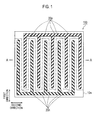
- Fig. 1 is a plan view of the back surface side of the solar cell 100 according to the first embodiment.
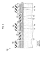
- Fig. 2 is an enlarged cross-sectional view along the A-A line of Fig. 1 .
- the solar cell 100 includes an n-type crystalline silicon substrate 10n, an i-type amorphous semiconductor layer 11i, a p-type amorphous semiconductor layer 11p, an i-type amorphous semiconductor layer 12i, an n-type amorphous semiconductor layer 12n, p-side electrodes 20p and n-side electrodes 20n.
- the n-type crystalline silicon substrate 10n is formed of thin plate-shaped monocrystalline silicon or polycrystalline silicon.
- the n-type crystalline silicon substrate 10n has a light-receiving surface to receive sunlight, and a back surface provided on a side opposite to the light-receiving surface.
- the n-type crystalline silicon substrate 10n generates photogenerated carriers by the light received on the light-receiving surface.
- the photogenerated carrier includes an electron and a hole produced when light is absorbed into the n-type crystalline silicon substrate 10n.
- a structure e.g., an electrode
- light can be received on the entire light receiving surface.
- the i-type amorphous semiconductor layer 11i is formed along a first direction on the back surface of the n-type crystalline silicon substrate 10n.
- the i-type amorphous semiconductor layer 11i is formed without actively introducing an impurity.
- the i-type amorphous semiconductor layer 11i has a thickness not to practically contribute to the generation of electricity, e.g., a thickness of about several ⁇ to 250 ⁇ .
- the p-type amorphous semiconductor layer 11p is formed along the first direction on the i-type amorphous semiconductor layer 11i.
- the p-type amorphous semiconductor layer 11p has p-type conductivity.
- the p-type amorphous semiconductor layer 11p has a thickness of about 10 nm, for example.
- the i-type amorphous semiconductor layer 11i may not be formed, but is preferably formed because the structure in which the i-type amorphous semiconductor layer 11i and the p-type amorphous semiconductor layer 11p are formed in this order on the n-type crystalline silicon substrate 10n (so called, "HIT structure”) can improve the p-n junction characteristics.
- the i-type amorphous semiconductor layer 12i is formed on the back surface of the n-type crystalline silicon substrate 10n and also on the p-type amorphous semiconductor layer 11p.
- the i-type amorphous semiconductor layer 12i is formed so as to cover substantially the entire back surface of the n-type crystalline silicon substrate 10n.
- the i-type amorphous semiconductor layer 12i is formed without active introduction of impurities.
- the i-type amorphous semiconductor layer 12i has a thickness of about several ⁇ to 250 ⁇ , for example.
- the n-type amorphous semiconductor layer 12n is formed on the i-type amorphous semiconductor layer 12i.
- the n-type amorphous semiconductor layer 12n is formed so as to cover the i-type amorphous semiconductor layer 12i.
- the n-type amorphous semiconductor layer 12n has n-type conductivity different from the conductivity type of the p-type amorphous semiconductor layer 11p.
- the n-type amorphous semiconductor layer 12n has a thickness of about 10 nm, for example.
- the structure in which the n-type amorphous semiconductor layer 12n is formed above the n-type crystalline silicon substrate 10n makes it possible to prevent recombination of minority carriers in the boundary between the back surface of the n-type crystalline silicon substrate 10n and the amorphous semiconductor layer.
- the structure in which the thin i-type amorphous semiconductor layer 12i is inserted between the back surface of the n-type crystalline silicon substrate 10n and the n-type amorphous semiconductor layer 12n makes an improvement in the characteristics of a portion between the back surface of the n-type crystalline silicon substrate 10n and the n-type amorphous semiconductor layer 12n.
- each of the i-type amorphous semiconductor layer 11i, the i-type amorphous semiconductor layer 12i, the p-type amorphous semiconductor layer 11p and the n-type amorphous semiconductor layer 12n can be formed of an amorphous semiconductor containing silicon.
- the amorphous semiconductor containing silicon include amorphous silicon, amorphous silicon carbide, amorphous silicon germanium and the like, but the amorphous semiconductor containing silicon is not limited to these examples, and other amorphous semiconductor can be used as well.
- each of the i-type amorphous semiconductor layer 11i, the i-type amorphous semiconductor layer 12i, the p-type amorphous semiconductor layer 11p and the n-type amorphous semiconductor layer 12n may be formed of amorphous semiconductor of one kind or a combination of amorphous semiconductor of two or more kinds.
- the p-side electrodes 20p each are a collecting electrode configured to collect carriers.
- the p-side electrodes 20p are formed above the p-type amorphous semiconductor layer 11p across the i-type amorphous semiconductor layer 12i and the n-type amorphous semiconductor layer 12n. Accordingly, the p-side electrodes 20p are each formed in a line shape along the first direction.
- the n-side electrodes 20n are each a collecting electrode configured to collect carriers.
- the n-side electrodes 20n are formed above the back surface of the n-type crystalline silicon substrate 10n across the i-type amorphous semiconductor layer 12i and the n-type amorphous semiconductor layer 12n. Accordingly, the n-side electrodes 20n are each formed in a line shape along the first direction between one of the p-side electrodes 20p and another one of the p-side electrodes 20p.
- the n-side electrodes 20n and the p-side electrodes 20p may be each formed in a single-layered structure or a multilayered structure.
- a transparent conductive layer may be provided on a side close to the n-type amorphous semiconductor layer 12n.
- a transparent conductive oxide such as indium oxide, tin oxide or zinc oxide or the like can be used, for example.
- the n-side electrodes 20n and the p-side electrodes 20p may be each formed to substantially cover the entire surface of a corresponding one of the p-type amorphous semiconductor layer 11p or the n-type amorphous semiconductor layer 12n.
- the p-side electrodes 20p and the n-side electrodes 20n can adequately collect carriers.
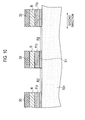
- the i-type amorphous semiconductor layer 11i and the p-type amorphous semiconductor layer 11p are formed in this order on the entire back surface of the n-type crystalline silicon substrate 10n by use of a CVD method.
- a resist film 30 is applied onto the p-type amorphous semiconductor layer 11p in a predetermined pattern.
- the predetermined pattern corresponds to regions where the p-side electrodes 20p are to be formed.
- the predetermined pattern is set along a dashed-dotted line of FIG. 1 as the basis, for example.
- a wet etching process is performed for removal of exposed regions R1 of the i-type amorphous semiconductor layer 11i and the p-type amorphous semiconductor layer 11p, which are exposed from the resist film 30.
- the i-type amorphous semiconductor layer 11i and the p-type amorphous semiconductor layer 11p are patterned.
- a wet etching process and a hydrogen plasma process are performed for cleaning exposed regions R2 of the back surface of the n-type crystalline silicon substrate 10n, which are the exposed regions thereof.
- the amount of the wet etching process and the hydrogen plasma process applied onto the surface of the p-type amorphous semiconductor layer 11p is preferably set to be small in this case.
- the i-type amorphous semiconductor layer 12i and the n-type amorphous semiconductor layer 12n are formed in this order by use of a CVD method on the back surface of the n-type crystalline silicon substrate 10n and also on the p-type amorphous semiconductor layer 11p.
- the p-side electrodes 20p and the n-side electrodes 20n are formed in a predetermined pattern on the n-type amorphous semiconductor layer 12n by use of a CVD method, a sputtering method, a vapor deposition method, a plating method or a printing method or the like.
- the method of manufacturing the solar cell 100 according to the first embodiment includes the step of cleaning the exposed regions R2 of the back surface of n-type crystalline silicon substrate 10n after the step of patterning the i-type amorphous semiconductor layer 11i and the p-type amorphous semiconductor layer 11p but before the step of forming the i-type amorphous semiconductor layer 12i.
- this method can prevent recombination of carriers in the boundary between the back surface of the n-type crystalline silicon substrate 10n and the i-type amorphous semiconductor layer 12i.
- the i-type amorphous semiconductor layer 12i and the n-type amorphous semiconductor layer 12n are formed in this order after the step of cleaning the exposed regions R2 in the method of manufacturing the solar cell 100 according to the first embodiment.
- the i-type amorphous semiconductor layer 12i and the n-type amorphous semiconductor layer 12n do not have to be patterned by a mask or the like. For this reason, the productivity of the solar cell 100 can be improved.
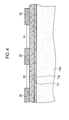
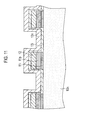
- the solar cell 100 according to the second embodiment includes a recombination layer R inserted between the p-type amorphous semiconductor layer 11p and the i-type amorphous semiconductor layer 12i.
- FIG. 7 is a cross-sectional view of the solar cell 100 according to the second embodiment.
- the solar cell 100 includes the recombination layer R on the p-type amorphous semiconductor layer 11p.
- the recombination layer R is provided for the purpose of preventing the p-type amorphous semiconductor layer 11p, the i-type amorphous semiconductor layer 12i and the n-type amorphous semiconductor layer 12n from forming an electric field in a direction opposite to an electric field formed by the n-type crystalline silicon substrate 10n, the i-type amorphous semiconductor layer 11i and the p-type amorphous semiconductor layer 11p.
- a reduction in the resistance between the p-side electrodes 20p and the p-type amorphous semiconductor layer 11p is achieved by insertion of the recombination layer R in this embodiment.
- the thickness of the recombination layer R is preferably 0.1 to 20 nm, or more preferably, 1 to 10 nm.
- the recombination layer R having the aforementioned characteristics is formed of (1) a semiconductor material in which a large number of in-gap states existing in an energy band exist, or (2) a metal material that forms an ohmic contact with the p-type amorphous semiconductor layer 11p.
- the carriers generated in the n-type crystalline silicon substrate 10n via the p-type amorphous semiconductor layer 11p can be extracted by utilizing recombination of carriers via a large number of in-gap states in an energy band. Accordingly, even when the recombination layer R is formed on the surface of the p-type amorphous semiconductor layer 11p, the contact between the both layers has a low resistance, i.e., comes near an ohmic contact.
- the thickness of the i-type amorphous semiconductor layer 12i formed on the surface of the recombination layer R is extremely thin, the function thereof as a barrier wall against the carriers is extremely small.
- the carriers can be extracted through the p-side electrodes 20p in a good state.
- the semiconductor material forming the recombination layer R it is possible to use (i) a semiconductor material containing a large amount of impurities or (ii) a semiconductor material containing a large number of lattice defects. Note that, it is also possible to use a p-type semiconductor material containing a larger amount of p-type impurities than the p-type amorphous semiconductor layer 11p, or, as the material described in (i), a p-type semiconductor material containing a larger amount of p-type impurities than the p-type amorphous semiconductor layer 11p, or an n-type semiconductor material containing a larger amount of n-type impurities than the n-type amorphous semiconductor layer 12n or the like.
- the material described in (ii) it is possible to use a semiconductor material in which lattice defects are increased by mixing an element of a different kind such as carbon or germanium in amorphous silicon (amorphous silicon carbide or amorphous silicon germanium), or p-type or n-type microcrystalline silicon or the like, for example.
- amorphous silicon amorphous silicon carbide or amorphous silicon germanium
- p-type or n-type microcrystalline silicon or the like for example.
- the conductivity type of the recombination layer R is p-type, it is possible to suppress an increase in the manufacturing costs because the recombination layer R can be formed by use of the same raw material gas as that for the amorphous semiconductor layer 12p.
- the contact between the both layers has a low resistance, i.e., comes near an ohmic contact. Accordingly, since a reduction in the resistance between the p-side electrodes 20p and the p-type amorphous semiconductor layer 11p is achieved, the carriers can be extracted through the p-side electrodes 20p in a good state.
- titanium (Ti) or tungsten (W) or the like can be used as the metal material described above.
- the recombination layer R is formed after the i-type amorphous semiconductor layer 11i and the p-type amorphous semiconductor layer 11p are formed in this order on the entire back surface of the n-type crystalline silicon substrate 10n by use of a CVD method.
- a CVD method or the like is used.
- a sputtering method or a vapor deposition method can be used.
- a resist film 30 is applied onto the recombination layer R in a predetermined pattern.
- the predetermined pattern corresponds to regions where the p-side electrodes 20p are formed.
- the predetermined pattern is set along a dashed-dotted line of FIG. 1 as the basis, for example.
- a wet etching process is performed for removal of exposed regions R1 of the i-type amorphous semiconductor layer 11i, the p-type amorphous semiconductor layer 11p and the recombination layer R, which are exposed from the resist film 30.
- the i-type amorphous semiconductor layer 11i, the p-type amorphous semiconductor layer 11p and the recombination layer R are patterned.
- a wet etching process and a hydrogen plasma process are performed for cleaning exposed regions R2 of the back surface of the n-type crystalline silicon substrate 10n, which are the exposed regions thereof. During this cleaning, the wet etching process and the hydrogen plasma process may be performed on the recombination layer R as well.
- the i-type amorphous semiconductor layer 12i and the n-type amorphous semiconductor layer 12n are formed in this order by use a CVD method on the back surface of the n-type crystalline silicon substrate 10n and also on the recombination layer R.
- the p-side electrodes 20p and the n-side electrodes 20n are formed in a predetermined pattern on the n-type amorphous semiconductor layer 12n by use of a CVD method, a sputtering method, a vapor deposition method, a plating method or a printing method or the like.
- the method of manufacturing the solar cell 100 according to the second embodiment includes the step of forming the recombination layer R on the p-type amorphous semiconductor layer 11p.
- the i-type amorphous semiconductor layer 12i and the n-type amorphous semiconductor layer 12n are formed in this order on the back surface of the n-type crystalline silicon substrate 10n and also on the recombination layer R.
- the solar cell 100 has the recombination layer R inserted between the p-type amorphous semiconductor layer 11p and the n-type amorphous semiconductor layer 12n.
- the p-type amorphous semiconductor layer 11p and the recombination layer R are in contact with each other with a low resistance.
- the p-type amorphous semiconductor layer 11p, the i-type amorphous semiconductor layer 12i and the n-type amorphous semiconductor layer 12n can be prevented from forming an electric field in a direction opposite to an electric field formed by the n-type crystalline silicon substrate 10n, the i-type amorphous semiconductor layer 11i and the p-type amorphous semiconductor layer 11p.
- a reduction in the resistance between the p-side electrodes 20p and the p-type amorphous semiconductor layer 11p is achieved. Accordingly, the carriers can be extracted through the p-side electrodes 20p in a good state. As a result, a carrier collection loss can be reduced. Thus, it is possible to improve the characteristics of the solar cell 100.
- the n-type crystalline silicon substrate 10n is used as the substrate of the solar cell 100, but the substrate of the solar cell 100 is not limited to this.
- the substrate of the solar cell 100 may have p-type conductivity, for example.
- the substrate of the solar cell 100 may be formed of a crystalline semiconductor material such as polycrystalline Si, microcrystalline Si or the like, or a general semiconductor material including a compound semiconductor material such as GaAs, InP or the like.
- the p-type amorphous semiconductor layer 11p is formed on the back surface of the n-type crystalline silicon substrate 10n, and the n-type amorphous semiconductor layer 12n is formed thereafter in the aforementioned embodiments, but the formation sequence is not limited to this.
- the formation sequence of the p-type amorphous semiconductor layer 11p and the n-type amorphous semiconductor layer 12n may be reversed, for example.
- the p-type amorphous semiconductor layer 11p may be formed after the n-type amorphous semiconductor layer 12n is formed on the back surface of the n-type crystalline silicon substrate 10n.
- the p-type amorphous semiconductor layer 11p and the n-type amorphous semiconductor layer 12n are preferably formed in positions reverse to the positions in the aforementioned embodiments when a p-type substrate is used.
- the n-type amorphous semiconductor layer 12n is formed to cover the i-type amorphous semiconductor layer 11i.
- a leakage between the p-side electrodes 20p and the n-side electrodes 20n is more likely to be prevented from occurring because n-type amorphous silicon has a larger electric resistance than p-type amorphous silicon in general.
- the i-type amorphous semiconductor layer 11i and the i-type amorphous semiconductor layer 12i are formed without active introduction of impurities in the aforementioned embodiments, but the i-type amorphous semiconductor layer 11i and the i-type amorphous semiconductor layer 12i may contain a slight amount of dopant.
- the i-type amorphous semiconductor layer 13i may not be formed on the back surface of the n-type crystalline silicon substrate 10n. In this case, the resistance of the back surface side of the n-type crystalline silicon substrate 10n can be further reduced.
- the recombination layer R is configured of a single layer structure in the aforementioned embodiments, but is not limited to this configuration.
- the recombination layer R may be configured of a structure further including another layer capable of keeping an ohmic contact with the p-type amorphous semiconductor layer 11p.
- the p-type amorphous semiconductor layer 11p is configured of a single layer structure in the aforementioned embodiments, but is not limited to this configuration.
- the p-type amorphous semiconductor layer 11p may be configured of a structure further including another layer capable of keeping an ohmic contact with the recombination layer R.
- the method of manufacturing a solar cell according to the present invention is useful in the production field of solar cells because a solar cell capable of preventing recombination of carriers can be provided.
Landscapes
- Photovoltaic Devices (AREA)
- Weting (AREA)
Applications Claiming Priority (2)
| Application Number | Priority Date | Filing Date | Title |
|---|---|---|---|
| JP2009044435A JP5518347B2 (ja) | 2009-02-26 | 2009-02-26 | 太陽電池の製造方法 |
| PCT/JP2010/053087 WO2010098446A1 (ja) | 2009-02-26 | 2010-02-26 | 太陽電池の製造方法 |
Publications (2)
| Publication Number | Publication Date |
|---|---|
| EP2403005A1 true EP2403005A1 (de) | 2012-01-04 |
| EP2403005A4 EP2403005A4 (de) | 2013-10-23 |
Family
ID=42665650
Family Applications (1)
| Application Number | Title | Priority Date | Filing Date |
|---|---|---|---|
| EP10746325.9A Ceased EP2403005A4 (de) | 2009-02-26 | 2010-02-26 | Verfahren zur herstellung von solarzellen |
Country Status (5)
| Country | Link |
|---|---|
| US (1) | US8664034B2 (de) |
| EP (1) | EP2403005A4 (de) |
| JP (1) | JP5518347B2 (de) |
| CN (1) | CN102334192A (de) |
| WO (1) | WO2010098446A1 (de) |
Cited By (1)
| Publication number | Priority date | Publication date | Assignee | Title |
|---|---|---|---|---|
| DE112012006605B4 (de) | 2012-06-29 | 2021-10-14 | Panasonic Intellectual Property Management Co., Ltd. | Solarzelle |
Families Citing this family (10)
| Publication number | Priority date | Publication date | Assignee | Title |
|---|---|---|---|---|
| JPWO2012132834A1 (ja) * | 2011-03-28 | 2014-07-28 | 三洋電機株式会社 | 太陽電池及び太陽電池の製造方法 |
| WO2013002008A1 (ja) * | 2011-06-29 | 2013-01-03 | 三洋電機株式会社 | 太陽電池 |
| JP6032911B2 (ja) * | 2012-03-23 | 2016-11-30 | シャープ株式会社 | 光電変換素子およびその製造方法 |
| US9640676B2 (en) * | 2012-06-29 | 2017-05-02 | Sunpower Corporation | Methods and structures for improving the structural integrity of solar cells |
| DE112012006595T5 (de) * | 2012-06-29 | 2015-04-02 | Sanyo Electric Co., Ltd. | Solarzelle |
| JP2014075526A (ja) * | 2012-10-05 | 2014-04-24 | Sharp Corp | 光電変換素子および光電変換素子の製造方法 |
| EP3223318A1 (de) | 2016-03-23 | 2017-09-27 | Meyer Burger (Germany) AG | Heteroübergangs-photovoltaikzelle und verfahren zur herstellung davon |
| WO2017164099A1 (ja) * | 2016-03-23 | 2017-09-28 | シャープ株式会社 | 光電変換装置、光電変換モジュールおよび太陽光発電システム |
| WO2020149128A1 (ja) * | 2019-01-18 | 2020-07-23 | 株式会社カネカ | 太陽電池の製造方法 |
| JP7526086B2 (ja) * | 2020-12-21 | 2024-07-31 | 株式会社カネカ | 太陽電池の製造方法、および製膜方法 |
Family Cites Families (9)
| Publication number | Priority date | Publication date | Assignee | Title |
|---|---|---|---|---|
| JPH11354820A (ja) * | 1998-06-12 | 1999-12-24 | Sharp Corp | 光電変換素子及びその製造方法 |
| JP2002280584A (ja) * | 2001-03-19 | 2002-09-27 | Kanegafuchi Chem Ind Co Ltd | ハイブリッド型薄膜光電変換装置とその製造方法 |
| JP3998619B2 (ja) * | 2003-09-24 | 2007-10-31 | 三洋電機株式会社 | 光起電力素子およびその製造方法 |
| CN100431177C (zh) * | 2003-09-24 | 2008-11-05 | 三洋电机株式会社 | 光生伏打元件及其制造方法 |
| FR2880989B1 (fr) * | 2005-01-20 | 2007-03-09 | Commissariat Energie Atomique | Dispositif semi-conducteur a heterojonctions et a structure inter-digitee |
| US20080000522A1 (en) | 2006-06-30 | 2008-01-03 | General Electric Company | Photovoltaic device which includes all-back-contact configuration; and related processes |
| JP2009152222A (ja) * | 2006-10-27 | 2009-07-09 | Kyocera Corp | 太陽電池素子の製造方法 |
| JP2009044435A (ja) | 2007-08-08 | 2009-02-26 | Toshiba Corp | 放送/vod受信装置と視聴管理方法 |
| US20110000532A1 (en) | 2008-01-30 | 2011-01-06 | Kyocera Corporation | Solar Cell Device and Method of Manufacturing Solar Cell Device |
-
2009
- 2009-02-26 JP JP2009044435A patent/JP5518347B2/ja not_active Expired - Fee Related
-
2010
- 2010-02-26 US US13/203,509 patent/US8664034B2/en active Active
- 2010-02-26 CN CN2010800092234A patent/CN102334192A/zh active Pending
- 2010-02-26 EP EP10746325.9A patent/EP2403005A4/de not_active Ceased
- 2010-02-26 WO PCT/JP2010/053087 patent/WO2010098446A1/ja not_active Ceased
Cited By (1)
| Publication number | Priority date | Publication date | Assignee | Title |
|---|---|---|---|---|
| DE112012006605B4 (de) | 2012-06-29 | 2021-10-14 | Panasonic Intellectual Property Management Co., Ltd. | Solarzelle |
Also Published As
| Publication number | Publication date |
|---|---|
| EP2403005A4 (de) | 2013-10-23 |
| WO2010098446A1 (ja) | 2010-09-02 |
| JP5518347B2 (ja) | 2014-06-11 |
| JP2010199416A (ja) | 2010-09-09 |
| CN102334192A (zh) | 2012-01-25 |
| US20120052622A1 (en) | 2012-03-01 |
| US8664034B2 (en) | 2014-03-04 |
Similar Documents
| Publication | Publication Date | Title |
|---|---|---|
| EP2403004B1 (de) | Solarzelle | |
| US8664034B2 (en) | Method of manufacturing solar cell | |
| US9006564B2 (en) | Method of manufacturing solar cell and solar cell | |
| EP2530729B1 (de) | Solarzelle und herstellungsverfahren dafür | |
| KR101826912B1 (ko) | 광전변환소자 및 그 제조 방법 | |
| EP3170209B1 (de) | Solarzelle mit verfingertem rückseitenkontakt | |
| EP2541617B1 (de) | Solarzelle und verfahren zur herstellung einer solarzelle | |
| KR101521326B1 (ko) | 태양 전지 | |
| US12610653B2 (en) | Solar cell, preparation method thereof and photovoltaic module | |
| US20130288423A1 (en) | Method of manufacturing solar cell and solar cell | |
| US20120325309A1 (en) | Solar cell and solar cell manufacturing method | |
| CN101632180A (zh) | 混合硅太阳电池及其制造方法 | |
| US20130180585A1 (en) | Method of manufacturing solar cell, and solar cell | |
| KR101985835B1 (ko) | 광기전력소자 및 제조 방법 | |
| US20190386160A1 (en) | Solar cell | |
| US20170117433A1 (en) | A hybrid all-back-contact solar cell and method of fabricating the same | |
| JP2008085374A (ja) | 光起電力素子 | |
| JP5645734B2 (ja) | 太陽電池素子 | |
| JP4945916B2 (ja) | 光電変換素子 | |
| KR101103706B1 (ko) | 후면접합 태양전지의 제조방법 | |
| CN117995923A (zh) | 太阳能电池的形成方法、太阳能电池及光伏组件 | |
| EP2690669A1 (de) | Solarzelle | |
| JP5816800B2 (ja) | 太陽電池の製造方法 |
Legal Events
| Date | Code | Title | Description |
|---|---|---|---|
| PUAI | Public reference made under article 153(3) epc to a published international application that has entered the european phase |
Free format text: ORIGINAL CODE: 0009012 |
|
| 17P | Request for examination filed |
Effective date: 20110909 |
|
| AK | Designated contracting states |
Kind code of ref document: A1 Designated state(s): AT BE BG CH CY CZ DE DK EE ES FI FR GB GR HR HU IE IS IT LI LT LU LV MC MK MT NL NO PL PT RO SE SI SK SM TR |
|
| DAX | Request for extension of the european patent (deleted) | ||
| A4 | Supplementary search report drawn up and despatched |
Effective date: 20130923 |
|
| RIC1 | Information provided on ipc code assigned before grant |
Ipc: H01L 31/0747 20120101ALI20130917BHEP Ipc: H01L 31/068 20120101ALI20130917BHEP Ipc: H01L 31/04 20060101AFI20130917BHEP Ipc: H01L 31/18 20060101ALI20130917BHEP Ipc: H01L 31/0224 20060101ALI20130917BHEP |
|
| 17Q | First examination report despatched |
Effective date: 20151019 |
|
| RAP1 | Party data changed (applicant data changed or rights of an application transferred) |
Owner name: PANASONIC INTELLECTUAL PROPERTY MANAGEMENT CO., LT |
|
| REG | Reference to a national code |
Ref country code: DE Ref legal event code: R003 |
|
| STAA | Information on the status of an ep patent application or granted ep patent |
Free format text: STATUS: THE APPLICATION HAS BEEN REFUSED |
|
| 18R | Application refused |
Effective date: 20171107 |