EP2541617B1 - Solarzelle und verfahren zur herstellung einer solarzelle - Google Patents
Solarzelle und verfahren zur herstellung einer solarzelle Download PDFInfo
- Publication number
- EP2541617B1 EP2541617B1 EP11747510.3A EP11747510A EP2541617B1 EP 2541617 B1 EP2541617 B1 EP 2541617B1 EP 11747510 A EP11747510 A EP 11747510A EP 2541617 B1 EP2541617 B1 EP 2541617B1
- Authority
- EP
- European Patent Office
- Prior art keywords
- semiconductor layer
- layer
- semiconductor
- solar cell
- insulating
- Prior art date
- Legal status (The legal status is an assumption and is not a legal conclusion. Google has not performed a legal analysis and makes no representation as to the accuracy of the status listed.)
- Not-in-force
Links
- 238000000034 method Methods 0.000 title claims description 49
- 238000004519 manufacturing process Methods 0.000 title claims description 31
- 239000004065 semiconductor Substances 0.000 claims description 354
- 239000000758 substrate Substances 0.000 claims description 61
- 238000002955 isolation Methods 0.000 claims description 56
- 230000015572 biosynthetic process Effects 0.000 claims description 32
- 238000009413 insulation Methods 0.000 claims description 6
- 238000002161 passivation Methods 0.000 claims description 5
- 239000000969 carrier Substances 0.000 description 29
- 238000005215 recombination Methods 0.000 description 10
- 230000006798 recombination Effects 0.000 description 10
- 239000000463 material Substances 0.000 description 7
- 238000006243 chemical reaction Methods 0.000 description 5
- 238000005229 chemical vapour deposition Methods 0.000 description 4
- 229910021417 amorphous silicon Inorganic materials 0.000 description 3
- 238000004140 cleaning Methods 0.000 description 3
- 229910052751 metal Inorganic materials 0.000 description 3
- 239000002184 metal Substances 0.000 description 3
- 238000005240 physical vapour deposition Methods 0.000 description 3
- 238000007650 screen-printing Methods 0.000 description 3
- BQCADISMDOOEFD-UHFFFAOYSA-N Silver Chemical compound [Ag] BQCADISMDOOEFD-UHFFFAOYSA-N 0.000 description 2
- XLOMVQKBTHCTTD-UHFFFAOYSA-N Zinc monoxide Chemical compound [Zn]=O XLOMVQKBTHCTTD-UHFFFAOYSA-N 0.000 description 2
- 239000002019 doping agent Substances 0.000 description 2
- 230000000694 effects Effects 0.000 description 2
- 238000005530 etching Methods 0.000 description 2
- 229910021421 monocrystalline silicon Inorganic materials 0.000 description 2
- 239000002245 particle Substances 0.000 description 2
- 238000000206 photolithography Methods 0.000 description 2
- 238000007747 plating Methods 0.000 description 2
- 230000001681 protective effect Effects 0.000 description 2
- 239000011347 resin Substances 0.000 description 2
- 229920005989 resin Polymers 0.000 description 2
- 229910052709 silver Inorganic materials 0.000 description 2
- 239000004332 silver Substances 0.000 description 2
- KRHYYFGTRYWZRS-UHFFFAOYSA-N Fluorane Chemical compound F KRHYYFGTRYWZRS-UHFFFAOYSA-N 0.000 description 1
- 229910001218 Gallium arsenide Inorganic materials 0.000 description 1
- UFHFLCQGNIYNRP-UHFFFAOYSA-N Hydrogen Chemical compound [H][H] UFHFLCQGNIYNRP-UHFFFAOYSA-N 0.000 description 1
- 229910052581 Si3N4 Inorganic materials 0.000 description 1
- VYPSYNLAJGMNEJ-UHFFFAOYSA-N Silicium dioxide Chemical compound O=[Si]=O VYPSYNLAJGMNEJ-UHFFFAOYSA-N 0.000 description 1
- LEVVHYCKPQWKOP-UHFFFAOYSA-N [Si].[Ge] Chemical compound [Si].[Ge] LEVVHYCKPQWKOP-UHFFFAOYSA-N 0.000 description 1
- 239000002253 acid Substances 0.000 description 1
- 239000003513 alkali Substances 0.000 description 1
- 239000012670 alkaline solution Substances 0.000 description 1
- 239000011230 binding agent Substances 0.000 description 1
- 150000001875 compounds Chemical class 0.000 description 1
- 239000004020 conductor Substances 0.000 description 1
- 239000000356 contaminant Substances 0.000 description 1
- 229910052802 copper Inorganic materials 0.000 description 1
- PMHQVHHXPFUNSP-UHFFFAOYSA-M copper(1+);methylsulfanylmethane;bromide Chemical compound Br[Cu].CSC PMHQVHHXPFUNSP-UHFFFAOYSA-M 0.000 description 1
- 239000013078 crystal Substances 0.000 description 1
- 230000007423 decrease Effects 0.000 description 1
- 230000006866 deterioration Effects 0.000 description 1
- 239000000945 filler Substances 0.000 description 1
- 229910052739 hydrogen Inorganic materials 0.000 description 1
- 239000001257 hydrogen Substances 0.000 description 1
- AMGQUBHHOARCQH-UHFFFAOYSA-N indium;oxotin Chemical compound [In].[Sn]=O AMGQUBHHOARCQH-UHFFFAOYSA-N 0.000 description 1
- 150000002739 metals Chemical class 0.000 description 1
- 229910021420 polycrystalline silicon Inorganic materials 0.000 description 1
- 230000005855 radiation Effects 0.000 description 1
- HBMJWWWQQXIZIP-UHFFFAOYSA-N silicon carbide Chemical compound [Si+]#[C-] HBMJWWWQQXIZIP-UHFFFAOYSA-N 0.000 description 1
- HQVNEWCFYHHQES-UHFFFAOYSA-N silicon nitride Chemical compound N12[Si]34N5[Si]62N3[Si]51N64 HQVNEWCFYHHQES-UHFFFAOYSA-N 0.000 description 1
- 229910052814 silicon oxide Inorganic materials 0.000 description 1
- 238000005245 sintering Methods 0.000 description 1
- 238000004544 sputter deposition Methods 0.000 description 1
- XOLBLPGZBRYERU-UHFFFAOYSA-N tin dioxide Chemical compound O=[Sn]=O XOLBLPGZBRYERU-UHFFFAOYSA-N 0.000 description 1
- 229910001887 tin oxide Inorganic materials 0.000 description 1
- 239000011787 zinc oxide Substances 0.000 description 1
Images




Classifications
-
- H—ELECTRICITY
- H10—SEMICONDUCTOR DEVICES; ELECTRIC SOLID-STATE DEVICES NOT OTHERWISE PROVIDED FOR
- H10F—INORGANIC SEMICONDUCTOR DEVICES SENSITIVE TO INFRARED RADIATION, LIGHT, ELECTROMAGNETIC RADIATION OF SHORTER WAVELENGTH OR CORPUSCULAR RADIATION
- H10F77/00—Constructional details of devices covered by this subclass
- H10F77/20—Electrodes
- H10F77/206—Electrodes for devices having potential barriers
- H10F77/211—Electrodes for devices having potential barriers for photovoltaic cells
- H10F77/219—Arrangements for electrodes of back-contact photovoltaic cells
-
- H—ELECTRICITY
- H10—SEMICONDUCTOR DEVICES; ELECTRIC SOLID-STATE DEVICES NOT OTHERWISE PROVIDED FOR
- H10F—INORGANIC SEMICONDUCTOR DEVICES SENSITIVE TO INFRARED RADIATION, LIGHT, ELECTROMAGNETIC RADIATION OF SHORTER WAVELENGTH OR CORPUSCULAR RADIATION
- H10F10/00—Individual photovoltaic cells, e.g. solar cells
- H10F10/10—Individual photovoltaic cells, e.g. solar cells having potential barriers
- H10F10/14—Photovoltaic cells having only PN homojunction potential barriers
- H10F10/146—Back-junction photovoltaic cells, e.g. having interdigitated base-emitter regions on the back side
-
- H—ELECTRICITY
- H10—SEMICONDUCTOR DEVICES; ELECTRIC SOLID-STATE DEVICES NOT OTHERWISE PROVIDED FOR
- H10F—INORGANIC SEMICONDUCTOR DEVICES SENSITIVE TO INFRARED RADIATION, LIGHT, ELECTROMAGNETIC RADIATION OF SHORTER WAVELENGTH OR CORPUSCULAR RADIATION
- H10F10/00—Individual photovoltaic cells, e.g. solar cells
- H10F10/10—Individual photovoltaic cells, e.g. solar cells having potential barriers
- H10F10/16—Photovoltaic cells having only PN heterojunction potential barriers
- H10F10/164—Photovoltaic cells having only PN heterojunction potential barriers comprising heterojunctions with Group IV materials, e.g. ITO/Si or GaAs/SiGe photovoltaic cells
- H10F10/165—Photovoltaic cells having only PN heterojunction potential barriers comprising heterojunctions with Group IV materials, e.g. ITO/Si or GaAs/SiGe photovoltaic cells the heterojunctions being Group IV-IV heterojunctions, e.g. Si/Ge, SiGe/Si or Si/SiC photovoltaic cells
- H10F10/166—Photovoltaic cells having only PN heterojunction potential barriers comprising heterojunctions with Group IV materials, e.g. ITO/Si or GaAs/SiGe photovoltaic cells the heterojunctions being Group IV-IV heterojunctions, e.g. Si/Ge, SiGe/Si or Si/SiC photovoltaic cells the Group IV-IV heterojunctions being heterojunctions of crystalline and amorphous materials, e.g. silicon heterojunction [SHJ] photovoltaic cells
-
- H—ELECTRICITY
- H10—SEMICONDUCTOR DEVICES; ELECTRIC SOLID-STATE DEVICES NOT OTHERWISE PROVIDED FOR
- H10F—INORGANIC SEMICONDUCTOR DEVICES SENSITIVE TO INFRARED RADIATION, LIGHT, ELECTROMAGNETIC RADIATION OF SHORTER WAVELENGTH OR CORPUSCULAR RADIATION
- H10F71/00—Manufacture or treatment of devices covered by this subclass
- H10F71/121—The active layers comprising only Group IV materials
-
- H—ELECTRICITY
- H10—SEMICONDUCTOR DEVICES; ELECTRIC SOLID-STATE DEVICES NOT OTHERWISE PROVIDED FOR
- H10F—INORGANIC SEMICONDUCTOR DEVICES SENSITIVE TO INFRARED RADIATION, LIGHT, ELECTROMAGNETIC RADIATION OF SHORTER WAVELENGTH OR CORPUSCULAR RADIATION
- H10F71/00—Manufacture or treatment of devices covered by this subclass
- H10F71/138—Manufacture of transparent electrodes, e.g. transparent conductive oxides [TCO] or indium tin oxide [ITO] electrodes
-
- Y—GENERAL TAGGING OF NEW TECHNOLOGICAL DEVELOPMENTS; GENERAL TAGGING OF CROSS-SECTIONAL TECHNOLOGIES SPANNING OVER SEVERAL SECTIONS OF THE IPC; TECHNICAL SUBJECTS COVERED BY FORMER USPC CROSS-REFERENCE ART COLLECTIONS [XRACs] AND DIGESTS
- Y02—TECHNOLOGIES OR APPLICATIONS FOR MITIGATION OR ADAPTATION AGAINST CLIMATE CHANGE
- Y02E—REDUCTION OF GREENHOUSE GAS [GHG] EMISSIONS, RELATED TO ENERGY GENERATION, TRANSMISSION OR DISTRIBUTION
- Y02E10/00—Energy generation through renewable energy sources
- Y02E10/50—Photovoltaic [PV] energy
- Y02E10/547—Monocrystalline silicon PV cells
-
- Y—GENERAL TAGGING OF NEW TECHNOLOGICAL DEVELOPMENTS; GENERAL TAGGING OF CROSS-SECTIONAL TECHNOLOGIES SPANNING OVER SEVERAL SECTIONS OF THE IPC; TECHNICAL SUBJECTS COVERED BY FORMER USPC CROSS-REFERENCE ART COLLECTIONS [XRACs] AND DIGESTS
- Y02—TECHNOLOGIES OR APPLICATIONS FOR MITIGATION OR ADAPTATION AGAINST CLIMATE CHANGE
- Y02P—CLIMATE CHANGE MITIGATION TECHNOLOGIES IN THE PRODUCTION OR PROCESSING OF GOODS
- Y02P70/00—Climate change mitigation technologies in the production process for final industrial or consumer products
- Y02P70/50—Manufacturing or production processes characterised by the final manufactured product
Definitions
- the invention relates to a solar cell of a rear junction type in which an n-type semiconductor layer and a p-type semiconductor layer are formed on a rear surface of a semiconductor substrate and also relates to a method for manufacturing the solar cell.
- a solar cell can convert clean and unlimitedly-supplied solar energy directly into electric energy and is therefore expected to be a new energy source.
- Patent Document 1 A solar cell in which an n-type semiconductor layer and a p-type semiconductor layer are formed on a rear surface of a semiconductor substrate, or a so-called rear junction type solar cell, has been conventionally known (For example, Patent Document 1).
- Fig. 1 is a cross-sectional view of conventional rear junction type solar cell 100.
- n-type semiconductor layer 120 and p-type semiconductor layer 130 are formed on a rear surface of n-type semiconductor substrate 110.
- Insulating layer 140 is formed to be laid on n-type semiconductor layer 120 and p-type semiconductor layer 130. Short circuit between p-side electrode 150p and n-side electrode 150n is prevented by forming isolation grooves 160 for p-side electrodes 150p and n-side electrodes 150n on insulating layer 140.
- carriers are generated in semiconductor substrate 110 when solar cell 100 receives light.
- Carriers include majority carriers and minority carriers.
- the majority carriers are electrons and the minority carriers are holes.
- hole 5 generated in n-type semiconductor substrate 110 near n-type semiconductor layer 120 moves to p-side electrode 150p, hole 5 needs to travel through a portion near a junction between p-type semiconductor layer 130 covered with insulating layer 140 and semiconductor substrate 110. While traveling through this portion, hole 5 tends to recombine with an electron being the majority carrier.
- the number of carriers extracted from electrode 150 decreases and there is a risk of reduction in conversion efficiency. The same occurs in a p-type semiconductor substrate in which the minor carriers are electrons.
- the invention has been made in view of the circumstances described above and an object thereof is to provide a solar cell in which recombination of minority carriers is reduced and the conversion efficiency is thereby improved, and to provide a method for manufacturing the solar cell.
- a solar cell comprises: a semiconductor substrate (semiconductor substrate 10n) of a first conductivity type having a light-receiving surface and a rear surface (rear surface 12); a first semiconductor layer (first semiconductor layer 20n) having the first conductivity type; a second semiconductor layer (second semiconductor layer 30p) having a second conductivity type; a first electrode (first electrode 50n) electrically connected to the first semiconductor layer; a second electrode (second electrode 50p) electrically connected to the second semiconductor layer; and an insulating layer (insulating layer 40) having insulation properties, wherein the first semiconductor layer and the second semiconductor layer are formed on the rear surface, and the first semiconductor layer (20n) and the second semiconductor layer (30p) contact each other on the rear surface (12), at its interface, such that the insulating layer (40) is formed on the interface between the first semiconductor layer (20n) and the second semiconductor layer (30p) and on both of the first semiconductor layer (20n) and the
- the distance from the end point of the second-semiconductor-layer end portion in contact with the rear surface to the second insulating-layer end portion in the arrangement direction is shorter than the distance from the end point to the first insulating-layer end portion in the arrangement direction.
- the distance from the end point to the second insulating-layer end portion in the arrangement direction is 0.1 mm or smaller.
- the second insulating-layer end portion and the first-semiconductor-layer end portion are arranged side by side.
- the solar cell further comprises an isolation groove for preventing short circuit.
- a method for manufacturing a solar cell comprises: a first semiconductor layer formation step of forming a first semiconductor layer having a first conductivity type on a rear surface of a semiconductor substrate of the first conductivity type, the semiconductor substrate having a light-receiving surface configured to receive light and the rear surface provided on an opposite side to the light-receiving surface; a second semiconductor layer formation step of forming a second semiconductor layer having a second conductivity type on the rear surface; and an insulating layer formation step of forming an insulating layer having insulation properties, and the first semiconductor layer (20n) and the second semiconductor layer (30p) contact each other on the rear surface (12), at its interface, such that the insulating layer (40) is formed on the interface between the first semiconductor layer (20n) and the second semiconductor layer (30p) and on both of the first semiconductor layer (20n) and the second semiconductor layer (30p), wherein the steps are performed in the order of the first semiconductor layer formation step, the insulating layer formation step, and the second semiconductor layer formation step, and the second semiconductor layer formation step, and
- the method for manufacturing a solar cell further comprises an isolation groove formation step of forming an isolation groove for preventing short circuit and, wherein in the isolation groove (60) formation step, the isolation groove (60) is formed on the insulating layer (40).
- a center of the isolation groove is formed to be closer to a center of the p-type semiconductor layer than a center of the insulating layer is in an arrangement direction in which the first semiconductor layer and the second semiconductor layer are alternately arranged.
- the invention can provide a solar cell in which recombination of minority carriers is reduced and conversion efficiency is thereby improved and provide a method for manufacturing the solar cell.
- FIG. 2 is a plan view of solar cell 1A according to the embodiment of the invention which is viewed from a rear surface 12 side.
- Fig. 3 is a cross-sectional view taken along the line A-A' in Fig. 2 .
- solar cell 1A includes semiconductor substrate 10n, first semiconductor layer 20n, second semiconductor layer 30p, insulating layer 40, first electrodes 50n, second electrodes 50p, connection electrode 70n, and connection electrode 70p.
- Semiconductor substrate 10n has a light-receiving surface configured to receive light and rear surface 12 provided on the opposite side to the light-receiving surface. Semiconductor substrate 10n receives light in the light-receiving surface and thereby generates carriers (electrons and holes).
- Semiconductor substrate 10n can be made of general semiconductor materials including crystal-based semiconductor materials such as single-crystal Si and polycrystalline Si which have an n-type or p-type conductivity and compound semiconductor materials such as GaAs and InP. Minor recesses and protrusions may be formed in the light-receiving surface and rear surface 12 of semiconductor substrate 10n. Although not illustrated, no structural bodies (for example, electrodes and the like) which block incidence of light are formed on the light-receiving surface of semiconductor substrate 10n. In semiconductor substrate 10n, the entire light-receiving surface can receive light.
- the light-receiving surface may be covered with a passivation layer.
- the passivation layer has such passivation characteristics that recombination of carriers is suppressed.
- the passivation layer may include, for example, a substantially intrinsic amorphous semiconductor layer formed by adding no dopant or by adding a small amount of dopant.
- the conductivity type of semiconductor substrate 10n is a first conductivity type.
- semiconductor substrate 10n is an n-type single-crystal silicon substrate. Accordingly, the conductivity type of semiconductor substrate 10n is n-type. Hence, the minority carriers are the holes.
- First semiconductor layer 20n is formed on rear surface 12 of semiconductor substrate 10n.
- First semiconductor layer 20n is formed to have a longitudinal direction. This longitudinal direction is defined as longitudinal direction y.
- First semiconductor layer 20n has the first conductivity type which is the same as the conductivity type of semiconductor substrate 10n.
- First semiconductor layer 20n is formed of an n-type amorphous semiconductor layer. In this configuration (so-called BSF structure), recombination of carriers at an interface between first semiconductor layer 20n and rear surface 12 of semiconductor substrate 10n can be suppressed.
- Second semiconductor layer 30p is formed on rear surface 12 of semiconductor substrate 10n. Second semiconductor layer 30p is formed to have longitudinal direction y. Second semiconductor layer 30p has a second conductivity type which is different from the conductivity type of semiconductor substrate 10n. Second semiconductor layer 30p is formed of a p-type amorphous semiconductor layer. Accordingly, a junction between semiconductor substrate 10n and second semiconductor layer 30p is a pn junction. Second semiconductor layer 30p is formed also on insulating layer 40.
- a thin intrinsic amorphous semiconductor layer may be interposed between first semiconductor layer 20n and rear surface 12 and between second semiconductor layer 30p and rear surface 12. Junction characteristics can be thereby improved.
- first semiconductor layer 20n and second semiconductor layer 30p are alternately arranged.
- This arrangement direction is defined as arrangement direction x.
- arrangement direction x and longitudinal direction y are orthogonal to each other.
- first-semiconductor-layer end portion 27 An end portion of first semiconductor layer 20n in arrangement direction x is defined as first-semiconductor-layer end portion 27.
- second-semiconductor-layer end portion 37 An end portion of second semiconductor layer 30p in arrangement direction x which is adjacent to first semiconductor layer 20n in arrangement direction x is defined as second-semiconductor-layer end portion 37.
- end point 39 In second-semiconductor-layer end portion 37, a point in contact with rear surface 12 is defined as end point 39.
- first-semiconductor-layer end portion 27 and second-semiconductor-layer end portion 37 are in contact with each other.
- second-semiconductor-layer end portion 37 refers to an end portion of second semiconductor layer 30p formed on rear surface 12. Accordingly, an end portion of second semiconductor layer 30p formed on insulating layer 40 are not second-semiconductor-layer end portion 37.
- Insulating layer 40 has insulation properties. Insulating layer 40 is formed at least on first semiconductor layer 20n. In solar cell 1A, insulating layer 40 is formed to be laid on first semiconductor layer 20n and second semiconductor layer 30p. Aluminum nitride, silicon nitride, silicon oxide, and the like can be used for insulating layer 40.
- Insulating layer 40 has end portions in arrangement direction x.
- One end portion of insulating layer 40 in arrangement direction x which is formed on first semiconductor layer 20n and which is located on a side close to first electrode 50n is defined as first insulating-layer end portion 45a.
- the other end portion of insulating layer 40 which is located on a side close to second electrode 50p in arrangement direction x is defined as second insulating-layer end portion 45b.
- Distance Ln from end point 39 to first insulating-layer end portion 45a in arrangement direction x is longer than distance Lp from end point 39 to second insulating-layer end portion 45b in arrangement direction x, i.e. distance Lp is shorter than distance Ln.
- insulating layer 40 is formed to be closer to first semiconductor layer 20n than to second semiconductor layer 30p in arrangement direction x.
- Distance Lp from end point 39 to second insulating-layer end portion 45b in arrangement direction x is preferably 0.1 mm or smaller. When distance Lp is 0.1 mm or smaller, the number of minority carriers which recombine is small and conversion efficiency is thereby improved.
- First electrodes 50n are electrically connected to first semiconductor layer 20n. As shown in Fig. 2 , first electrodes 50n are formed to extend in longitudinal direction y. Each first electrode 50n has transparent electrode layer 52n and collection electrode 55n. Transparent electrode layer 52n is formed on first semiconductor layer 20n and is also formed on second semiconductor layer 30p formed on insulating layer 40. Transparent electrode layer 52n is made of a conductive material having a light transmitting property. ITO (Indium Tin Oxide), tin oxide, zinc oxide, and the like can be used for transparent electrode layer 52n. Collection electrode 55n is formed on transparent electrode layer 52n.
- ITO Indium Tin Oxide
- Collection electrode 55n can be formed by using a resin conductive paste which uses a resin material as a binder and conductive particles such as silver particles as a filler, or by a sputtering method using silver. Alternatively, collection electrode 55n can be formed by using a plating method, after an underlying metal is formed on transparent electrode layer 52n.
- Second electrodes 50p are electrically connected to second semiconductor layer 30p. As shown in Fig. 2 , first electrodes 50p are formed to extend in longitudinal direction y. Each second electrode 50p has transparent electrode layer 52p and collection electrode 55p. Transparent electrode layer 52p is formed on second semiconductor layer 30p. Collection electrode 55p is formed on transparent electrode layer 52p. Transparent electrode layer 52p and collection electrode 55p can be made of the same materials as those of transparent electrode layer 52n and collection electrode 55n, respectively.
- First electrodes 50n and second electrodes 50p collect carriers. First electrodes 50n and second electrodes 50p are isolated from one another by isolation grooves 60 for preventing short circuit. Isolation grooves 60 are provided in transparent electrode 52. Isolation grooves 60 are provided in transparent electrode 52 formed on second semiconductor layer 30p. Accordingly, bottoms of isolation grooves 60 are second semiconductor layer 30p. Second semiconductor layer 30p herein is second semiconductor layer 30p formed on insulating layer 40. Isolation grooves 60 are formed to extend in longitudinal direction y. Note that, since the conductivity type of second semiconductor layer 30p is p-type, the conductivity thereof is low. Moreover, the thickness of second semiconductor layer 30p is extremely small compared to the width of isolation grooves 60. Accordingly, leaks between first electrodes 50n and second electrodes 50p via second semiconductor layer 30p are extremely small.
- Connection electrode 70n is electrically connected to multiple first electrodes 50n. Specifically, as shown in Fig. 2 , connection electrode 70n is connected to end portions of first electrodes 50n. Connection electrode 70p is electrically connected multiple second electrodes 50p. Specifically, as shown in Fig. 2 , connection electrode 70p is connected to end portions of second electrodes 50p. Connection electrode 70n and connection electrode 70p further collect carriers collected by multiple first electrodes 50n and multiple second electrodes 50p.
- FIG. 4 is a cross-sectional view of solar cell 1B which is taken along a cross section extending in arrangement direction x and perpendicular direction z that is perpendicular to arrangement direction x and longitudinal direction y.
- first semiconductor layer 20n includes i-type amorphous semiconductor layer 22i and n-type amorphous semiconductor layer 25n.
- i-type amorphous semiconductor layer 22i is formed on rear surface 12 of semiconductor substrate 10n.
- n-type amorphous semiconductor layer 25n is formed on i-type amorphous semiconductor layer 22i. Recombination of carriers in the rear surface of semiconductor substrate 10n can be suppressed in such a configuration (so-called BSF structure) of n-type semiconductor substrate 10n, i-type amorphous semiconductor layer 22i, and n-type amorphous semiconductor layer 25n.
- second semiconductor layer 30p includes i-type amorphous semiconductor layer 32i and p-type amorphous semiconductor layer 35p.
- i-type amorphous semiconductor layer 32i is formed on rear surface 12 of semiconductor substrate 10n.
- p-type amorphous semiconductor layer 35p is formed on i-type amorphous semiconductor layer 32i.
- pn junction characteristics can be improved in such a configuration (so-called "HIT" (registered trademark) structure) of n-type semiconductor substrate 10n, i-type amorphous semiconductor layer 32i, and p-type amorphous semiconductor layer 35p.
- Each of i-type amorphous semiconductor layer 22i, i-type amorphous semiconductor layer 32i, n-type amorphous semiconductor layer 25n, and p-type amorphous semiconductor layer 35p can be made of an amorphous semiconductor containing hydrogen.
- Examples of such an amorphous semiconductor include amorphous silicon, amorphous silicon carbide, and amorphous silicon germanium. Materials used for the amorphous semiconductor layers are not limited to these materials and other amorphous semiconductors may be used.
- Each of i-type amorphous semiconductor layer 22i, i-type amorphous semiconductor layer 32i, n-type amorphous semiconductor layer 25n, and p-type amorphous semiconductor layer 35p may be made of one type of amorphous semiconductor.
- Each of i-type amorphous semiconductor layer 22i, i-type amorphous semiconductor layer 32i, n-type amorphous semiconductor layer 25n, and p-type amorphous semiconductor layer 35p may be made of a combination of two or more types of amorphous semiconductors.
- second insulating-layer end portion 45b and first-semiconductor-layer end portion 27 are arranged side by side. Moreover, second insulating-layer end portion 45b and first-semiconductor-layer end portion 27 are at the same position in arrangement direction x.
- the "same position" herein means almost the same position and there may be misalignment due to error.
- a semiconductor layer having a p-type conductivity is second semiconductor layer 30p.
- Isolation groove 60 which isolates first electrode 50n and second electrode 50p from each other is provided on insulating layer 40 provided on a surface of first semiconductor layer 20n. Moreover, isolation groove 60 is provided on second semiconductor layer 30p on insulating layer 40. Furthermore, isolation groove 60 is provided in transparent electrode layer 52p provided on second semiconductor layer 30p on insulating layer 40.
- center 60M of isolation groove 60 in arrangement direction X is closer to center 30pM of second semiconductor layer 30p in arrangement direction x than center 40M of insulating layer 40 in arrangement direction x is.
- distance L60 from center 30pM of second semiconductor layer 30p to center 60M of isolation groove 60 is shorter than distance L40 from center 30pm of second semiconductor layer 30p to center 40M of insulating layer 40.
- Isolation groove 60 is not located at the center of insulating layer 40 but is formed to be offset to a p-type semiconductor layer in arrangement direction x.
- FIG. 5 is a flowchart for explaining the method for manufacturing a solar cell according to the embodiment of the invention.
- Figs. 6 to 12 are views for explaining the method for manufacturing solar cell 1B.
- the method for manufacturing solar cell 1B includes steps S1 to S4.
- Step S1 is a step of forming first semiconductor layer 20n having the first conductivity type on rear surface 12 of semiconductor substrate 10n of the first conductivity type.
- semiconductor substrate 10n is prepared.
- Semiconductor substrate 10n is subjected to etching using an acid or alkaline solution to remove contaminants on semiconductor substrate 10n.
- a texture structure for reducing light reflection is formed on the light-receiving surface of semiconductor substrate 10n.
- the rear surface of semiconductor substrate 10n is formed to be flatter than the light-receiving surface.
- i-type amorphous semiconductor layer 22i is formed on rear surface 12 of thus-prepared semiconductor substrate 10n.
- n-type amorphous semiconductor layer 25n is formed on thus-formed i-type amorphous semiconductor layer 22i.
- i-type amorphous semiconductor layer 22i and n-type amorphous semiconductor layer 25n are formed by, for example, a chemical vapor deposition method (CVD method).
- First semiconductor layer 20n is formed on rear surface 12
- Step S2 is a step of forming insulating layer 40 having insulation properties.
- Insulating layer 40 is formed on first semiconductor layer 20n formed in step S1. Specifically, as shown in Fig. 6 , insulating layer 40 is formed on n-type amorphous semiconductor layer 25n. Insulating layer 40 is formed by, for example, the CVD method.
- Step S3 is a step of forming second semiconductor layer 30p having the second conductivity type on rear surface 12 of semiconductor substrate 10n of the first conductivity type.
- Step S3 includes steps S31 to S33.
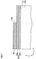
- Step S31 is a step of removing insulating layer 40 formed on first semiconductor layer 20n.
- a resist is applied onto insulating layer 40 by using a photolithography method or a screen printing method.
- the resist is applied onto insulating layer 40 in portions where second semiconductor layer 30p is to be formed.
- portions of insulating layer 40 which are not covered with the resist are dissolved and removed by using an etchant.
- First semiconductor layer 20n is thereby exposed as shown in Fig. 7 .
- second insulating-layer end portion 45b appears.
- First semiconductor layer 20n is also partially removed in some cases depending on processing conditions.
- Examples of methods other than forming a pattern by using a resist include a method of partially removing insulating layer 40 by using an etching paste.
- the methods of partially removing insulating layer 40 are not only limited to these methods and other methods may be used.
- Step S32 is a step of removing first semiconductor layer 20n exposed by the removal of insulating layer 40. Exposed first semiconductor layer 20n is subjected to alkali cleaning. Semiconductor substrate 10n is thereby exposed as shown in Fig. 8 . Moreover, first-semiconductor-layer end portion 27 appears. Amount of first-semiconductor-layer end portion 27 removed changes depending on processing conditions. Hence, when insulating layer 40 is formed to be laid on first semiconductor layer 20n and second semiconductor layer 30p as in solar cell 1A, the processing time is set to be longer for example.
- step S32 insulating layer 40 remaining without being removed serves as a protective film which protects first semiconductor layer 20n. Accordingly, the second insulating-layer end portion and the first-semiconductor-layer end portion are formed to be arranged side by side. Moreover, second insulating-layer end portion 45b and first-semiconductor-layer end portion 27 are at the same position in arrangement direction x.
- Step S33 is a step of forming second semiconductor layer 30p on semiconductor substrate 10n exposed by the removal of first semiconductor layer 20n.
- i-type amorphous semiconductor layer 32i is formed on rear surface 12 of semiconductor substrate 10n.
- p-type amorphous semiconductor layer 35p is formed on thus-formed i-type amorphous semiconductor layer 32i.
- i-type amorphous semiconductor layer 32i and p-type amorphous semiconductor layer 35p are formed by, for example, the CVD method.
- Second semiconductor layer 30p is formed on rear surface 12 in step S33. As shown in Fig. 9 , second semiconductor layer 30p is formed over the entire surface of solar cell 1B. Hence, second semiconductor layer 30p is formed not only on rear surface 12 but also on insulating layer 40.
- second semiconductor layer 30p covers second insulating-layer end portion 45b and first-semiconductor-layer end portion 27.
- Second-semiconductor-layer end portion 37 is an end portion of second semiconductor layer 30p formed on rear surface 12. Hence, first-semiconductor-layer end portion 27 and second-semiconductor-layer end portion 37 are in contact with each other.
- Step S4 is a step of forming first electrode 50n and second electrode 50p.
- Step S4 includes steps S41 to S44.
- Step S41 is a step of removing second semiconductor layer 30p and insulating layer 40.
- a resist is applied onto second semiconductor layer 30p formed on insulating layer 40, in a portion where second semiconductor layer 30p is desired to be left, by using the photolithography method or the screen printing method. Thereafter, processing using an etchant is performed and a portion of second semiconductor layer 30p and a portion of insulating layer 40 on which the resist is applied thereby are left as shown in Fig. 10 .
- a portion of second semiconductor layer 30p and a portion of insulating layer 40 on which no resist is applied are removed. In a case where insulating layer 40 is not completely removed and remains, cleaning is performed by using hydrogen fluoride (HF). First semiconductor layer 20n is thus exposed by this cleaning.
- HF hydrogen fluoride
- Second semiconductor layer 30p and insulating layer 40 may be separately removed. Moreover, as in step S31, second semiconductor layer 30p and insulating layer 40 may be removed by methods other than the method using the resist.
- Step S42 is a step of forming transparent electrode layer 52.
- transparent electrode layer 52 is formed on first semiconductor layer 20n and second semiconductor layer 30p by using a physical vapor deposition method (PVD method).
- PVD method physical vapor deposition method
- an underlying metal layer serving as an underlying layer for collection electrodes 55 may be formed by using the PVD method.
- Ti and Cu are used as underlying metals.
- Step S43 is a step of forming isolation groove 60 for preventing short circuit.
- Isolation groove 60 is formed by using a laser.
- Isolation groove 60 is provided in transparent electrode 52 formed on second semiconductor layer 30p.
- Second semiconductor layer 30p herein is second semiconductor layer 30p formed on insulating layer 40.
- Isolation groove 60 is provided in transparent electrode 52 because first semiconductor layer 20n or second semiconductor layer 30p may otherwise be damaged by the laser. This is similar in the case where isolation groove 60 is formed by methods other than the method using the laser, such as one using a resist and an etchant for example.
- isolation groove 60 is formed in solar cell 1A in such a way that center 60M of isolation groove 60 coincides with center 40M of insulating layer 40 in arrangement direction x.
- isolation groove 60 is formed to be offset to p-type second semiconductor layer 30p in arrangement direction x. Specifically, center 60M of isolation groove 60 is formed closer to center 30pM of second semiconductor layer 30p than center 40M of insulating layer 40 is in arrangement direction x.
- insulating layer 40 can be designed to be smaller in width. This reduces the distance that minor carriers generated under first semiconductor layer 20n move to second semiconductor layer 30p via a portion under insulating layer 40. Accordingly, efficiency deterioration caused by the recombination of minor carries can be suppressed.
- Step S44 is a step of forming collection electrodes 55.
- a conductive paste is applied onto transparent electrode 52 by the screen printing method. Thereafter, collection electrodes 55 are formed by sintering the conductive paste. Collection electrodes 55 may be formed on transparent electrode 52 by plating. Solar cell 1B shown in Fig. 4 is thus formed.
- distance Lp from end point 39 to second insulating-layer end portion 45b in arrangement direction x is shorter than distance Ln from end point 39 to first insulating-layer end portion 45a in arrangement direction x.
- the distance that the minor carriers travel under second semiconductor layer 30p. to reach second electrode 50p is shorter and the recombination of minor carries can be reduced compared to a solar cell in which the width of insulating layer 40 in arrangement direction x is the same.
- the distance Lp from end point 39 to second insulating-layer end portion 45b in arrangement direction x is 0.1 mm or smaller.
- the distance Lp is 0.1 mm or smaller, the number of minor carriers which recombine is small and the conversion efficiency is thereby improved.
- second insulating-layer end portion 45b and first-semiconductor-layer end portion 27 are arranged side by side. Moreover, second insulating-layer end portion 45b and first-semiconductor-layer end portion 27 are at the same position in arrangement direction x.
- the minor carries can move to second electrode 50p without traveling through the portion near the junction between semiconductor substrate 10n and second semiconductor layer 30p covered with insulating layer 40.
- center 60M of isolation groove 60 is closer to center 30pM of second semiconductor layer 30p being the p-type semiconductor than center 40M of insulating layer 40 is. Accordingly, in first semiconductor layer 20n being the n-type semiconductor layer, no damage occurs due to formation of isolation groove 60 even when the width of insulating layer 40 is small. Reducing the width of insulating layer 40 reduces the distance that the minor carriers generated under first semiconductor layer 20n travel to reach second electrode 50p. Accordingly, loss due to recombination of minor carriers can be reduced.
- first semiconductor layer formation step S1, insulating layer formation step S2, and second semiconductor layer formation step S3 are performed in this order.
- Second semiconductor layer formation step S3 includes step S31 of removing insulating layer 40 formed on first semiconductor layer 20n, step S32 of removing first semiconductor layer 20n exposed by the removal of insulating layer 40, and step S33 of forming second semiconductor layer 30p on semiconductor substrate 10n exposed by the removal of first semiconductor layer 20n.
- insulating layer 40 can be used as the protective film for first semiconductor layer 20n.
- the second insulating-layer end portion and the first-semiconductor-layer end portion are formed to be arranged in side by side.
- second insulating-layer end portion 45b and first-semiconductor-layer end portion 27 are formed at the same position in arrangement direction x.
- center 60M of isolation groove 60 is formed to be closer to center 30pM of second semiconductor layer 30p than center 40M of insulating layer 40 is in isolation groove formation step S43. Accordingly, first semiconductor layer 20n being the n-type semiconductor layer is not exposed in the surface and is thereby not damaged by the etchant and the like. Moreover, when isolation groove 60 is formed by using the laser, first semiconductor layer 20n is not damaged by the laser. Accordingly, insulating layer 40 can be designed to be small in width and connection portion between semiconductor substrate 10n and first semiconductor layer 20n under insulating layer 40 can be made smaller. Hence, the distance that the minor carriers travel under first semiconductor layer 20n can be made shorter.
- the conductivity type of semiconductor substrate 10n is n-type.
- the invention is not limited to this.
- p-type semiconductor substrate 10p may be used.
- the minor carriers are electrons. Accordingly, in solar cell 1C, distance Lp from end point 39 to first insulating layer end portion 45a in arrangement direction x is longer than distance Ln from end point 39 to second insulating layer end portion 45b in arrangement direction x.
- second insulating-layer end portion 45b and first-semiconductor-layer end portion 27 are arranged side by side. Second insulating-layer end portion 45b and first-semiconductor-layer end portion 27 are at the same position in arrangement direction x.
- center 60M of isolation groove 60 is closer to center 20pM of the first semiconductor layer being the p-type semiconductor layer in arrangement direction x than center 40M of insulating layer 40 is in arrangement direction x.
- isolation groove 60 is provided in transparent electrode 52 formed on second semiconductor layer 30p formed on insulating layer 40.
- part of isolation groove 60 may be provided in transparent electrode 52 formed on second semiconductor layer 30p formed on rear surface 12 due to misalignment.
- the thickness of second semiconductor layer 30p covering second insulating-layer end portion 45b and first-semiconductor-layer end portion 27 is small, there is a possibility of short circuit occurring since the distance between transparent electrode layer 52p and first semiconductor layer 20n is close. Forming isolation groove 65 being part of isolation groove 60 reduces the possibility of such short circuit occurring.
- the isolation groove 65 may be provided in transparent electrode 52 formed on second semiconductor layer 30p formed on rear surface 12 to prevent short circuit.
- the invention includes various embodiments which are not described herein. Accordingly, the technical scope of the invention should be determined only by the matters to define the invention in the scope of claims regarded as appropriate based on the above description.
Landscapes
- Photovoltaic Devices (AREA)
- Life Sciences & Earth Sciences (AREA)
- Engineering & Computer Science (AREA)
- Sustainable Energy (AREA)
- Sustainable Development (AREA)
Claims (13)
- Solarzelle, die Folgendes umfasst:ein Halbleitersubstrat (10n) eines ersten Leitfähigkeitstyps mit einer lichtempfangenden Seite und einer Rückseite (12);eine erste Halbleiterschicht (20n) des ersten Leitfähigkeitstyps;eine zweite Halbleiterschicht (30p) eines zweiten Leitfähigkeitstyps;eine erste Elektrode (50n), die mit der ersten Halbleiterschicht (20n) elektrisch verbunden ist;eine zweite Elektrode (50p), die mit der zweiten Halbleiterschicht (30p) elektrisch verbunden ist; undeine Isolationsschicht (40) mit isolierenden Eigenschaften,worin die erste Halbleiterschicht (20n) und die zweite Halbleiterschicht (30p) auf der Rückseite (12) ausgebildet sind und die erste Halbleiterschicht (20n) und die zweite Halbleiterschicht (30p) einander auf der Rückseite (12) an deren Grenzfläche berühren, so dass die Isolationsschicht (40) auf der Grenzfläche zwischen der ersten Halbleiterschicht (20n) und der zweiten Halbleiterschicht (30p) und sowohl auf der ersten Halbleiterschicht (20n) als auch auf der zweiten Halbleiterschicht (30p) ausgebildet ist,wenn ein Endabschnitt der ersten Halbleiterschicht (20n) als erster Halbleiterschicht-Endabschnitt (27) definiert ist, ein Endabschnitt der zweiten Halbleiterschicht (30p), der den Endabschnitt der ersten Halbleiterschicht (20n) berührt, als ein zweiter Halbleiterschicht-Endabschnitt (37) definiert ist, ein Endabschnitt der Isolationsschicht (40), der auf der ersten Halbleiterschicht (20n) ausgebildet ist und auf der Seite der ersten Elektrode (50n) vorliegt, als erster Isolationsschicht-Endabschnitt (45a) definiert ist und ein weiterer Endabschnitt der Isolationsschicht (40), der auf der Seite der zweiten Elektrode (50p) vorliegt, als ein zweiter Isolationsschicht-Endabschnitt (45b) definiert ist, in einer Anordnungsrichtung, in der die erste Halbleiterschicht (20n) und die zweite Halbleiterschicht (30p) abwechselnd angeordnet sind, dadurch gekennzeichnet, dassein Abstand von einem Endpunkt (39) des zweiten Halbleiterschicht-Endabschnitts (37) in Kontakt mit der Rückseite (12) zu dem zweiten Isolationsschicht-Endabschnitt (45b) in der Anordnungsrichtung geringer ist als ein Abstand von dem Endpunkt (39) zu dem ersten Isolationsschicht-Endabschnitt (45a) in der Anordnungsrichtung.
- Solarzelle nach Anspruch 1, worin der Abstand von dem Endpunkt (39) zu dem zweiten Isolationsschicht-Endabschnitt (37) in Anordnungsrichtung 0,1 mm beträgt oder geringer ist.
- Solarzelle nach Anspruch 1, die ferner eine Isolationsnut (60) umfasst, um einen Kurzschluss zu verhindern, wobei die Isolationsnut (60) auf der Isolationsschicht (40) angeordnet ist.
- Solarzelle nach Anspruch 3, worin eine der ersten oder der zweiten Halbleiterschicht (20n, 30p) eine Leitfähigkeit vom p-Typ aufweist und ein Mittelpunkt der Isolationsnut (60) näher an einem Mittelpunkt der p-Typ-Halbleiterschicht vorliegt als zu einem Mittelpunkt der Isolationsschicht (40) in der Anordnungsrichtung.
- Solarzelle nach Anspruch 1, worin eine vollständige lichtempfangende Oberfläche in der Lage ist, Licht zu empfangen und mit einer Passivierungsschicht bedeckt ist, die eine im Wesentlichen intrinsisch amorphe Halbleiterschicht umfasst.
- Verfahren zur Herstellung einer Solarzelle, das Folgendes umfasst:einen ersten Halbleiterschichtausbildungsschritt zur Ausbildung einer ersten Halbleiterschicht (20n) eines ersten Leitfähigkeitstyps auf einer Rückseite (12) eines Halbleitersubstrats (10n) des ersten Leitfähigkeitstyps, wobei das Halbleitersubstrat (10n) eine lichtempfangende Oberfläche aufweist, die ausgebildet ist, um Licht zu empfangen, und die Rückseite (12) auf einer der lichtempfangenden Seite entgegengesetzten Seite ausgebildet ist;einen zweiten Halbleiterschichtausbildungsschritt zur Ausbildung einer zweiten Halbleiterschicht (30p) eines zweiten Leitfähigkeitstyps auf der Rückseite (12);einen Isolationsschichtausbildungsschritt zur Ausbildung einer Isolationsschicht (40) mit isolierenden Eigenschaften, wobei die erste Halbleiterschicht (20n) und die zweite Halbleiterschicht (30p) einander auf der Rückseite (12) an deren Grenzfläche berühren, so dass die Isolationsschicht (40) auf der Grenzfläche zwischen der ersten Halbleiterschicht (20n) und der zweiten Halbleiterschicht (30p) und sowohl auf der ersten Halbleiterschicht (20n) als auch auf der zweiten Halbleiterschicht (30p) ausgebildet wird; dadurch gekennzeichnet, dass:die Schritte in folgender Reihenfolge durchgeführt werden: erster Halbleiterschicht- (20n) Ausbildungsschritt, Isolationsschicht- (40) Ausbildungsschritt, zweiter Halbleiterschicht- (30p) Ausbildungsschritt,wobei der zweite Halbleiterschichtausbildungsschritt folgende Schritte umfasst:das Entfernen eines Teils der Isolationsschicht (40), die auf der ersten Halbleiterschicht (20n) ausgebildet ist;das Entfernen der durch das Entfernen der Isolationsschicht (40) freigesetzten ersten Halbleiterschicht (40) unddas Ausbilden der zweiten Halbleiterschicht (30p) auf dem durch das Entfernen der ersten Halbleiterschicht (20n) freigelegten Halbleitersubstrat (10n).
- Verfahren zur Herstellung einer Solarzelle nach Anspruch 6, worin der erste Halbleiterschicht- (20n) Ausbildungsschritt einen Schritt des Ausbildens der ersten Halbleiterschicht (20n) auf fast der gesamten Rückseite des Halbleitersubstrats (12) umfasst.
- Verfahren zur Herstellung einer Solarzelle nach Anspruch 7, worin der Isolationsschicht- (40) Ausbildungsschritt einen Schritt des Ausbildens der Isolationsschicht (40) fast auf der gesamten Oberfläche der ersten Halbleiterschicht (20n) umfasst.
- Verfahren zur Herstellung einer Solarzelle nach Anspruch 6, das ferner einen Isolationsnut- (60) Ausbildungsschritt zur Ausbildung einer Isolationsnut (60) zur Verhinderung von Kurzschlüssen umfasst, wobei in dem Isolationsnutausbildungsschritt die Isolationsnut (60) auf der Isolationsschicht (40) ausgebildet wird.
- Verfahren zur Herstellung einer Solarzelle nach Anspruch 9, worin eine der ersten oder zweiten Halbleiterschicht (20n, 30p) eine Leitfähigkeit vom p-Typ aufweist und in dem Isolationsnutausbildungsschritt ein Mittelpunkt der Isolationsnut (60) näher an einem Mittelpunkt der p-Typ-Halbleiterschicht ausgebildet wird als zu einem Mittelpunkt der Isolationsschicht (40) in einer Anordnungsrichtung, in der die erste Halbleiterschicht (20n) und die zweite Halbleiterschicht (30p) abwechselnd angeordnet sind.
- Verfahren zur Herstellung einer Solarzelle nach Anspruch 9, worin die Isolationsnut (60) einen Kurzschluss zwischen einer ersten Elektrode (50n), die mit der ersten Halbleiterschicht (20n) verbunden ist, und einer zweiten Elektrode (50p), die mit der zweiten Halbleiterschicht (30p) verbunden ist, verhindert.
- Verfahren zur Herstellung einer Solarzelle nach Anspruch 6, das ferner einen Elektrodenausbildungsschritt zur Ausbildung einer ersten Elektrode (50n), die mit der ersten Halbleiterschicht (20n) verbunden ist, und einer zweiten Elektrode (50p), die mit der zweiten Halbleiterschicht (30p) verbunden ist, umfasst, wobei der Elektrodenausbildungsschritt folgende Schritte umfasst:das Ausbilden einer Elektrodenschicht durchgehend auf einer Oberfläche der ersten Halbleiterschicht (20n) und einer Oberfläche der zweiten Halbleiterschicht (30p) unddas Ausbilden einer Isolationsnut (60) in der Elektrodenschicht auf der Isolationsschicht (40).
- Verfahren zur Herstellung einer Solarzelle nach Anspruch 12, worin der Elektrodenausbildungsschritt folgende Schritte umfasst:das Ausbilden einer transparenten Elektrodenschicht unddas Ausbilden einer Sammelelektrode,wobei der Schritt des Ausbildens einer transparenten Elektrodenschicht einen Schritt des Ausbildens eines transparenten Elektrodenfilms durchgehend auf einer Oberfläche der ersten Halbleiterschicht (20n) und auf einer Oberfläche der zweiten Halbleiterschicht (30p) und das Ausbilden der Isolationsnut (60) in dem transparenten Elektrodenfilm auf der Isolationsschicht (40) umfasst, undwobei der Schritt des Ausbildens einer Sammelelektrode einen Schritt des Ausbildens der Sammelelektrode auf allen Abschnitten der transparenten Elektrodenschicht umfasst, die durch die Isolationsnut (60) isoliert ist.
Applications Claiming Priority (2)
| Application Number | Priority Date | Filing Date | Title |
|---|---|---|---|
| JP2010042330 | 2010-02-26 | ||
| PCT/JP2011/054310 WO2011105554A1 (ja) | 2010-02-26 | 2011-02-25 | 太陽電池及び太陽電池の製造方法 |
Publications (3)
| Publication Number | Publication Date |
|---|---|
| EP2541617A1 EP2541617A1 (de) | 2013-01-02 |
| EP2541617A4 EP2541617A4 (de) | 2013-12-18 |
| EP2541617B1 true EP2541617B1 (de) | 2017-03-22 |
Family
ID=44506951
Family Applications (1)
| Application Number | Title | Priority Date | Filing Date |
|---|---|---|---|
| EP11747510.3A Not-in-force EP2541617B1 (de) | 2010-02-26 | 2011-02-25 | Solarzelle und verfahren zur herstellung einer solarzelle |
Country Status (5)
| Country | Link |
|---|---|
| US (1) | US9252301B2 (de) |
| EP (1) | EP2541617B1 (de) |
| JP (1) | JP5906393B2 (de) |
| TW (1) | TW201143113A (de) |
| WO (1) | WO2011105554A1 (de) |
Families Citing this family (24)
| Publication number | Priority date | Publication date | Assignee | Title |
|---|---|---|---|---|
| JP5956742B2 (ja) * | 2011-11-14 | 2016-07-27 | シャープ株式会社 | 光電変換素子 |
| US8597970B2 (en) | 2011-12-21 | 2013-12-03 | Sunpower Corporation | Hybrid polysilicon heterojunction back contact cell |
| JP5820265B2 (ja) * | 2011-12-21 | 2015-11-24 | シャープ株式会社 | 裏面電極型太陽電池及びその製造方法 |
| FR2985608B1 (fr) * | 2012-01-05 | 2016-11-18 | Commissariat Energie Atomique | Cellule photovoltaique et procede de realisation |
| GB2503515A (en) * | 2012-06-29 | 2014-01-01 | Rec Cells Pte Ltd | A rear contact heterojunction solar cell |
| KR101977927B1 (ko) * | 2012-07-11 | 2019-05-13 | 인텔렉츄얼 키스톤 테크놀로지 엘엘씨 | 광전소자 및 그 제조방법 |
| US9312406B2 (en) | 2012-12-19 | 2016-04-12 | Sunpower Corporation | Hybrid emitter all back contact solar cell |
| US9640699B2 (en) * | 2013-02-08 | 2017-05-02 | International Business Machines Corporation | Interdigitated back contact heterojunction photovoltaic device |
| US9859455B2 (en) | 2013-02-08 | 2018-01-02 | International Business Machines Corporation | Interdigitated back contact heterojunction photovoltaic device with a floating junction front surface field |
| JP6360471B2 (ja) * | 2013-03-04 | 2018-07-18 | シャープ株式会社 | 光電変換素子、光電変換モジュールおよび太陽光発電システム |
| WO2014157525A1 (ja) * | 2013-03-28 | 2014-10-02 | シャープ株式会社 | 光電変換素子 |
| US9761743B2 (en) | 2013-03-28 | 2017-09-12 | Sharp Kabushiki Kaisha | Photoelectric conversion element |
| US9196758B2 (en) | 2013-12-20 | 2015-11-24 | Sunpower Corporation | Solar cell emitter region fabrication with differentiated p-type and n-type region architectures |
| JP6425143B2 (ja) * | 2014-01-28 | 2018-11-21 | パナソニックIpマネジメント株式会社 | 太陽電池及びその製造方法 |
| JP2015185743A (ja) * | 2014-03-25 | 2015-10-22 | シャープ株式会社 | 光電変換素子 |
| US9837576B2 (en) | 2014-09-19 | 2017-12-05 | Sunpower Corporation | Solar cell emitter region fabrication with differentiated P-type and N-type architectures and incorporating dotted diffusion |
| JP2016143862A (ja) * | 2015-02-05 | 2016-08-08 | シャープ株式会社 | 光電変換素子および光電変換素子の製造方法 |
| US9525083B2 (en) | 2015-03-27 | 2016-12-20 | Sunpower Corporation | Solar cell emitter region fabrication with differentiated P-type and N-type architectures and incorporating a multi-purpose passivation and contact layer |
| US11355657B2 (en) * | 2015-03-27 | 2022-06-07 | Sunpower Corporation | Metallization of solar cells with differentiated p-type and n-type region architectures |
| JP6712605B2 (ja) * | 2015-12-07 | 2020-06-24 | 株式会社カネカ | 光電変換装置およびその製造方法 |
| JP6788874B2 (ja) * | 2016-03-28 | 2020-11-25 | パナソニックIpマネジメント株式会社 | 太陽電池セル及びその製造方法 |
| US9502601B1 (en) | 2016-04-01 | 2016-11-22 | Sunpower Corporation | Metallization of solar cells with differentiated P-type and N-type region architectures |
| FR3073670B1 (fr) * | 2017-11-15 | 2019-12-13 | Commissariat A L'energie Atomique Et Aux Energies Alternatives | Procede de formation d'electrodes |
| CN117690983A (zh) | 2023-12-28 | 2024-03-12 | 浙江晶科能源有限公司 | 太阳能电池及光伏组件 |
Family Cites Families (9)
| Publication number | Priority date | Publication date | Assignee | Title |
|---|---|---|---|---|
| JP2004193350A (ja) * | 2002-12-11 | 2004-07-08 | Sharp Corp | 太陽電池セルおよびその製造方法 |
| US7388147B2 (en) * | 2003-04-10 | 2008-06-17 | Sunpower Corporation | Metal contact structure for solar cell and method of manufacture |
| US7339110B1 (en) * | 2003-04-10 | 2008-03-04 | Sunpower Corporation | Solar cell and method of manufacture |
| FR2880989B1 (fr) * | 2005-01-20 | 2007-03-09 | Commissariat Energie Atomique | Dispositif semi-conducteur a heterojonctions et a structure inter-digitee |
| DE102008030880A1 (de) * | 2007-12-11 | 2009-06-18 | Institut Für Solarenergieforschung Gmbh | Rückkontaktsolarzelle mit großflächigen Rückseiten-Emitterbereichen und Herstellungsverfahren hierfür |
| US20110000532A1 (en) * | 2008-01-30 | 2011-01-06 | Kyocera Corporation | Solar Cell Device and Method of Manufacturing Solar Cell Device |
| JP5230222B2 (ja) * | 2008-02-21 | 2013-07-10 | 三洋電機株式会社 | 太陽電池 |
| US7999175B2 (en) * | 2008-09-09 | 2011-08-16 | Palo Alto Research Center Incorporated | Interdigitated back contact silicon solar cells with laser ablated grooves |
| US8258050B2 (en) * | 2009-07-17 | 2012-09-04 | Hewlett-Packard Development Company, L.P. | Method of making light trapping crystalline structures |
-
2011
- 2011-02-25 EP EP11747510.3A patent/EP2541617B1/de not_active Not-in-force
- 2011-02-25 JP JP2012501883A patent/JP5906393B2/ja not_active Expired - Fee Related
- 2011-02-25 TW TW100106348A patent/TW201143113A/zh unknown
- 2011-02-25 WO PCT/JP2011/054310 patent/WO2011105554A1/ja not_active Ceased
-
2012
- 2012-08-24 US US13/594,201 patent/US9252301B2/en not_active Expired - Fee Related
Non-Patent Citations (1)
| Title |
|---|
| None * |
Also Published As
| Publication number | Publication date |
|---|---|
| WO2011105554A1 (ja) | 2011-09-01 |
| JPWO2011105554A1 (ja) | 2013-06-20 |
| US9252301B2 (en) | 2016-02-02 |
| EP2541617A1 (de) | 2013-01-02 |
| TW201143113A (en) | 2011-12-01 |
| US20130247970A1 (en) | 2013-09-26 |
| JP5906393B2 (ja) | 2016-04-20 |
| EP2541617A4 (de) | 2013-12-18 |
Similar Documents
| Publication | Publication Date | Title |
|---|---|---|
| EP2541617B1 (de) | Solarzelle und verfahren zur herstellung einer solarzelle | |
| EP2530729B1 (de) | Solarzelle und herstellungsverfahren dafür | |
| US10727360B2 (en) | Photoelectric conversion device and method for manufacturing same | |
| US9006564B2 (en) | Method of manufacturing solar cell and solar cell | |
| US9142706B2 (en) | Method of manufacturing solar cell | |
| US9508888B2 (en) | Solar cell with silicon nitride layer and method for manufacturing same | |
| US8664034B2 (en) | Method of manufacturing solar cell | |
| US8877545B2 (en) | Method of manufacturing solar cell | |
| US20120090674A1 (en) | Solar cell | |
| US9530913B2 (en) | Solar cell | |
| US9780241B2 (en) | Solar cell | |
| US9627557B2 (en) | Solar cell | |
| US12107176B2 (en) | Solar cell and method for manufacturing solar cell | |
| US10014420B2 (en) | Solar cell | |
| US20140020741A1 (en) | Solar cell and method for producing solar cell | |
| JP6425143B2 (ja) | 太陽電池及びその製造方法 | |
| US20140020755A1 (en) | Solar cell and method for producing solar cell |
Legal Events
| Date | Code | Title | Description |
|---|---|---|---|
| PUAI | Public reference made under article 153(3) epc to a published international application that has entered the european phase |
Free format text: ORIGINAL CODE: 0009012 |
|
| 17P | Request for examination filed |
Effective date: 20120921 |
|
| AK | Designated contracting states |
Kind code of ref document: A1 Designated state(s): AL AT BE BG CH CY CZ DE DK EE ES FI FR GB GR HR HU IE IS IT LI LT LU LV MC MK MT NL NO PL PT RO RS SE SI SK SM TR |
|
| DAX | Request for extension of the european patent (deleted) | ||
| A4 | Supplementary search report drawn up and despatched |
Effective date: 20131120 |
|
| RIC1 | Information provided on ipc code assigned before grant |
Ipc: H01L 31/04 20060101AFI20131114BHEP Ipc: H01L 31/18 20060101ALI20131114BHEP Ipc: H01L 31/0747 20120101ALI20131114BHEP Ipc: H01L 31/068 20120101ALI20131114BHEP Ipc: H01L 31/0224 20060101ALI20131114BHEP |
|
| 17Q | First examination report despatched |
Effective date: 20150603 |
|
| RAP1 | Party data changed (applicant data changed or rights of an application transferred) |
Owner name: PANASONIC INTELLECTUAL PROPERTY MANAGEMENT CO., LT |
|
| GRAP | Despatch of communication of intention to grant a patent |
Free format text: ORIGINAL CODE: EPIDOSNIGR1 |
|
| INTG | Intention to grant announced |
Effective date: 20161107 |
|
| RIN1 | Information on inventor provided before grant (corrected) |
Inventor name: IDE DAISUKE Inventor name: MORIGAMI MITSUAKI Inventor name: SAKATA HITOSHI Inventor name: SHIGEMATSU MASATO Inventor name: HISHIDA YUJI Inventor name: MORI HIROYUKI Inventor name: MISHIMA TAKAHIRO |
|
| GRAS | Grant fee paid |
Free format text: ORIGINAL CODE: EPIDOSNIGR3 |
|
| GRAA | (expected) grant |
Free format text: ORIGINAL CODE: 0009210 |
|
| AK | Designated contracting states |
Kind code of ref document: B1 Designated state(s): AL AT BE BG CH CY CZ DE DK EE ES FI FR GB GR HR HU IE IS IT LI LT LU LV MC MK MT NL NO PL PT RO RS SE SI SK SM TR |
|
| REG | Reference to a national code |
Ref country code: GB Ref legal event code: FG4D |
|
| REG | Reference to a national code |
Ref country code: CH Ref legal event code: EP |
|
| REG | Reference to a national code |
Ref country code: AT Ref legal event code: REF Ref document number: 878544 Country of ref document: AT Kind code of ref document: T Effective date: 20170415 |
|
| REG | Reference to a national code |
Ref country code: IE Ref legal event code: FG4D |
|
| REG | Reference to a national code |
Ref country code: DE Ref legal event code: R096 Ref document number: 602011036232 Country of ref document: DE |
|
| REG | Reference to a national code |
Ref country code: NL Ref legal event code: MP Effective date: 20170322 |
|
| PG25 | Lapsed in a contracting state [announced via postgrant information from national office to epo] |
Ref country code: HR Free format text: LAPSE BECAUSE OF FAILURE TO SUBMIT A TRANSLATION OF THE DESCRIPTION OR TO PAY THE FEE WITHIN THE PRESCRIBED TIME-LIMIT Effective date: 20170322 Ref country code: NO Free format text: LAPSE BECAUSE OF FAILURE TO SUBMIT A TRANSLATION OF THE DESCRIPTION OR TO PAY THE FEE WITHIN THE PRESCRIBED TIME-LIMIT Effective date: 20170622 Ref country code: GR Free format text: LAPSE BECAUSE OF FAILURE TO SUBMIT A TRANSLATION OF THE DESCRIPTION OR TO PAY THE FEE WITHIN THE PRESCRIBED TIME-LIMIT Effective date: 20170623 Ref country code: FI Free format text: LAPSE BECAUSE OF FAILURE TO SUBMIT A TRANSLATION OF THE DESCRIPTION OR TO PAY THE FEE WITHIN THE PRESCRIBED TIME-LIMIT Effective date: 20170322 Ref country code: LT Free format text: LAPSE BECAUSE OF FAILURE TO SUBMIT A TRANSLATION OF THE DESCRIPTION OR TO PAY THE FEE WITHIN THE PRESCRIBED TIME-LIMIT Effective date: 20170322 |
|
| REG | Reference to a national code |
Ref country code: LT Ref legal event code: MG4D |
|
| REG | Reference to a national code |
Ref country code: AT Ref legal event code: MK05 Ref document number: 878544 Country of ref document: AT Kind code of ref document: T Effective date: 20170322 |
|
| PG25 | Lapsed in a contracting state [announced via postgrant information from national office to epo] |
Ref country code: RS Free format text: LAPSE BECAUSE OF FAILURE TO SUBMIT A TRANSLATION OF THE DESCRIPTION OR TO PAY THE FEE WITHIN THE PRESCRIBED TIME-LIMIT Effective date: 20170322 Ref country code: LV Free format text: LAPSE BECAUSE OF FAILURE TO SUBMIT A TRANSLATION OF THE DESCRIPTION OR TO PAY THE FEE WITHIN THE PRESCRIBED TIME-LIMIT Effective date: 20170322 Ref country code: BG Free format text: LAPSE BECAUSE OF FAILURE TO SUBMIT A TRANSLATION OF THE DESCRIPTION OR TO PAY THE FEE WITHIN THE PRESCRIBED TIME-LIMIT Effective date: 20170622 Ref country code: SE Free format text: LAPSE BECAUSE OF FAILURE TO SUBMIT A TRANSLATION OF THE DESCRIPTION OR TO PAY THE FEE WITHIN THE PRESCRIBED TIME-LIMIT Effective date: 20170322 |
|
| PG25 | Lapsed in a contracting state [announced via postgrant information from national office to epo] |
Ref country code: NL Free format text: LAPSE BECAUSE OF FAILURE TO SUBMIT A TRANSLATION OF THE DESCRIPTION OR TO PAY THE FEE WITHIN THE PRESCRIBED TIME-LIMIT Effective date: 20170322 |
|
| PG25 | Lapsed in a contracting state [announced via postgrant information from national office to epo] |
Ref country code: SK Free format text: LAPSE BECAUSE OF FAILURE TO SUBMIT A TRANSLATION OF THE DESCRIPTION OR TO PAY THE FEE WITHIN THE PRESCRIBED TIME-LIMIT Effective date: 20170322 Ref country code: EE Free format text: LAPSE BECAUSE OF FAILURE TO SUBMIT A TRANSLATION OF THE DESCRIPTION OR TO PAY THE FEE WITHIN THE PRESCRIBED TIME-LIMIT Effective date: 20170322 Ref country code: RO Free format text: LAPSE BECAUSE OF FAILURE TO SUBMIT A TRANSLATION OF THE DESCRIPTION OR TO PAY THE FEE WITHIN THE PRESCRIBED TIME-LIMIT Effective date: 20170322 Ref country code: CZ Free format text: LAPSE BECAUSE OF FAILURE TO SUBMIT A TRANSLATION OF THE DESCRIPTION OR TO PAY THE FEE WITHIN THE PRESCRIBED TIME-LIMIT Effective date: 20170322 Ref country code: AT Free format text: LAPSE BECAUSE OF FAILURE TO SUBMIT A TRANSLATION OF THE DESCRIPTION OR TO PAY THE FEE WITHIN THE PRESCRIBED TIME-LIMIT Effective date: 20170322 Ref country code: ES Free format text: LAPSE BECAUSE OF FAILURE TO SUBMIT A TRANSLATION OF THE DESCRIPTION OR TO PAY THE FEE WITHIN THE PRESCRIBED TIME-LIMIT Effective date: 20170322 |
|
| PG25 | Lapsed in a contracting state [announced via postgrant information from national office to epo] |
Ref country code: IS Free format text: LAPSE BECAUSE OF FAILURE TO SUBMIT A TRANSLATION OF THE DESCRIPTION OR TO PAY THE FEE WITHIN THE PRESCRIBED TIME-LIMIT Effective date: 20170722 Ref country code: PL Free format text: LAPSE BECAUSE OF FAILURE TO SUBMIT A TRANSLATION OF THE DESCRIPTION OR TO PAY THE FEE WITHIN THE PRESCRIBED TIME-LIMIT Effective date: 20170322 Ref country code: SM Free format text: LAPSE BECAUSE OF FAILURE TO SUBMIT A TRANSLATION OF THE DESCRIPTION OR TO PAY THE FEE WITHIN THE PRESCRIBED TIME-LIMIT Effective date: 20170322 Ref country code: PT Free format text: LAPSE BECAUSE OF FAILURE TO SUBMIT A TRANSLATION OF THE DESCRIPTION OR TO PAY THE FEE WITHIN THE PRESCRIBED TIME-LIMIT Effective date: 20170724 |
|
| REG | Reference to a national code |
Ref country code: DE Ref legal event code: R097 Ref document number: 602011036232 Country of ref document: DE |
|
| PLBE | No opposition filed within time limit |
Free format text: ORIGINAL CODE: 0009261 |
|
| STAA | Information on the status of an ep patent application or granted ep patent |
Free format text: STATUS: NO OPPOSITION FILED WITHIN TIME LIMIT |
|
| PG25 | Lapsed in a contracting state [announced via postgrant information from national office to epo] |
Ref country code: DK Free format text: LAPSE BECAUSE OF FAILURE TO SUBMIT A TRANSLATION OF THE DESCRIPTION OR TO PAY THE FEE WITHIN THE PRESCRIBED TIME-LIMIT Effective date: 20170322 |
|
| REG | Reference to a national code |
Ref country code: FR Ref legal event code: PLFP Year of fee payment: 8 |
|
| 26N | No opposition filed |
Effective date: 20180102 |
|
| PG25 | Lapsed in a contracting state [announced via postgrant information from national office to epo] |
Ref country code: SI Free format text: LAPSE BECAUSE OF FAILURE TO SUBMIT A TRANSLATION OF THE DESCRIPTION OR TO PAY THE FEE WITHIN THE PRESCRIBED TIME-LIMIT Effective date: 20170322 Ref country code: IT Free format text: LAPSE BECAUSE OF FAILURE TO SUBMIT A TRANSLATION OF THE DESCRIPTION OR TO PAY THE FEE WITHIN THE PRESCRIBED TIME-LIMIT Effective date: 20170322 |
|
| REG | Reference to a national code |
Ref country code: CH Ref legal event code: PL |
|
| PG25 | Lapsed in a contracting state [announced via postgrant information from national office to epo] |
Ref country code: MC Free format text: LAPSE BECAUSE OF FAILURE TO SUBMIT A TRANSLATION OF THE DESCRIPTION OR TO PAY THE FEE WITHIN THE PRESCRIBED TIME-LIMIT Effective date: 20170322 |
|
| GBPC | Gb: european patent ceased through non-payment of renewal fee |
Effective date: 20180225 |
|
| REG | Reference to a national code |
Ref country code: IE Ref legal event code: MM4A |
|
| REG | Reference to a national code |
Ref country code: BE Ref legal event code: MM Effective date: 20180228 |
|
| PG25 | Lapsed in a contracting state [announced via postgrant information from national office to epo] |
Ref country code: CH Free format text: LAPSE BECAUSE OF NON-PAYMENT OF DUE FEES Effective date: 20180228 Ref country code: LU Free format text: LAPSE BECAUSE OF NON-PAYMENT OF DUE FEES Effective date: 20180225 Ref country code: LI Free format text: LAPSE BECAUSE OF NON-PAYMENT OF DUE FEES Effective date: 20180228 |
|
| PG25 | Lapsed in a contracting state [announced via postgrant information from national office to epo] |
Ref country code: IE Free format text: LAPSE BECAUSE OF NON-PAYMENT OF DUE FEES Effective date: 20180225 |
|
| PG25 | Lapsed in a contracting state [announced via postgrant information from national office to epo] |
Ref country code: BE Free format text: LAPSE BECAUSE OF NON-PAYMENT OF DUE FEES Effective date: 20180228 Ref country code: GB Free format text: LAPSE BECAUSE OF NON-PAYMENT OF DUE FEES Effective date: 20180225 |
|
| PG25 | Lapsed in a contracting state [announced via postgrant information from national office to epo] |
Ref country code: MT Free format text: LAPSE BECAUSE OF NON-PAYMENT OF DUE FEES Effective date: 20180225 |
|
| PG25 | Lapsed in a contracting state [announced via postgrant information from national office to epo] |
Ref country code: TR Free format text: LAPSE BECAUSE OF FAILURE TO SUBMIT A TRANSLATION OF THE DESCRIPTION OR TO PAY THE FEE WITHIN THE PRESCRIBED TIME-LIMIT Effective date: 20170322 |
|
| PG25 | Lapsed in a contracting state [announced via postgrant information from national office to epo] |
Ref country code: HU Free format text: LAPSE BECAUSE OF FAILURE TO SUBMIT A TRANSLATION OF THE DESCRIPTION OR TO PAY THE FEE WITHIN THE PRESCRIBED TIME-LIMIT; INVALID AB INITIO Effective date: 20110225 |
|
| PG25 | Lapsed in a contracting state [announced via postgrant information from national office to epo] |
Ref country code: CY Free format text: LAPSE BECAUSE OF FAILURE TO SUBMIT A TRANSLATION OF THE DESCRIPTION OR TO PAY THE FEE WITHIN THE PRESCRIBED TIME-LIMIT Effective date: 20170322 Ref country code: MK Free format text: LAPSE BECAUSE OF NON-PAYMENT OF DUE FEES Effective date: 20170322 |
|
| PG25 | Lapsed in a contracting state [announced via postgrant information from national office to epo] |
Ref country code: AL Free format text: LAPSE BECAUSE OF FAILURE TO SUBMIT A TRANSLATION OF THE DESCRIPTION OR TO PAY THE FEE WITHIN THE PRESCRIBED TIME-LIMIT Effective date: 20170322 |
|
| PGFP | Annual fee paid to national office [announced via postgrant information from national office to epo] |
Ref country code: FR Payment date: 20210225 Year of fee payment: 11 |
|
| PGFP | Annual fee paid to national office [announced via postgrant information from national office to epo] |
Ref country code: DE Payment date: 20210217 Year of fee payment: 11 |
|
| REG | Reference to a national code |
Ref country code: DE Ref legal event code: R119 Ref document number: 602011036232 Country of ref document: DE |
|
| PG25 | Lapsed in a contracting state [announced via postgrant information from national office to epo] |
Ref country code: FR Free format text: LAPSE BECAUSE OF NON-PAYMENT OF DUE FEES Effective date: 20220228 |
|
| PG25 | Lapsed in a contracting state [announced via postgrant information from national office to epo] |
Ref country code: DE Free format text: LAPSE BECAUSE OF NON-PAYMENT OF DUE FEES Effective date: 20220901 |