EP2410568A2 - Cellule solaire et son procédé de fabrication - Google Patents
Cellule solaire et son procédé de fabrication Download PDFInfo
- Publication number
- EP2410568A2 EP2410568A2 EP11154459A EP11154459A EP2410568A2 EP 2410568 A2 EP2410568 A2 EP 2410568A2 EP 11154459 A EP11154459 A EP 11154459A EP 11154459 A EP11154459 A EP 11154459A EP 2410568 A2 EP2410568 A2 EP 2410568A2
- Authority
- EP
- European Patent Office
- Prior art keywords
- doping region
- doping
- layer
- substrate
- solar cell
- Prior art date
- Legal status (The legal status is an assumption and is not a legal conclusion. Google has not performed a legal analysis and makes no representation as to the accuracy of the status listed.)
- Withdrawn
Links
Images


Classifications
-
- H—ELECTRICITY
- H10—SEMICONDUCTOR DEVICES; ELECTRIC SOLID-STATE DEVICES NOT OTHERWISE PROVIDED FOR
- H10F—INORGANIC SEMICONDUCTOR DEVICES SENSITIVE TO INFRARED RADIATION, LIGHT, ELECTROMAGNETIC RADIATION OF SHORTER WAVELENGTH OR CORPUSCULAR RADIATION
- H10F77/00—Constructional details of devices covered by this subclass
- H10F77/10—Semiconductor bodies
- H10F77/14—Shape of semiconductor bodies; Shapes, relative sizes or dispositions of semiconductor regions within semiconductor bodies
-
- H—ELECTRICITY
- H10—SEMICONDUCTOR DEVICES; ELECTRIC SOLID-STATE DEVICES NOT OTHERWISE PROVIDED FOR
- H10F—INORGANIC SEMICONDUCTOR DEVICES SENSITIVE TO INFRARED RADIATION, LIGHT, ELECTROMAGNETIC RADIATION OF SHORTER WAVELENGTH OR CORPUSCULAR RADIATION
- H10F19/00—Integrated devices, or assemblies of multiple devices, comprising at least one photovoltaic cell covered by group H10F10/00, e.g. photovoltaic modules
- H10F19/20—Integrated devices, or assemblies of multiple devices, comprising at least one photovoltaic cell covered by group H10F10/00, e.g. photovoltaic modules comprising photovoltaic cells in arrays in or on a single semiconductor substrate, the photovoltaic cells having planar junctions
-
- H—ELECTRICITY
- H10—SEMICONDUCTOR DEVICES; ELECTRIC SOLID-STATE DEVICES NOT OTHERWISE PROVIDED FOR
- H10F—INORGANIC SEMICONDUCTOR DEVICES SENSITIVE TO INFRARED RADIATION, LIGHT, ELECTROMAGNETIC RADIATION OF SHORTER WAVELENGTH OR CORPUSCULAR RADIATION
- H10F77/00—Constructional details of devices covered by this subclass
- H10F77/20—Electrodes
- H10F77/206—Electrodes for devices having potential barriers
- H10F77/211—Electrodes for devices having potential barriers for photovoltaic cells
- H10F77/215—Geometries of grid contacts
-
- H—ELECTRICITY
- H10—SEMICONDUCTOR DEVICES; ELECTRIC SOLID-STATE DEVICES NOT OTHERWISE PROVIDED FOR
- H10F—INORGANIC SEMICONDUCTOR DEVICES SENSITIVE TO INFRARED RADIATION, LIGHT, ELECTROMAGNETIC RADIATION OF SHORTER WAVELENGTH OR CORPUSCULAR RADIATION
- H10F77/00—Constructional details of devices covered by this subclass
- H10F77/20—Electrodes
- H10F77/206—Electrodes for devices having potential barriers
- H10F77/211—Electrodes for devices having potential barriers for photovoltaic cells
- H10F77/219—Arrangements for electrodes of back-contact photovoltaic cells
-
- H—ELECTRICITY
- H10—SEMICONDUCTOR DEVICES; ELECTRIC SOLID-STATE DEVICES NOT OTHERWISE PROVIDED FOR
- H10F—INORGANIC SEMICONDUCTOR DEVICES SENSITIVE TO INFRARED RADIATION, LIGHT, ELECTROMAGNETIC RADIATION OF SHORTER WAVELENGTH OR CORPUSCULAR RADIATION
- H10F77/00—Constructional details of devices covered by this subclass
- H10F77/30—Coatings
-
- Y—GENERAL TAGGING OF NEW TECHNOLOGICAL DEVELOPMENTS; GENERAL TAGGING OF CROSS-SECTIONAL TECHNOLOGIES SPANNING OVER SEVERAL SECTIONS OF THE IPC; TECHNICAL SUBJECTS COVERED BY FORMER USPC CROSS-REFERENCE ART COLLECTIONS [XRACs] AND DIGESTS
- Y02—TECHNOLOGIES OR APPLICATIONS FOR MITIGATION OR ADAPTATION AGAINST CLIMATE CHANGE
- Y02E—REDUCTION OF GREENHOUSE GAS [GHG] EMISSIONS, RELATED TO ENERGY GENERATION, TRANSMISSION OR DISTRIBUTION
- Y02E10/00—Energy generation through renewable energy sources
- Y02E10/50—Photovoltaic [PV] energy
- Y02E10/547—Monocrystalline silicon PV cells
Definitions
- the present invention generally relates to a solar cell and a manufacturing method thereof.
- a solar cell is a device that converts photonic energy, e.g., solar light energy, into electrical energy using a photoelectric effect.
- next-generation energy that can replace existing fossil fuel energy, that causes a greenhouse effect due to carbon dioxide (CO2) discharge and atomic energy, that pollutes the earth environment such as via atmospheric pollution by radioactive waste, for example.
- CO2 carbon dioxide
- a basic structure of a solar cell typically has a conjunction structure of a P-type semiconductor and an N-type semiconductor, such as a diode, and if light is absorbed in the solar cell, electrons having a negative (-) charge and holes having a positive (+) charge caused by the removal of the electrons are generated by interaction of the light and a material that constitutes a semiconductor of the solar cell, such that a current flows while the electrons and holes move through the solar cell.
- This phenomenon is called a photovoltaic effect.
- the electrons are drawn to the N-type semiconductor and the holes are drawn to the P-type semiconductor such that they move to electrodes that are connected to the N-type semiconductor and the P-type semiconductor, respectively, and if the electrodes are connected to wires, a current flows through the electrodes and the wires, thereby generating electric power.
- a back contact solar cell which is one of the different possible structures of the solar cell, all of a P-type semiconductor, an N-type semiconductor, and metal grids that are connected thereto are disposed in a rear side of the solar cell where a front side of the solar cell absorbs incident light.
- Exemplary embodiments according to the present invention provide a solar cell and a manufacturing method thereof that increase an efficiency of the solar cell by minimizing a moving distance of carriers.
- An exemplary embodiment of a solar cell according to the present invention includes a substrate; a first doping region and a second doping region positioned in a surface of the substrate; and a passivation layer disposed on the first doping region and the second doping region, wherein the first doping region and the second doping region are alternately arranged in a grid pattern.
- a first electrode and a second electrode disposed on the passivation layer may be further included.
- the passivation layer may include a plurality of first contact holes and a plurality of second contact holes, the first electrode and the first doping region may be connected to each other through the plurality of first contact holes, and the second electrode and the second doping region may be connected to each other through the plurality of second contact holes.
- the first doping region and the second doping region may be alternately arranged according to a first direction and a second direction where the first direction and the second direction are substantially perpendicular to each other.
- the first electrode may extend with a straight line shape along a third direction, and the third direction may form an angle of about 45 degrees with at least one of the first direction or the second direction.
- the first electrode and the second electrode may respectively include a portion extending with a zigzag shape.
- the first doping region and the second doping region may have a quadrangle shape in a plane view.
- the substrate may include a front side and a back side, and the first doping region and the second doping region may be formed to be disposed in the back side of the substrate.
- light may be absorbed through the front side of the substrate.
- the first doping region and the second doping region may include different conductive type of impurities.
- An exemplary embodiment of manufacturing method of a solar cell according to the present invention includes forming a first doping layer on a substrate; forming a diffusion preventing layer on the first doping layer; patterning the first doping layer and the diffusion preventing layer to expose a portion of the substrate; forming a second doping layer disposed on the exposed substrate on the diffusion preventing layer; diffusing an impurity from the first doping layer to form a first doping region in the surface of the substrate; and diffusing an impurity from the second doping layer to form a second doping region in the surface of the substrate surface, wherein the exposed portion of the substrate formed by patterning the first doping layer and the diffusion preventing layer and the remaining portion of the first doping layer and the diffusion preventing layer that are not patterned are alternately arranged with a lattice shape, and the first doping region and the second doping region are alternately arranged with the lattice shape.
- the diffusion of the impurity to form the first doping region and the second doping region may be executed through heat treatment.
- the substrate may include a front side and a back side, and the first doping region and the second doping region may be formed on the back side of the substrate.
- the exemplary embodiment of the method may further include removing the first doping layer, the diffusion preventing layer, and the second doping layer; forming a passivation layer having a plurality of first contact holes and a plurality of second contact holes on the back side of the substrate; and forming a first electrode and a second electrode on the passivation layer, wherein the first electrode and the first doping region may be connected to each other through the plurality of first contact holes, and the second electrode and the second doping region may be connected to each other through the plurality of second contact holes.
- the first doping region and the second doping region may be alternately formed according to a first direction and a second direction, and the first direction and the second direction may be crossed.
- the first electrode may extend with a straight line shape along the third direction, and the third direction may form substantially an angle of 45 degrees with at least one of the first direction or the second direction.
- the first electrode and the second electrode may include a portion extending with a zigzag shape.
- Another exemplary embodiment of a manufacturing method of a solar cell according to the present invention includes forming a first doping layer on a substrate; forming a diffusion preventing layer on the first doping layer; patterning the first doping layer and the diffusion preventing layer to expose a portion of the substrate; injecting ions into the substrate using the first doping layer and the diffusion preventing layer as a mask; and diffusing an impurity from the first doping layer to form a first doping region in the surface of the substrate surface, wherein the first doping region forms a PN conjunction along with a second doping region formed in the surface of the substrate injected with the ions, a portion of the substrate exposed through patterning of the first doping layer and the diffusion preventing layer and a remaining portion of the first doping layer and the diffusion preventing layer that are not patterned are alternately arranged with a lattice shape, and the first doping region and the second doping region are alternately arranged with a lattice shape.
- the PN conjunction of the first doping region and the second doping region may be formed through a heat treatment process.
- One exemplary embodiment of the method may further include removing the first doping layer, the diffusion preventing layer, and the second doping layer; forming a passivation layer having a plurality of first contact holes and a plurality of second contact holes on the back side of the substrate; and forming a first electrode and a second electrode on the passivation layer, wherein the first electrode and the first doping region may be connected to each other through the plurality of first contact holes, and the second electrode and the second doping region may be connected to each other through the plurality of second contact holes.
- the first doping region and the second doping region may be alternately formed according to a first direction and a second direction, and the first direction and the second direction may be crossed.
- the first electrode may extend with a straight line shape along the third direction, and the third direction may form substantially an angle of 45 degrees with at least one of the first direction or the second direction.
- the first electrode and the second electrode may include a portion extending with a zigzag shape.
- first, second, third etc. may be used herein to describe various elements, components, regions, layers and/or sections, these elements, components, regions, layers and/or sections should not be limited by these terms. These terms are only used to distinguish one element, component, region, layer or section from another element, component, region, layer or section. Thus, a first element, component, region, layer or section discussed below could be termed a second element, component, region, layer or section without departing from the teachings of the present invention.
- relative terms such as “lower” or “bottom” and “upper” or “top,” may be used herein to describe one element's relationship to another element as illustrated in the Figures. It will be understood that relative terms are intended to encompass different orientations of the device in addition to the orientation depicted in the Figures. For example, if the device in one of the figures is turned over, elements described as being on the “lower” side of other elements would then be oriented on “upper” sides of the other elements. The exemplary term “lower,” can therefore, encompasses both an orientation of “lower” and “upper,” depending on the particular orientation of the figure.
- Embodiments are described herein with reference to cross section illustrations that are schematic illustrations of idealized embodiments. As such, variations from the shapes of the illustrations as a result, for example, of manufacturing techniques and/or tolerances, are to be expected. Thus, embodiments described herein should not be construed as limited to the particular shapes of regions as illustrated herein but are to include deviations in shapes that result, for example, from manufacturing. For example, a region illustrated or described as flat may, typically, have rough and/or nonlinear features. Moreover, sharp angles that are illustrated may be rounded. Thus, the regions illustrated in the figures are schematic in nature and their shapes are not intended to illustrate the precise shape of a region and are not intended to limit the scope of the present claims.
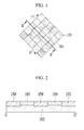
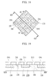
- FIG. 1 is a top plan view showing an exemplary embodiment of a pattern structure of a doping region in a solar cell according to the present invention.
- FIG. 2 is a cross-sectional view taken along line II-II' of FIG. 1 .
- a first doping region 150 and a second doping region 160 are disposed on a surface of a substrate 100.
- the substrate 100 may be an N-type silicon wafer.
- polarities of an impurity region and the doping regions of the exemplary embodiment may be changed to be applied to a P-type wafer.
- the first doping region 150 and the second doping region 160 are alternately arranged with a grid pattern.
- a first unit which refers to one first doping region 150 and one second doping region 160 that neighbor each other is repeatedly arranged along a second direction d2 as well as a first direction d1 where the first direction d1 and the second direction d2 are substantially perpendicular to each other.
- the first doping region 150 and the second doping region 160 may have a quadrangle shape in a viewpoint of a plane area, but not limited thereto, and may have various other shapes.
- the first doping region 150 and the second doping region 160 form a PN conjunction.
- FIG. 3 is a top plan view of the exemplary embodiment of the solar cell of FIG. 1 including an added electrode according to the present invention.
- FIG. 4 is a cross-sectional view taken along line IV-IV' of FIG. 3 .
- a passivation layer 170 disposed on the first doping region 150 and the second doping region 160 is disposed on the substrate 100.
- the passivation layer 170 has a plurality of first contact holes CH1 and a plurality of second contact holes CH2.
- the plurality of first contact holes CH1 is positioned corresponding to the first doping region 150, and the plurality of second contact holes CH2 is positioned corresponding to the second doping region 160.
- a first electrode and a second electrode are disposed on the passivation layer 170.
- the first electrode includes a first grid electrode 180 and a first grid electrode line 181 extending from the first grid electrode 180.
- the second electrode includes a second grid electrode 190 and a second grid electrode line 191 extending from the second grid electrode 190.
- the first grid electrode line 181 fills the plurality of the first contact hole CH1, and the second grid electrode line 191 fills the plurality of the second contact hole CH2.
- first grid electrode line 181 is connected to the first doping region 150 through the plurality of the first contact hole CH1
- second grid electrode line 191 is connected to the second doping region 160 through the plurality of the second contact hole CH2.
- the first grid electrode 180 connects at least two of the first grid electrode lines 181, and the second grid electrode 190 connects at least two of the second grid electrode lines 191.
- the first grid electrode 180 and the second grid electrode 190 face each other and extend substantially perpendicular to a third direction d3.
- the first grid electrode line 181 extends according to the third direction d3 forming an angle of about 45 degrees with at least one of the first direction d1 and the second direction d2.
- the second grid electrode line 191 extends in the opposite direction to the third direction d3 and is substantially parallel to the first grid electrode line 181.
- the first grid electrode line 181 and the second grid electrode line 191 extend with a substantially straight line shape.
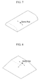
- FIGS. 5 and 6 are top plan views to compare moving distances of a carrier according to a pattern structure of a doping region.
- FIG. 5 shows a doping region having an n+ region and a p+ region with a stripe pattern in the surface of a wafer substrate.
- the P+ region of the stripe pattern has a width W A .
- electron carriers generated by light may be moved by potential of the p+ region and the n+ region.
- an electron E denoted in FIG. 5 moves according to an arrow direction toward the n+ region, and the movement distance is denoted by D A .
- an electron having a short lifetime is recombined before movement of the movement distance D A such that it does not contribute to light efficiency.
- FIG. 6 is a view showing an exemplary embodiment of a pattern structure of a doping region in a solar cell according to the present invention.
- the p+ region 150 i.e., the first doping region
- the n+ region 160 i.e., the second doping region
- the p+ region has a width W B in the second direction d2.
- the width W B in the second direction d2 may be equal to the width W B of the first direction d1.
- the electron E denoted in FIG. 6 must be moved into the n+ region.
- the carrier may be moved in one direction with a shortest distance when the solar cell includes the doping regions of the stripe pattern as shown in FIG. 5 , however, in the exemplary embodiment according to the present invention, the carrier may be moved along the shortest distance D B of the first direction d1 that is shorter than the distance D A of the second direction d2 when the doping regions are alternately arranged with the lattice shape.
- the movement distance of the carrier may be shortened in terms of probability in the exemplary embodiment that the doping regions are alternately arranged with the lattice shape compared with the stripe pattern such that the carrier having the short lifetime may be collected, and thereby a light efficiency may be substantially increased under a same light irradiation condition.
- FIGS. 7 and 8 are band diagrams to compare an electric field applied to carriers according to a pattern structure of a doping region.
- FIG. 7 shows an electric field applied to an electron carrier generated by the light in the case of having the pattern structure of FIG. 5
- FIG. 8 shows an electric field applied to an electron carrier generated by the light in the exemplary embodiment having the pattern structure of FIG. 6 .
- the electron carrier of FIG. 7 is operated by the electric field in one direction.
- the electron carrier of FIG. 8 receives the effect of the electric field in all directions such that effective carrier correction is further possible.
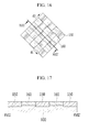
- FIG. 9 is a top plan view showing another exemplary embodiment of an electrode structure in a solar cell according the present invention.
- FIG. 9 The exemplary embodiment of FIG. 9 is substantially the same as the exemplary embodiment described with reference to FIGS. 3 and 4 .
- a shape of grid electrode lines 271 and 281 connected to doping regions 210 and 220 through contact holes CH3 and CH4 formed in a passivation layer 250 is different from the shape of grid electrode lines of FIGS. 3 and 4 .
- the third grid electrode line 271 extends from a third grid electrode 270, and the fourth grid electrode line 281 extends from a fourth grid electrode 280.
- the third grid electrode line 271 and the fourth grid electrode line 281 include a portion extending in a zigzag shape.
- the third grid electrode 270 the and fourth grid electrode line 281 extend substantially parallel to the first direction d1 and the third doping region 210 and the fourth doping region 220 are alternately arranged, thereby forming a structure of the grid electrode lines 271 and 281 substantially similar to a zigzag shape.
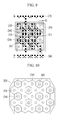
- FIG. 10 is a top plan view showing another exemplary embodiment of a pattern structure of a doping region in a solar cell according to the present invention.
- a sixth doping region 380 enclosed by a fifth doping region 370 and the fifth doping region 370 having a substantially wide area and formed with an island shape are positioned in a surface of the substrate.
- a passivation layer 350 disposed on the fifth doping region 370 and the sixth doping region 380 is positioned on the substrate, and the passivation layer 350 has a plurality of fifth contact holes CH5 and a plurality of sixth contact holes CH6.
- the plurality of fifth contact holes CH5 is formed at uniform intervals and is formed at positions corresponding to the fifth doping region 370, and the plurality of sixth contact holes CH6 is formed at uniform intervals and are formed at positions corresponding to the sixth doping region 380.
- the fifth doping region 370 and a fifth grid electrode line may be connected though the fifth contact hole CH5, and the sixth doping region 380 and a sixth grid electrode line (not shown) may be connected through the sixth contact hole CH6.
- FIGS. 11 to 19 are plan views and cross-sectional views showing a manufacturing method of the exemplary embodiment of the solar cell of FIG. 1 .
- a first doping layer 110 is deposited on a substrate 100, and a diffusion preventing layer 120 is disposed on the first doping layer 110.
- the first doping layer 110 and the diffusion preventing layer 120 are patterned to partially expose a surface of the substrate 100.
- a portion corresponding to the exposed surface of the substrate 100 and a portion of the remaining first doping layer 110 and diffusion preventing layer 120 that are not patterned are alternately arranged with a lattice shape in a plane view.
- the patterning of the first doping layer 110 and the diffusion preventing layer 120 may include at least one of a photolithography process, a screen printing process including an etching paste, or an inkjet printing process, for example, but is not limited thereto and may include various other processes.
- the first doping layer 110 may include a silicon oxide doped with the P-type impurity.
- the silicon oxide may be silicon dioxide (SiO2), for example.
- the P-type impurity may be boron (B), gallium (Ga), or indium (In), for example, but is not limited thereto and may include other materials with similar characteristics.
- the substrate 100 includes a front side and a back side opposing the front side.
- the first doping layer 110 is formed on the back side of the substrate 100.
- the front side of the substrate 100 is a surface where light is absorbed from an outside.
- the diffusion preventing layer 120 may include the silicon oxide that is not doped.
- a second doping layer 140 disposed on the exposed portion of the substrate 100 is disposed on the diffusion preventing layer 120.
- the second doping layer 140 may include the silicon oxide doped with the N-type impurity.
- the silicon oxide may be silicon dioxide (SiO2), for example.
- the N-type impurity may be phosphorus (P), arsenic (As), or other materials with similar characteristics.
- a heat treatment process is executed to diffuse an impurity from the first doping layer 110 such that a first doping region 150 is formed.
- the impurity is diffused from the second doping layer 140 contacting the substrate 100 such that a second doping region 160 is formed.
- the first doping region 150 and the second doping region 160 may be substantially simultaneously formed.
- the second doping layer 140 may not be disposed, and impurity ions may be injected into the surface of the substrate 100 using the first doping layer 110 and the diffusion preventing layer 120 as a mask.
- the impurity ions are injected into the surface of the substrate 100 using the first doping layer 110 and the diffusion preventing layer 120 as a mask.
- the impurity ions may be phosphorus (P), arsenic (As), or other materials with similar characteristics.
- the heat treatment is executed to diffuse the impurity from the first doping layer 110 such that the first doping region 150 is formed, and the impurity injected to the substrate 100 through the ion injection method is activated by the heat treatment such that the second doping region 160 is formed.
- the first doping layer 110, the diffusion preventing layer 120, and the second doping layer 140 formed on the substrate 100 are removed.
- the first doping layer 110, the diffusion preventing layer 120, and the second doping layer 140 may be etched using hydrogen fluoride (HF) having large etching selectivity for the substrate 100, for example, but is not limited thereto and may use various other methods.
- HF hydrogen fluoride
- the first doping region 150 and the second doping region 160 are alternately arranged with the grid pattern.
- first unit one first doping region 150 and one second doping region 160 that neighbor each other is referred to as a first unit, and the first unit is repeatedly arranged according to a second direction d2 as well as a first direction d1, where the first direction d1 and the second direction d2 are substantially perpendicular to each other.
- the first doping region 150 and the second doping region 160 form a PN conjunction.
- a passivation layer 170 having the first contact hole CH1 and the second contact hole CH2 is formed on the first doping region 150 and the second doping region 160, respectively.
- the first electrode including the first grid electrode 180 and the first grid electrode line 181, and the second electrode including the second grid electrode 190 and the second grid electrode line 191, are formed on the passivation layer 170.
- the first grid electrode line 181 extends according to the third direction d3 with the straight line shape to be connected to the first doping region 150 through the first contact hole CH1.
- the second grid electrode line 191 extends according to the third direction d3 with the straight line shape to be connected to the second doping region 160 through the second contact hole CH2.
Landscapes
- Photovoltaic Devices (AREA)
Applications Claiming Priority (1)
| Application Number | Priority Date | Filing Date | Title |
|---|---|---|---|
| KR1020100069495A KR101702982B1 (ko) | 2010-07-19 | 2010-07-19 | 태양 전지 및 그 제조 방법 |
Publications (1)
| Publication Number | Publication Date |
|---|---|
| EP2410568A2 true EP2410568A2 (fr) | 2012-01-25 |
Family
ID=45090841
Family Applications (1)
| Application Number | Title | Priority Date | Filing Date |
|---|---|---|---|
| EP11154459A Withdrawn EP2410568A2 (fr) | 2010-07-19 | 2011-02-15 | Cellule solaire et son procédé de fabrication |
Country Status (5)
| Country | Link |
|---|---|
| US (1) | US20120012173A1 (fr) |
| EP (1) | EP2410568A2 (fr) |
| JP (1) | JP5873646B2 (fr) |
| KR (1) | KR101702982B1 (fr) |
| CN (1) | CN102339873B (fr) |
Cited By (2)
| Publication number | Priority date | Publication date | Assignee | Title |
|---|---|---|---|---|
| EP2854183A1 (fr) * | 2013-09-25 | 2015-04-01 | Inventec Solar Energy Corporation | Cellule solaire à contact arrière |
| US20210018364A1 (en) * | 2018-03-30 | 2021-01-21 | Centre National De La Recherche Scientifique | Generation and detection of terahertz radiation with an arbitrary polarization direction |
Families Citing this family (12)
| Publication number | Priority date | Publication date | Assignee | Title |
|---|---|---|---|---|
| US9190548B2 (en) * | 2011-10-11 | 2015-11-17 | Varian Semiconductor Equipment Associates, Inc. | Method of creating two dimensional doping patterns in solar cells |
| CN103378205A (zh) * | 2012-04-13 | 2013-10-30 | 杜邦太阳能有限公司 | 太阳能模组 |
| US20140130854A1 (en) * | 2012-11-12 | 2014-05-15 | Samsung Sdi Co., Ltd. | Photoelectric device and the manufacturing method thereof |
| TWI476940B (zh) * | 2012-12-28 | 2015-03-11 | Motech Ind Inc | 太陽能電池與太陽能電池模組 |
| TWI500174B (zh) * | 2013-01-08 | 2015-09-11 | Motech Ind Inc | 太陽能電池及其模組 |
| TWI483411B (zh) * | 2013-02-20 | 2015-05-01 | Motech Ind Inc | 太陽能電池及其模組 |
| US9246046B1 (en) * | 2014-09-26 | 2016-01-26 | Sunpower Corporation | Etching processes for solar cell fabrication |
| WO2016158977A1 (fr) * | 2015-03-31 | 2016-10-06 | 株式会社カネカ | Batterie solaire et module de batterie solaire |
| CN114361266B (zh) * | 2020-09-28 | 2024-03-22 | 苏州阿特斯阳光电力科技有限公司 | 光伏组件 |
| AU2021371440A1 (en) * | 2020-10-29 | 2023-03-02 | Newsouth Innovations Pty Limited | A solar cell structure and a method of forming a solar cell structure |
| CN118156325A (zh) | 2022-12-07 | 2024-06-07 | 浙江晶科能源有限公司 | 太阳能电池及光伏组件 |
| CN117637874B (zh) * | 2024-01-26 | 2024-06-21 | 隆基绿能科技股份有限公司 | 一种背接触电池及其制造方法 |
Family Cites Families (8)
| Publication number | Priority date | Publication date | Assignee | Title |
|---|---|---|---|---|
| US5538564A (en) | 1994-03-18 | 1996-07-23 | Regents Of The University Of California | Three dimensional amorphous silicon/microcrystalline silicon solar cells |
| JP4831272B2 (ja) * | 2001-03-26 | 2011-12-07 | 株式会社デンソー | 半導体装置の製造方法 |
| JP5142980B2 (ja) * | 2006-03-01 | 2013-02-13 | 三洋電機株式会社 | 太陽電池セル、及び、この太陽電池セルを用いた太陽電池モジュール |
| EP2654089A3 (fr) * | 2007-02-16 | 2015-08-12 | Nanogram Corporation | Structures de cellules solaires, modules photovoltaïques et procédés correspondants |
| CN101874304B (zh) | 2007-11-22 | 2012-07-18 | 夏普株式会社 | 元件间布线构件、光电转换元件及使用其的光电转换元件连接体和光电转换组件 |
| JP2009158519A (ja) * | 2007-12-25 | 2009-07-16 | Toyota Motor Corp | 半導体装置及びその製造方法 |
| JP2009188355A (ja) * | 2008-02-08 | 2009-08-20 | Sanyo Electric Co Ltd | 太陽電池 |
| JP5546759B2 (ja) * | 2008-08-05 | 2014-07-09 | トヨタ自動車株式会社 | 半導体装置及びその製造方法 |
-
2010
- 2010-07-19 KR KR1020100069495A patent/KR101702982B1/ko not_active Expired - Fee Related
-
2011
- 2011-02-15 EP EP11154459A patent/EP2410568A2/fr not_active Withdrawn
- 2011-02-16 US US13/028,697 patent/US20120012173A1/en not_active Abandoned
- 2011-05-17 JP JP2011110051A patent/JP5873646B2/ja not_active Expired - Fee Related
- 2011-07-13 CN CN201110195544.4A patent/CN102339873B/zh not_active Expired - Fee Related
Non-Patent Citations (1)
| Title |
|---|
| None |
Cited By (3)
| Publication number | Priority date | Publication date | Assignee | Title |
|---|---|---|---|---|
| EP2854183A1 (fr) * | 2013-09-25 | 2015-04-01 | Inventec Solar Energy Corporation | Cellule solaire à contact arrière |
| US20210018364A1 (en) * | 2018-03-30 | 2021-01-21 | Centre National De La Recherche Scientifique | Generation and detection of terahertz radiation with an arbitrary polarization direction |
| US11808627B2 (en) * | 2018-03-30 | 2023-11-07 | Centre National De La Recherche Scientifique | Generation and detection of terahertz radiation with an arbitrary polarization direction |
Also Published As
| Publication number | Publication date |
|---|---|
| CN102339873B (zh) | 2016-06-15 |
| KR101702982B1 (ko) | 2017-02-06 |
| US20120012173A1 (en) | 2012-01-19 |
| JP2012028742A (ja) | 2012-02-09 |
| KR20120009576A (ko) | 2012-02-02 |
| JP5873646B2 (ja) | 2016-03-01 |
| CN102339873A (zh) | 2012-02-01 |
Similar Documents
| Publication | Publication Date | Title |
|---|---|---|
| EP2410568A2 (fr) | Cellule solaire et son procédé de fabrication | |
| JP5999382B2 (ja) | ベース拡散エリアを小さくした太陽電池 | |
| EP2993703B1 (fr) | Cellule solaire et son procédé de fabrication | |
| US9214593B2 (en) | Solar cell and method for manufacturing the same | |
| KR101258938B1 (ko) | 태양 전지 | |
| US9929294B2 (en) | Photoelectric conversion device, manufacturing method thereof, and photoelectric conversion module | |
| US20120180860A1 (en) | Solar cell and method for manufacturing the same | |
| US8269258B2 (en) | Method for manufacturing a solar cell | |
| KR101757877B1 (ko) | 태양 전지 및 그의 제조 방법 | |
| KR20140022508A (ko) | 후면전극형 이종접합 태양전지의 제조방법 | |
| KR101348848B1 (ko) | 후면전극형 태양전지의 제조방법 | |
| US8633375B2 (en) | Solar cell and method for Manufacturing the same | |
| KR20160031818A (ko) | 태양 전지 | |
| KR101798967B1 (ko) | 태양 전지의 제조 방법 | |
| KR101335195B1 (ko) | 후면전극형 태양전지 및 그 제조방법 | |
| KR101153378B1 (ko) | 플로팅 접합을 이용한 후면전극 태양전지 및 그 제조방법 | |
| KR101833936B1 (ko) | 태양 전지 및 그 제조 방법 | |
| JP2014067870A (ja) | 太陽電池およびその製造方法 | |
| KR101854237B1 (ko) | 태양전지 및 그 제조방법 | |
| KR101736960B1 (ko) | 태양 전지 및 그 제조 방법 | |
| JP2017037899A (ja) | 太陽電池セル |
Legal Events
| Date | Code | Title | Description |
|---|---|---|---|
| AK | Designated contracting states |
Kind code of ref document: A2 Designated state(s): AL AT BE BG CH CY CZ DE DK EE ES FI FR GB GR HR HU IE IS IT LI LT LU LV MC MK MT NL NO PL PT RO RS SE SI SK SM TR |
|
| AX | Request for extension of the european patent |
Extension state: BA ME |
|
| PUAI | Public reference made under article 153(3) epc to a published international application that has entered the european phase |
Free format text: ORIGINAL CODE: 0009012 |
|
| RAP1 | Party data changed (applicant data changed or rights of an application transferred) |
Owner name: SAMSUNG ELECTRONICS CO., LTD. Owner name: SAMSUNG SDI CO., LTD. |
|
| STAA | Information on the status of an ep patent application or granted ep patent |
Free format text: STATUS: THE APPLICATION HAS BEEN WITHDRAWN |
|
| 18W | Application withdrawn |
Effective date: 20130321 |