EP2854183A1 - Cellule solaire à contact arrière - Google Patents
Cellule solaire à contact arrière Download PDFInfo
- Publication number
- EP2854183A1 EP2854183A1 EP14151032.1A EP14151032A EP2854183A1 EP 2854183 A1 EP2854183 A1 EP 2854183A1 EP 14151032 A EP14151032 A EP 14151032A EP 2854183 A1 EP2854183 A1 EP 2854183A1
- Authority
- EP
- European Patent Office
- Prior art keywords
- emitter
- base
- solar cell
- back contact
- diffusion region
- Prior art date
- Legal status (The legal status is an assumption and is not a legal conclusion. Google has not performed a legal analysis and makes no representation as to the accuracy of the status listed.)
- Withdrawn
Links
- 238000009792 diffusion process Methods 0.000 claims abstract description 131
- 239000011449 brick Substances 0.000 claims abstract description 10
- 239000002800 charge carrier Substances 0.000 claims description 26
- XUIMIQQOPSSXEZ-UHFFFAOYSA-N Silicon Chemical compound [Si] XUIMIQQOPSSXEZ-UHFFFAOYSA-N 0.000 claims description 10
- 229910052710 silicon Inorganic materials 0.000 claims description 10
- 239000010703 silicon Substances 0.000 claims description 10
- 239000000969 carrier Substances 0.000 description 10
- 238000006243 chemical reaction Methods 0.000 description 5
- 238000004519 manufacturing process Methods 0.000 description 3
- 230000006798 recombination Effects 0.000 description 3
- 238000005215 recombination Methods 0.000 description 3
- 230000005540 biological transmission Effects 0.000 description 2
- 238000000034 method Methods 0.000 description 2
- 239000004065 semiconductor Substances 0.000 description 2
- 239000011248 coating agent Substances 0.000 description 1
- 238000000576 coating method Methods 0.000 description 1
- 238000005530 etching Methods 0.000 description 1
- 238000009434 installation Methods 0.000 description 1
- 230000000873 masking effect Effects 0.000 description 1
- 239000007769 metal material Substances 0.000 description 1
- 238000012986 modification Methods 0.000 description 1
- 230000004048 modification Effects 0.000 description 1
Images


Classifications
-
- H—ELECTRICITY
- H10—SEMICONDUCTOR DEVICES; ELECTRIC SOLID-STATE DEVICES NOT OTHERWISE PROVIDED FOR
- H10F—INORGANIC SEMICONDUCTOR DEVICES SENSITIVE TO INFRARED RADIATION, LIGHT, ELECTROMAGNETIC RADIATION OF SHORTER WAVELENGTH OR CORPUSCULAR RADIATION
- H10F10/00—Individual photovoltaic cells, e.g. solar cells
- H10F10/10—Individual photovoltaic cells, e.g. solar cells having potential barriers
- H10F10/11—Photovoltaic cells having point contact potential barriers
-
- H—ELECTRICITY
- H10—SEMICONDUCTOR DEVICES; ELECTRIC SOLID-STATE DEVICES NOT OTHERWISE PROVIDED FOR
- H10F—INORGANIC SEMICONDUCTOR DEVICES SENSITIVE TO INFRARED RADIATION, LIGHT, ELECTROMAGNETIC RADIATION OF SHORTER WAVELENGTH OR CORPUSCULAR RADIATION
- H10F77/00—Constructional details of devices covered by this subclass
- H10F77/20—Electrodes
- H10F77/206—Electrodes for devices having potential barriers
- H10F77/211—Electrodes for devices having potential barriers for photovoltaic cells
- H10F77/215—Geometries of grid contacts
-
- H—ELECTRICITY
- H10—SEMICONDUCTOR DEVICES; ELECTRIC SOLID-STATE DEVICES NOT OTHERWISE PROVIDED FOR
- H10F—INORGANIC SEMICONDUCTOR DEVICES SENSITIVE TO INFRARED RADIATION, LIGHT, ELECTROMAGNETIC RADIATION OF SHORTER WAVELENGTH OR CORPUSCULAR RADIATION
- H10F77/00—Constructional details of devices covered by this subclass
- H10F77/20—Electrodes
- H10F77/206—Electrodes for devices having potential barriers
- H10F77/211—Electrodes for devices having potential barriers for photovoltaic cells
- H10F77/219—Arrangements for electrodes of back-contact photovoltaic cells
-
- Y—GENERAL TAGGING OF NEW TECHNOLOGICAL DEVELOPMENTS; GENERAL TAGGING OF CROSS-SECTIONAL TECHNOLOGIES SPANNING OVER SEVERAL SECTIONS OF THE IPC; TECHNICAL SUBJECTS COVERED BY FORMER USPC CROSS-REFERENCE ART COLLECTIONS [XRACs] AND DIGESTS
- Y02—TECHNOLOGIES OR APPLICATIONS FOR MITIGATION OR ADAPTATION AGAINST CLIMATE CHANGE
- Y02E—REDUCTION OF GREENHOUSE GAS [GHG] EMISSIONS, RELATED TO ENERGY GENERATION, TRANSMISSION OR DISTRIBUTION
- Y02E10/00—Energy generation through renewable energy sources
- Y02E10/50—Photovoltaic [PV] energy
Definitions
- the present invention relates to a solar cell, and more particularly relates to a back contact solar cell, which can shorten a path for collecting carriers.
- the electrode members which are used to be disposed on the top side, are disposed on the back side now, thus the area where the electrode members shading on the top side is reduced and the photovoltaic conversion efficiency of the back contact solar cell is enhanced.
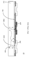
- FIG. 1 is a sectional view of a conventional back contact solar cell.
- the conventional back contact solar cell 10 includes a silicon wafer 102, a base diffusion region 104, and an emitter diffusion region 106.
- the base electrode member 108 is electrically connected with the base diffusion region 104 from the base contacts 1042. Therefore, the majority charge carriers (electrons) collected in the base diffusion region 104 can be transmitted to an external circuit from the base electrode members 108.
- the emitter electrode member 109 is electrically connected with the emitter diffusion region 106 from the emitter contacts 1062. Therefore, the minority charge carriers (electron holes) collected in the emitter diffusion region 106 can be transmitted to the external circuit from the emitter electrode members 109.
- the carriers are mostly generated on the top side of the solar cell, and the majority carriers or the minority carriers are requested to travel from the generation points to the back side.
- the path which the carriers travel is called a carrier path.
- the traveling path for collecting the carriers can be shortened to reduce the recombination loss of the minority charge carriers, or the serial resistance loss caused by the horizontal flowing of the majority charge carriers, so as to enhance the conversion efficiency of the solar cell. Accordingly, the traveling path for collecting the carriers is a significant factor in determining the capability of the back contact solar cell 10.
- One objective of the present invention is to provide a structure of a back contact solar cell to shorten the traveling path to collect carriers so as to enhance the capability of the solar cell.
- a back contact solar cell includes a base diffusion region, a plurality of emitter diffusion regions, and a plurality of base electrodes.
- the base diffusion region forms a plurality of openings thereon, and each of the emitter diffusion regions is a brick pattern structure disposed within the openings of the base diffusion region and surrounded by the base diffusion region.
- the base contacts are disposed on the base diffusion region and located between the emitter diffusion regions. Each of the emitter contacts is disposed at central position in each of the emitter diffusion regions.
- Another objective of the present invention is to provide a structure of a back contact solar cell to speed up the transmission of the majority charge carrier or the minority charge carrier so as to reduce the recombination loss of the minority charge carriers, or the serial resistance loss caused by the horizontal flowing of the majority charge carriers, and enhance the conversion efficiency of the solar cell.
- a back contact solar cell includes a silicon wafer, a base diffusion region, a plurality of emitter diffusion regions, an insulated layer, a plurality of base contacts, and a plurality of emitter contacts.
- the base diffusion region is disposed on the back side of the silicon wafer, and forms a plurality of openings thereon.
- the emitter diffusion regions are disposed on the back side of the silicon wafer and respectively disposed within the openings.
- Each of the emitter diffusion regions is a brick pattern structure and surrounded by the base diffusion region.
- the insulated layer is disposed on top of the base diffusion region and the emitter diffusion regions.
- the base contacts are disposed on the base diffusion region and located between the emitter diffusion regions. Each of the emitter contacts is disposed at a central position in each of the emitter diffusion regions.
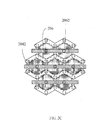
- FIG. 2A is a view of a back contact solar cell illustrated in one embodiment of the present invention.
- the back contact solar cell 20 includes a solar wafer 202, a base diffusion region 204, and a plurality of emitter diffusion regions 206.
- the base diffusion region 204 and the emitter diffusion regions 206 are disposed on the back side of the solar wafer 202.
- Each of the emitter diffusion regions 206 is a brick pattern structure, and the base diffusion region 204 surrounds the brick pattern structure of the emitter diffusion region 206.
- the emitter diffusion regions 206 are arranged as multiple columns, and every two columns of the adjacent emitter diffusion regions 206 are aligned to each other.
- each of the base contacts 2042 is disposed on the base diffusion region 204, and the disposing position of each of the base contacts 2042 is preferred to be in a corner close to each of the emitter diffusion regions 206 to have a larger alignment space during the manufacturing process.
- the disposing position for each of the base contacts 2042 can be in any locations on the base diffusion region 204, and it is not limited herein.
- the base contact 2042 is not limited to being designed as a circular or rectangular shape.
- Each of the emitter contacts 2062 is disposed within the brick pattern structure of each of the emitter diffusion regions 206, and is preferably at the center of the brick pattern. The intervals between every two of the emitter contacts 2062 are the same. However, in a different embodiment, in order to optimize the contact resistance, the emitter contacts 2062 can be a plurality of circular shaped contacts, rectangular shaped contacts, or any other shape contacts. As the example shown in FIG. 2A , in one embodiment of the present invention, for one 400um X 400um unit of the silicon wafer, each of the emitter diffusion regions 206 is a square-like brick pattern structure about 350um wide.
- the four corners of the square pattern are shrunk a little to reserve a larger space of the base diffusion region to arrange the base contacts 2042, and the width of the base diffusion region at the location of the corner is a small square shape about 140um wide.
- the minimum width of the base diffusion region 204 between the two emitter diffusion regions is about 50 um wide and the width of the base contacts 2052 and the width of the emitter contacts 2062 are 60um and 80um respectively.
- the base diffusion regions 204, the emitter diffusion regions 206, the base contacts 2042, and the emitter contacts 2062 can be made by the semiconductor process, such as deposing, coating, masking, laser, etching, and so on, and those semiconductor processes are well known to a person with ordinary skill in the art and the description thereof is omitted herein.
- a carrier A and a carrier B are disposed on the back contact electrode member.
- the carrier A is a minority charge carrier and the carrier A can reach the emitter diffusion region 206 from an up, down, right or left direction. Therefore, the carrier A can have the shortest path to reach the emitter diffusion region 206.
- the carrier B is a majority charge carrier and the carrier B can also reach the base diffusion region 205 from the up, down, right or left direction. Therefore, the carrier B can have the shortest path to reach the base diffusion region 204.
- the majority charge carriers or the minority charge carriers can find the shortest path to reach the base diffusion region 204 or the emitter diffusion region 206.
- the best path can only be found from the right or left direction or the up or down direction. The transmitting efficiency of the carriers in the back contact solar cell of the present invention is much better.
- FIG. 2B is a view of the electrode layout of the back contact solar cell in the embodiment of the present invention.
- the base diffusion region 204 after the installation of the base diffusion region 204, the emitter diffusion region 206, the base contacts 2042 and the emitter contacts 2062, in order for the collected majority carrier able to be transmitted to the external circuit from the base diffusion region 205, there are multiple base electrode members 208 disposed on the base contacts 2042.
- the base electrode members 208 are long strip shapes, and are electrically connected with the base diffusion region 204 by each of the base contacts 2042. Subsequently, the base electrode member 208 is electrically connected with the external circuit, and the majority charge carriers (electrons) collected in the base diffusion region 204 can be transmitted to the external circuit.
- the emitter electrode members 209 there are multiple emitter electrode members 209 disposed on the emitter contacts 2062.
- the emitter electrode members 209 are also long strip shapes, and are electrically connected with the emitter diffusion region 206 by the emitter contacts 2062. Therefore, the minority charge carrier 209 (electron holes) collected in the emitter diffusion region 206 can be transmitted to the external circuit.
- the base electrode members 208 and the emitter electrode member 209 are pin-like structures, and the base electrode members 208 and the emitter electrode members 209 are directly and electrically connected with the base diffusion region 204 and the emitter diffusion region 206 from the base contacts 2042 and the emitter contacts 2062 by those pins, and it is not limited herein.
- the base electrode members 208 and the emitter electrode members 209 are paralleled to each other, and there is an insulated layer disposed between the base electrode members 208 and the emitter diffusion region 206, or the base electrode members 208 and the emitter electrode members 209, to prevent the base electrode members 208 and the emitter electrode members 209 from being electrically contacted.
- the arrangement pattern or shape of the emitter diffusion region 206 can be different from the emitter diffusion region 206 shown in FIG. 2A .
- all of the emitter diffusion regions 206 are circularly shaped, and every two columns of the adjacent emitter diffusion regions 206 can be misaligned to each other.
- the base electrode member 208 can be arranged in a sawtooth-like shape.
- the emitter diffusion regions 206 are hexagon shaped, and the base electrode members 208 are arranged between the two emitter diffusion regions 206.
- the base electrode members 208 are also arranged in a sawtooth-like shape. In the embodiment shown in FIG.
- the emitter diffusion regions 206 are triangular shapes, and the base electrode members 208 are long strip shapes, and the emitter electrode members 209 are arranged in a sawtooth-like shape.
- the base electrode regions 206 of the present invention can be shown in different shapes in accordance with the different embodiments.
- the base electrode members 208 are not always arranged as long strip shapes to let the majority charge carriers or the minority charge carriers find the best path to reach the base diffusion region 204 or the emitter diffusion region 206.
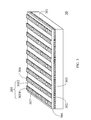
- FIG. 3 is a three-dimensional sectional view of the back contact solar cell in the embodiment of the present invention.
- the back side of the solar cell 30 in FIG. 3 is on the top.
- the bottom layer is a silicon wafer 301
- the top of the silicon wafer 301 is a base diffusion region 302.
- emitter diffusion regions 303 are disposed on the openings
- an insulated layer 304 is disposed on the base diffusion region 302 and the emitter diffusion regions 303.
- the contacts 305 on the insulated layer 304 to expose the base diffusion region 302 are base contacts 3052, and the contacts 305 on the insulated layer 304 to expose the emitter diffusion regions 303 are emitter contacts 3054. Thereafter, multiple base electrode members 306 with long strip shapes are disposed on the base contacts 3052, and the multiple emitter electrode members 307 with long strip shapes are disposed on the emitter contacts 3054. It is obvious to see in figures that the base electrode members 306 and the emitter electrode members 307 are not electrically connected with the emitter diffusion region 303 and the base diffusion region 302 at the bottom because of the insulated layer 304.
- the majority charge carriers or the minority charge carriers can find the shortest path to reach the base diffusion region 302 or the emitter diffusion region 303 so as to speed up the transmission of the majority charge carriers or the minority charge carriers and reduce the recombination loss of the minority charge carriers or the serial resistance loss caused by the horizontal flowing of the majority charge carriers to enhance the conversion efficiency of the solar cell.
Landscapes
- Photovoltaic Devices (AREA)
Applications Claiming Priority (1)
| Application Number | Priority Date | Filing Date | Title |
|---|---|---|---|
| TW102217943U TWM477049U (en) | 2013-09-25 | 2013-09-25 | Back contact electrode solar cell |
Publications (1)
| Publication Number | Publication Date |
|---|---|
| EP2854183A1 true EP2854183A1 (fr) | 2015-04-01 |
Family
ID=49920232
Family Applications (1)
| Application Number | Title | Priority Date | Filing Date |
|---|---|---|---|
| EP14151032.1A Withdrawn EP2854183A1 (fr) | 2013-09-25 | 2014-01-14 | Cellule solaire à contact arrière |
Country Status (2)
| Country | Link |
|---|---|
| EP (1) | EP2854183A1 (fr) |
| TW (1) | TWM477049U (fr) |
Cited By (2)
| Publication number | Priority date | Publication date | Assignee | Title |
|---|---|---|---|---|
| RU2655953C1 (ru) * | 2017-07-07 | 2018-05-30 | Акционерное общество "НПО "Орион" | Способ изготовления микроконтактов |
| AU2025210840B2 (en) * | 2024-01-26 | 2026-03-19 | Longi Green Energy Technology Co., Ltd. | Back contact solar cell and method for manufacturing the same |
Families Citing this family (1)
| Publication number | Priority date | Publication date | Assignee | Title |
|---|---|---|---|---|
| TWI513026B (zh) * | 2014-07-30 | 2015-12-11 | Inventec Solar Energy Corp | 太陽能電池 |
Citations (11)
| Publication number | Priority date | Publication date | Assignee | Title |
|---|---|---|---|---|
| US6034321A (en) * | 1998-03-24 | 2000-03-07 | Essential Research, Inc. | Dot-junction photovoltaic cells using high-absorption semiconductors |
| US20070295399A1 (en) * | 2005-12-16 | 2007-12-27 | Bp Corporation North America Inc. | Back-Contact Photovoltaic Cells |
| US20080017243A1 (en) * | 2006-07-24 | 2008-01-24 | Denis De Ceuster | Solar cell with reduced base diffusion area |
| JP2009188355A (ja) * | 2008-02-08 | 2009-08-20 | Sanyo Electric Co Ltd | 太陽電池 |
| US20110023956A1 (en) * | 2007-12-11 | 2011-02-03 | Nils-Peter Harder | Rear-contact solar cell having extensive rear side emitter regions and method for producing the same |
| EP2410568A2 (fr) * | 2010-07-19 | 2012-01-25 | Samsung Electronics Co., Ltd. | Cellule solaire et son procédé de fabrication |
| US20120171804A1 (en) * | 2004-11-30 | 2012-07-05 | Solexel, Inc. | Patterning of silicon oxide layers using pulsed laser ablation |
| US20120190183A1 (en) * | 2011-01-24 | 2012-07-26 | Varian Semiconductor Equipment Associates, Inc. | Using multiple masks to form independent features on a workpiece |
| US20130087189A1 (en) * | 2011-10-11 | 2013-04-11 | Varian Semiconductor Equipment Associates, Inc. | Method of creating two dimensional doping patterns in solar cells |
| EP2602834A1 (fr) * | 2010-08-03 | 2013-06-12 | Sharp Kabushiki Kaisha | Cellule solaire |
| KR20130089051A (ko) * | 2012-02-01 | 2013-08-09 | 현대중공업 주식회사 | 후면전극형 태양전지 및 그 제조방법 |
-
2013
- 2013-09-25 TW TW102217943U patent/TWM477049U/zh not_active IP Right Cessation
-
2014
- 2014-01-14 EP EP14151032.1A patent/EP2854183A1/fr not_active Withdrawn
Patent Citations (11)
| Publication number | Priority date | Publication date | Assignee | Title |
|---|---|---|---|---|
| US6034321A (en) * | 1998-03-24 | 2000-03-07 | Essential Research, Inc. | Dot-junction photovoltaic cells using high-absorption semiconductors |
| US20120171804A1 (en) * | 2004-11-30 | 2012-07-05 | Solexel, Inc. | Patterning of silicon oxide layers using pulsed laser ablation |
| US20070295399A1 (en) * | 2005-12-16 | 2007-12-27 | Bp Corporation North America Inc. | Back-Contact Photovoltaic Cells |
| US20080017243A1 (en) * | 2006-07-24 | 2008-01-24 | Denis De Ceuster | Solar cell with reduced base diffusion area |
| US20110023956A1 (en) * | 2007-12-11 | 2011-02-03 | Nils-Peter Harder | Rear-contact solar cell having extensive rear side emitter regions and method for producing the same |
| JP2009188355A (ja) * | 2008-02-08 | 2009-08-20 | Sanyo Electric Co Ltd | 太陽電池 |
| EP2410568A2 (fr) * | 2010-07-19 | 2012-01-25 | Samsung Electronics Co., Ltd. | Cellule solaire et son procédé de fabrication |
| EP2602834A1 (fr) * | 2010-08-03 | 2013-06-12 | Sharp Kabushiki Kaisha | Cellule solaire |
| US20120190183A1 (en) * | 2011-01-24 | 2012-07-26 | Varian Semiconductor Equipment Associates, Inc. | Using multiple masks to form independent features on a workpiece |
| US20130087189A1 (en) * | 2011-10-11 | 2013-04-11 | Varian Semiconductor Equipment Associates, Inc. | Method of creating two dimensional doping patterns in solar cells |
| KR20130089051A (ko) * | 2012-02-01 | 2013-08-09 | 현대중공업 주식회사 | 후면전극형 태양전지 및 그 제조방법 |
Cited By (2)
| Publication number | Priority date | Publication date | Assignee | Title |
|---|---|---|---|---|
| RU2655953C1 (ru) * | 2017-07-07 | 2018-05-30 | Акционерное общество "НПО "Орион" | Способ изготовления микроконтактов |
| AU2025210840B2 (en) * | 2024-01-26 | 2026-03-19 | Longi Green Energy Technology Co., Ltd. | Back contact solar cell and method for manufacturing the same |
Also Published As
| Publication number | Publication date |
|---|---|
| TWM477049U (en) | 2014-04-21 |
Similar Documents
| Publication | Publication Date | Title |
|---|---|---|
| JP6837036B2 (ja) | ベース拡散エリアを小さくした太陽電池および該製造方法 | |
| EP2894676B1 (fr) | Réseau de cellules solaires ayant deux types différents de cellules | |
| US9960292B2 (en) | Radially arranged metal contact fingers for solar cells | |
| KR102195406B1 (ko) | 핀펫과 로컬 인터커넥트 층을 포함하는 반도체 장치 및 그 제조 방법 | |
| US20110139241A1 (en) | Solar cell and method for producing a solar cell | |
| TWI603493B (zh) | 太陽能電池及其模組 | |
| KR20170124639A (ko) | 태양 전지의 제조를 위한 공정 및 구조물 | |
| EP2854183A1 (fr) | Cellule solaire à contact arrière | |
| WO2014163491A1 (fr) | Ensemble de cellules photovoltaïques et procédé de fabrication d'un tel ensemble | |
| JP7001162B2 (ja) | 半導体装置、パワーモジュール及び半導体装置の製造方法 | |
| CN108258030A (zh) | Igbt半导体结构 | |
| US20150114459A1 (en) | Electrode structure and solar cell using the same | |
| JP6095698B2 (ja) | パワー半導体における電流センサのための半導体装置 | |
| CN221201182U (zh) | 无掺杂连接结构及单元 | |
| CN210640236U (zh) | 存储器及其衬垫结构 | |
| CN203491272U (zh) | 背接触电极太阳能电池 | |
| US20210135003A1 (en) | Single-chip containing porous-wafer battery and device and method of making the same | |
| JPWO2017038733A1 (ja) | 光電変換素子 | |
| KR20160098915A (ko) | 수직형 베타전지 구조체 및 그 제조방법 | |
| CN103515424A (zh) | 半导体器件及其制造方法 | |
| CN103956349B (zh) | 功率半导体芯片的铜金属化结构及其制作方法 | |
| CN110112274B (zh) | 垂直结构芯片及制作方法 | |
| CN119153537A (zh) | 半导体器件和半导体器件的制作方法 | |
| CN112885805A (zh) | 存储器、存储器的衬垫结构及其制备方法 | |
| TW202332065A (zh) | 指叉型變容二極體及其製作方法 |
Legal Events
| Date | Code | Title | Description |
|---|---|---|---|
| PUAI | Public reference made under article 153(3) epc to a published international application that has entered the european phase |
Free format text: ORIGINAL CODE: 0009012 |
|
| 17P | Request for examination filed |
Effective date: 20140114 |
|
| AK | Designated contracting states |
Kind code of ref document: A1 Designated state(s): AL AT BE BG CH CY CZ DE DK EE ES FI FR GB GR HR HU IE IS IT LI LT LU LV MC MK MT NL NO PL PT RO RS SE SI SK SM TR |
|
| AX | Request for extension of the european patent |
Extension state: BA ME |
|
| RBV | Designated contracting states (corrected) |
Designated state(s): AL AT BE BG CH CY CZ DE DK EE ES FI FR GB GR HR HU IE IS IT LI LT LU LV MC MK MT NL NO PL PT RO RS SE SI SK SM TR |
|
| 17Q | First examination report despatched |
Effective date: 20171023 |
|
| STAA | Information on the status of an ep patent application or granted ep patent |
Free format text: STATUS: THE APPLICATION IS DEEMED TO BE WITHDRAWN |
|
| 18D | Application deemed to be withdrawn |
Effective date: 20180303 |