EP2410574A2 - Procédé de fabrication d'une cellule solaire - Google Patents
Procédé de fabrication d'une cellule solaire Download PDFInfo
- Publication number
- EP2410574A2 EP2410574A2 EP10769991A EP10769991A EP2410574A2 EP 2410574 A2 EP2410574 A2 EP 2410574A2 EP 10769991 A EP10769991 A EP 10769991A EP 10769991 A EP10769991 A EP 10769991A EP 2410574 A2 EP2410574 A2 EP 2410574A2
- Authority
- EP
- European Patent Office
- Prior art keywords
- emitter
- wafer
- forming
- via holes
- front surface
- Prior art date
- Legal status (The legal status is an assumption and is not a legal conclusion. Google has not performed a legal analysis and makes no representation as to the accuracy of the status listed.)
- Withdrawn
Links
- 238000000034 method Methods 0.000 title claims abstract description 46
- 238000004519 manufacturing process Methods 0.000 title claims abstract description 15
- 238000005530 etching Methods 0.000 claims abstract description 10
- XUIMIQQOPSSXEZ-UHFFFAOYSA-N Silicon Chemical compound [Si] XUIMIQQOPSSXEZ-UHFFFAOYSA-N 0.000 claims abstract description 7
- 229910052710 silicon Inorganic materials 0.000 claims abstract description 7
- 239000010703 silicon Substances 0.000 claims abstract description 7
- 239000002019 doping agent Substances 0.000 claims abstract description 5
- OAICVXFJPJFONN-UHFFFAOYSA-N Phosphorus Chemical compound [P] OAICVXFJPJFONN-UHFFFAOYSA-N 0.000 claims description 8
- 229910052698 phosphorus Inorganic materials 0.000 claims description 8
- 239000011574 phosphorus Substances 0.000 claims description 8
- 229910052782 aluminium Inorganic materials 0.000 claims description 6
- XAGFODPZIPBFFR-UHFFFAOYSA-N aluminium Chemical compound [Al] XAGFODPZIPBFFR-UHFFFAOYSA-N 0.000 claims description 6
- 239000005368 silicate glass Substances 0.000 claims description 5
- BQCADISMDOOEFD-UHFFFAOYSA-N Silver Chemical compound [Ag] BQCADISMDOOEFD-UHFFFAOYSA-N 0.000 claims description 4
- 239000011248 coating agent Substances 0.000 claims description 4
- 238000000576 coating method Methods 0.000 claims description 4
- 229910052709 silver Inorganic materials 0.000 claims description 4
- 239000004332 silver Substances 0.000 claims description 4
- 238000010438 heat treatment Methods 0.000 claims description 3
- 238000007639 printing Methods 0.000 claims description 3
- 238000000137 annealing Methods 0.000 claims description 2
- 230000000873 masking effect Effects 0.000 claims description 2
- 239000004065 semiconductor Substances 0.000 description 8
- 229910052581 Si3N4 Inorganic materials 0.000 description 3
- 238000005229 chemical vapour deposition Methods 0.000 description 3
- HQVNEWCFYHHQES-UHFFFAOYSA-N silicon nitride Chemical compound N12[Si]34N5[Si]62N3[Si]51N64 HQVNEWCFYHHQES-UHFFFAOYSA-N 0.000 description 3
- 238000006243 chemical reaction Methods 0.000 description 2
- 238000009792 diffusion process Methods 0.000 description 2
- 230000000694 effects Effects 0.000 description 2
- 229910052751 metal Inorganic materials 0.000 description 2
- 239000002184 metal Substances 0.000 description 2
- 238000001465 metallisation Methods 0.000 description 2
- 238000010521 absorption reaction Methods 0.000 description 1
- 239000002253 acid Substances 0.000 description 1
- 239000003513 alkali Substances 0.000 description 1
- 239000003245 coal Substances 0.000 description 1
- 230000005611 electricity Effects 0.000 description 1
- 230000007613 environmental effect Effects 0.000 description 1
- 238000007641 inkjet printing Methods 0.000 description 1
- 230000003993 interaction Effects 0.000 description 1
- 239000000463 material Substances 0.000 description 1
- 239000003208 petroleum Substances 0.000 description 1
- 238000007747 plating Methods 0.000 description 1
- 238000005215 recombination Methods 0.000 description 1
- 230000006798 recombination Effects 0.000 description 1
- 238000007650 screen-printing Methods 0.000 description 1
- 239000000126 substance Substances 0.000 description 1
Images

Classifications
-
- H—ELECTRICITY
- H10—SEMICONDUCTOR DEVICES; ELECTRIC SOLID-STATE DEVICES NOT OTHERWISE PROVIDED FOR
- H10F—INORGANIC SEMICONDUCTOR DEVICES SENSITIVE TO INFRARED RADIATION, LIGHT, ELECTROMAGNETIC RADIATION OF SHORTER WAVELENGTH OR CORPUSCULAR RADIATION
- H10F10/00—Individual photovoltaic cells, e.g. solar cells
-
- H—ELECTRICITY
- H10—SEMICONDUCTOR DEVICES; ELECTRIC SOLID-STATE DEVICES NOT OTHERWISE PROVIDED FOR
- H10F—INORGANIC SEMICONDUCTOR DEVICES SENSITIVE TO INFRARED RADIATION, LIGHT, ELECTROMAGNETIC RADIATION OF SHORTER WAVELENGTH OR CORPUSCULAR RADIATION
- H10F71/00—Manufacture or treatment of devices covered by this subclass
- H10F71/121—The active layers comprising only Group IV materials
-
- H—ELECTRICITY
- H10—SEMICONDUCTOR DEVICES; ELECTRIC SOLID-STATE DEVICES NOT OTHERWISE PROVIDED FOR
- H10F—INORGANIC SEMICONDUCTOR DEVICES SENSITIVE TO INFRARED RADIATION, LIGHT, ELECTROMAGNETIC RADIATION OF SHORTER WAVELENGTH OR CORPUSCULAR RADIATION
- H10F10/00—Individual photovoltaic cells, e.g. solar cells
- H10F10/10—Individual photovoltaic cells, e.g. solar cells having potential barriers
- H10F10/14—Photovoltaic cells having only PN homojunction potential barriers
-
- H—ELECTRICITY
- H10—SEMICONDUCTOR DEVICES; ELECTRIC SOLID-STATE DEVICES NOT OTHERWISE PROVIDED FOR
- H10F—INORGANIC SEMICONDUCTOR DEVICES SENSITIVE TO INFRARED RADIATION, LIGHT, ELECTROMAGNETIC RADIATION OF SHORTER WAVELENGTH OR CORPUSCULAR RADIATION
- H10F77/00—Constructional details of devices covered by this subclass
- H10F77/20—Electrodes
- H10F77/206—Electrodes for devices having potential barriers
- H10F77/211—Electrodes for devices having potential barriers for photovoltaic cells
- H10F77/219—Arrangements for electrodes of back-contact photovoltaic cells
- H10F77/223—Arrangements for electrodes of back-contact photovoltaic cells for metallisation wrap-through [MWT] photovoltaic cells
-
- Y—GENERAL TAGGING OF NEW TECHNOLOGICAL DEVELOPMENTS; GENERAL TAGGING OF CROSS-SECTIONAL TECHNOLOGIES SPANNING OVER SEVERAL SECTIONS OF THE IPC; TECHNICAL SUBJECTS COVERED BY FORMER USPC CROSS-REFERENCE ART COLLECTIONS [XRACs] AND DIGESTS
- Y02—TECHNOLOGIES OR APPLICATIONS FOR MITIGATION OR ADAPTATION AGAINST CLIMATE CHANGE
- Y02E—REDUCTION OF GREENHOUSE GAS [GHG] EMISSIONS, RELATED TO ENERGY GENERATION, TRANSMISSION OR DISTRIBUTION
- Y02E10/00—Energy generation through renewable energy sources
- Y02E10/50—Photovoltaic [PV] energy
- Y02E10/547—Monocrystalline silicon PV cells
-
- Y—GENERAL TAGGING OF NEW TECHNOLOGICAL DEVELOPMENTS; GENERAL TAGGING OF CROSS-SECTIONAL TECHNOLOGIES SPANNING OVER SEVERAL SECTIONS OF THE IPC; TECHNICAL SUBJECTS COVERED BY FORMER USPC CROSS-REFERENCE ART COLLECTIONS [XRACs] AND DIGESTS
- Y02—TECHNOLOGIES OR APPLICATIONS FOR MITIGATION OR ADAPTATION AGAINST CLIMATE CHANGE
- Y02P—CLIMATE CHANGE MITIGATION TECHNOLOGIES IN THE PRODUCTION OR PROCESSING OF GOODS
- Y02P70/00—Climate change mitigation technologies in the production process for final industrial or consumer products
- Y02P70/50—Manufacturing or production processes characterised by the final manufactured product
Definitions
- the present invention relates a method for manufacturing a solar cell, and more particularly, to a method for manufacturing a solar cell capable of forming a selective emitter on an MWT solar cell by performing laser doping or etching on a region contacting a front surface electrode having a certain width and height.
- Solar cells include solar thermal cells adapted to generate vapor necessary for rotating turbines using solar thermal power, and photovoltaic cells adapted to convert photons into electric energy using the properties of semiconductors.
- Solar cells generally refer to photovoltaic cells (hereinafter, solar cells)
- a conventional solar cell has such a structure as a diode in which a p-type semiconductor 101 and an n-type semiconductor 102 are bonded. If light enters the solar cell, electrons having negative charges and holes having positive charges are generated by interactions between light and the semiconductors of the solar cell such that electric currents flow while the electrons and the holes are moving. This phenomenon is called a photovoltaic effect in which the electrons are pulled toward the n-type semiconductor and the holes are pulled toward the p-type semiconductor such that the electrons and the holes are moved to the electrodes bonded to the n-type semiconductor and the p-type semiconductor respectively, and thus if the electrodes are connected by a wire, electric currents flow through the wire.
- a back-contact silicon solar cell has several advantages as compared with a conventional silicon solar cell having contacts on its front surface and rear surface.
- the first advantage is that it has improved conversion efficiency due to reduced and removed contact shading obscuration losses (the sunlight reflected from contact grids cannot be converted into electricity).
- the second advantage is that back-contact cells can be assembled in an electric circuit more easily to lower costs because opposite polar contacts exist on the same surface. For example, costs can be saved as compared with assembly of the current photovoltaic modules because a solar cell electric circuit and a photovoltaic module can be encapsulated in a single step to be achieved together with a back-contact cell.
- MWA metallization wrap around
- MTT metallization wrap through
- EWT emitter wrap through
- back junction structures back junction structures
- the MWA and MWT have current collection grids on the front surfaces thereof.
- the grids are wrapped around their edges or are wrapped to their rear surfaces through holes to form back-contact cells respectively.
- a method for manufacturing a solar cell including: forming via holes in a silicon wafer; forming a shallow emitter on inner walls of the via holes and a front surface and a rear surface of the wafer; forming a selective emitter in a plurality of regions of the shallow emitter along a direction of linking the via holes by heavily doping a dopant such that the selective emitter has a certain density or higher.
- the selective emitter may be formed by forming phosphorus silicate glass (PSG) on the front surface of the wafer and annealing the phosphorus silicate glass (PSG) using laser.
- PSG phosphorus silicate glass
- the selective emitter may be formed by forming a heavy emitter layer on the front surface of the wafer, masking a plurality of regions along a direction linking the via holes, and etching back external portions of the masked regions.
- the selective emitter may be formed by coating paste containing phosphorus (P) on the front surface of the wafer, by forming a heavy emitter layer by heat treatment at a high temperature, and by forming a shallow emitter.
- P phosphorus
- silver (Ag) paste may be printed on a heavily doped portion of the front surface of the wafer and aluminum (Al) may be printed on the rear surface of the wafer.
- a fine line finger may be formed so as to be connected to the via holes along a direction of linking the via holes to minimize reflection of light and is plated.
- aluminum (Al) may convert the shallow emitter layer to a p-type doping layer by forming the shallow emitter layer, printing the aluminum (Al) on the shallow emitter layer, and heat-treating the aluminum (Al).
- conversion efficiency can be enhanced by laser-doping or etching a region of an MWT solar cell which contacts a front surface electrode having a certain width and height to form a selective emitter and reducing recombination of an emitter layer and an emitter surface.
- power consumption can be lowered by reducing contact resistance with a front surface electrode which is a fine line finger having a fine width and height.
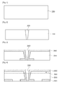
- FIGS. 1 to 5 are sectional views illustrating a method for manufacturing a solar cell according to the present invention.
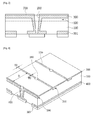
- FIG. 6 is a partial sectional view illustrating a solar cell manufactured through the method for manufacturing a solar cell according to the present invention.
- FIG. 7 is a top view illustrating a solar cell having a general fine line finger.
- FIG. 8 is a top view illustrating a solar cell having a fine line finger according to the present invention.
- via holes 200 are formed in a wafer 100.
- the via holes 2 are formed so as to pass through the front surface and the rear surface of a prepared silicon wafer 100 using a laser.
- the diameter of the via holes 200 may become gradually smaller as it goes from the front surface to the rear surface of the wafer 100.
- the wafer 100 having the via holes 200 is etched and cleaned.
- the etching step includes alkali etching or acid etching and the front surface of the wafer 100 is textured to improve absorption.
- first n-type contact holes contacting the via holes 200 are formed on the rear surface of the wafer 100.
- a shallow emitter 300 is formed on the inner walls of the via holes 200 and the front surface and the rear surface of the wafer 100 linking the via holes 200.
- the shallow emitter 300 with a low density is formed on the front surface of the wafer 100, the rear surface of the wafer 100, and the inner walls of the via holes 200.
- the reference numeral '301' designates a shallow emitter layer in FIGS. 4 and 6 .
- an emitter doping layer is compensated by aluminum (Al) to be converted into a p-type doping layer in the process of printing and heat-treating Al.
- the compensation is a process of doping Al (a p-type dopant) with a concentration higher than that of an emitter (of an n-type) to convert the emitter doping layer into a p-type doping layer.
- a selective emitter 500 is formed in a plurality of regions of the shallow emitter 300 along a direction of linking the via holes 200 by heavily doping a dopant so as to have a certain density or higher.
- the heavy doping of the present invention may follow one of two methods, i.e. a laser doping method and an etch back method.
- phosphorus silicate glass may be formed on the front surface of the wafer 100 by heavy doping and may be annealed using a laser to form the selective emitter 500.
- the location of the selective emitter 50 with a high density is a region where an electrode or the following fine line finger 700 is provided.
- PSG with a high density may be formed on the front surface of the wafer 100 by heavy doping and a plurality of regions along a direction linking the via holes 200 may be masked to form the selective emitter 500 after external portions of the masked regions are etched back.
- an alternative method is a doping paste method.
- doping paste containing phosphorus (P) is coated on the wafer 100 and the P contained in the doping paste is doped by heat treatment at a high temperature to form a heavy emitter.
- the selective emitter 500 is formed by performing a shallow emitter process.
- the coating of the paste is performed by screen printing, ink-jet printing, etc. It is preferable that a tube type furnace is used in a heat treating process at a high temperature and heavy doping and shallow doping are sequentially performed in a single process.
- the etchant may include an aqueous HF chemical etchant, an HF dry etchant, or a plasma etchant.
- a silicon nitride layer is deposited on the front surface of the wafer 100 to form a reflection preventing coating.
- the silicon nitride layer is deposited by plasma chemical vapor deposition (PCVD).
- silver (Ag) is printed on the front surface of the wafer 100 and Al is printed on the rear surface of the wafer 100.
- a solar cell test process is performed.
- the shallow emitter 300 is formed first, and after the selective emitter 500 is formed by heavy doping, the PSG left due to diffusion is removed. Then, the silicon nitride layer is deposited on the front and rear surfaces of the wafer 100 using chemical vapor deposition (CVD) and Al is printed on the rear surface of the wafer 100.
- CVD chemical vapor deposition
- the fine line finger 700 is formed so as to be connected to the via holes 200 along a direction of linking the via holes 200.
- Plating is performed during a metal forming process to perform a solar cell test process.
- the height H2, width W2, and the cross-sectional area of the fine line finger 700 are 9 ⁇ m, 60 ⁇ m, and 270 ⁇ m 2 respectively.
- the shading loss % is 2.6% for the fine line finger 700 according to the present invention and 5.2% for the general fine line finger 700.
- the distance between the fine line fingers is 2.3 mm.
Landscapes
- Photovoltaic Devices (AREA)
- Drying Of Semiconductors (AREA)
Applications Claiming Priority (2)
| Application Number | Priority Date | Filing Date | Title |
|---|---|---|---|
| KR1020090037050A KR101072543B1 (ko) | 2009-04-28 | 2009-04-28 | 태양 전지의 제조 방법 |
| PCT/KR2010/003028 WO2010126346A2 (fr) | 2009-04-28 | 2010-05-13 | Procédé de fabrication d'une cellule solaire |
Publications (2)
| Publication Number | Publication Date |
|---|---|
| EP2410574A2 true EP2410574A2 (fr) | 2012-01-25 |
| EP2410574A4 EP2410574A4 (fr) | 2015-08-19 |
Family
ID=43032720
Family Applications (1)
| Application Number | Title | Priority Date | Filing Date |
|---|---|---|---|
| EP10769991.0A Withdrawn EP2410574A4 (fr) | 2009-04-28 | 2010-05-13 | Procédé de fabrication d'une cellule solaire |
Country Status (5)
| Country | Link |
|---|---|
| US (1) | US20120270356A1 (fr) |
| EP (1) | EP2410574A4 (fr) |
| KR (1) | KR101072543B1 (fr) |
| CN (1) | CN102224601B (fr) |
| WO (1) | WO2010126346A2 (fr) |
Cited By (3)
| Publication number | Priority date | Publication date | Assignee | Title |
|---|---|---|---|---|
| US8916410B2 (en) | 2011-05-27 | 2014-12-23 | Csi Cells Co., Ltd | Methods of manufacturing light to current converter devices |
| US9153713B2 (en) | 2011-04-02 | 2015-10-06 | Csi Cells Co., Ltd | Solar cell modules and methods of manufacturing the same |
| US9660121B2 (en) | 2012-09-11 | 2017-05-23 | Rec Solar Pte. Ltd. | Method for fabricating a solar module of rear contact solar cells using linear ribbon-type connector strips and respective solar module |
Families Citing this family (6)
| Publication number | Priority date | Publication date | Assignee | Title |
|---|---|---|---|---|
| US20120122265A1 (en) * | 2010-11-17 | 2012-05-17 | Hitachi Chemical Company, Ltd. | Method for producing photovoltaic cell |
| CN102903786A (zh) * | 2011-07-29 | 2013-01-30 | 刘莹 | 一种新型超浅结晶体硅太阳能电池 |
| CN102683484B (zh) * | 2012-04-13 | 2015-05-13 | 苏州阿特斯阳光电力科技有限公司 | 背接触硅太阳能电池的制备方法 |
| CN102820343B (zh) * | 2012-08-16 | 2014-12-10 | 常州天合光能有限公司 | 具有无发射极区的太阳能电池及其制备方法 |
| WO2014179366A1 (fr) * | 2013-04-29 | 2014-11-06 | Soiexel, Inc. | Recuit pour traitement au laser ne générant pas de dommages pour des cellules solaires de haut rendement |
| US9716192B2 (en) | 2014-03-28 | 2017-07-25 | International Business Machines Corporation | Method for fabricating a photovoltaic device by uniform plating on emitter-lined through-wafer vias and interconnects |
Family Cites Families (14)
| Publication number | Priority date | Publication date | Assignee | Title |
|---|---|---|---|---|
| US5468652A (en) * | 1993-07-14 | 1995-11-21 | Sandia Corporation | Method of making a back contacted solar cell |
| JP3844552B2 (ja) * | 1997-02-26 | 2006-11-15 | 株式会社半導体エネルギー研究所 | 半導体装置の作製方法 |
| EP0881694A1 (fr) * | 1997-05-30 | 1998-12-02 | Interuniversitair Micro-Elektronica Centrum Vzw | Cellule solaire et méthode de fabrication |
| US6441297B1 (en) * | 1998-03-13 | 2002-08-27 | Steffen Keller | Solar cell arrangement |
| AUPP437598A0 (en) * | 1998-06-29 | 1998-07-23 | Unisearch Limited | A self aligning method for forming a selective emitter and metallization in a solar cell |
| US6524880B2 (en) * | 2001-04-23 | 2003-02-25 | Samsung Sdi Co., Ltd. | Solar cell and method for fabricating the same |
| US20050172996A1 (en) * | 2004-02-05 | 2005-08-11 | Advent Solar, Inc. | Contact fabrication of emitter wrap-through back contact silicon solar cells |
| US7144751B2 (en) * | 2004-02-05 | 2006-12-05 | Advent Solar, Inc. | Back-contact solar cells and methods for fabrication |
| US20060060238A1 (en) * | 2004-02-05 | 2006-03-23 | Advent Solar, Inc. | Process and fabrication methods for emitter wrap through back contact solar cells |
| KR20060007172A (ko) * | 2004-07-19 | 2006-01-24 | 매그나칩 반도체 유한회사 | 반도체 소자의 구리 금속배선 형성방법 |
| DE102006058267A1 (de) * | 2006-12-08 | 2008-06-12 | Q-Cells Ag | Emitter Wrap-Through-Solarzelle und Verfahren zur Herstellung einer Emitter Wrap-Through-Solarzelle |
| JP5285880B2 (ja) * | 2007-08-31 | 2013-09-11 | シャープ株式会社 | 光電変換素子、光電変換素子接続体および光電変換モジュール |
| JP5111063B2 (ja) * | 2007-11-12 | 2012-12-26 | シャープ株式会社 | 光電変換素子及びその製造方法 |
| US20090229665A1 (en) * | 2008-03-13 | 2009-09-17 | E. I. Du Pont De Nemours And Company | Aluminum pastes and use thereof in the production of silicon solar cells |
-
2009
- 2009-04-28 KR KR1020090037050A patent/KR101072543B1/ko not_active Expired - Fee Related
-
2010
- 2010-05-13 EP EP10769991.0A patent/EP2410574A4/fr not_active Withdrawn
- 2010-05-13 US US13/056,543 patent/US20120270356A1/en not_active Abandoned
- 2010-05-13 WO PCT/KR2010/003028 patent/WO2010126346A2/fr not_active Ceased
- 2010-05-13 CN CN2010800023412A patent/CN102224601B/zh not_active Expired - Fee Related
Non-Patent Citations (1)
| Title |
|---|
| See references of WO2010126346A2 * |
Cited By (8)
| Publication number | Priority date | Publication date | Assignee | Title |
|---|---|---|---|---|
| US9153713B2 (en) | 2011-04-02 | 2015-10-06 | Csi Cells Co., Ltd | Solar cell modules and methods of manufacturing the same |
| US8916410B2 (en) | 2011-05-27 | 2014-12-23 | Csi Cells Co., Ltd | Methods of manufacturing light to current converter devices |
| US9209342B2 (en) | 2011-05-27 | 2015-12-08 | Csi Cells Co., Ltd | Methods of manufacturing light to current converter devices |
| US9281435B2 (en) | 2011-05-27 | 2016-03-08 | Csi Cells Co., Ltd | Light to current converter devices and methods of manufacturing the same |
| US9660121B2 (en) | 2012-09-11 | 2017-05-23 | Rec Solar Pte. Ltd. | Method for fabricating a solar module of rear contact solar cells using linear ribbon-type connector strips and respective solar module |
| US10396227B2 (en) | 2012-09-11 | 2019-08-27 | Rec Solar Pte. Ltd. | Method for fabricating a solar module of rear contact solar cells using linear ribbon-type connector strips and respective solar module |
| US11183606B2 (en) | 2012-09-11 | 2021-11-23 | Rec Solar Pte. Ltd. | Method for fabricating a solar module of rear contact solar cells using linear ribbon-type connector strips and respective solar module |
| US11715806B2 (en) | 2012-09-11 | 2023-08-01 | Rec Solar Pte. Ltd. | Method for fabricating a solar module of rear contact solar cells using linear ribbon-type connector strips and respective solar module |
Also Published As
| Publication number | Publication date |
|---|---|
| EP2410574A4 (fr) | 2015-08-19 |
| WO2010126346A2 (fr) | 2010-11-04 |
| CN102224601A (zh) | 2011-10-19 |
| WO2010126346A4 (fr) | 2011-04-07 |
| KR20100118292A (ko) | 2010-11-05 |
| US20120270356A1 (en) | 2012-10-25 |
| CN102224601B (zh) | 2013-12-25 |
| WO2010126346A3 (fr) | 2011-02-17 |
| KR101072543B1 (ko) | 2011-10-11 |
Similar Documents
| Publication | Publication Date | Title |
|---|---|---|
| EP2410574A2 (fr) | Procédé de fabrication d'une cellule solaire | |
| EP2371010B1 (fr) | Cellule photovoltaïque, et procédé de fabrication correspondant | |
| US8569614B2 (en) | Solar cell and method of manufacturing the same | |
| KR101561682B1 (ko) | 깊은 홈 후측 콘택 광발전 태양 전지들 | |
| US8664015B2 (en) | Method of manufacturing photoelectric device | |
| US9087940B2 (en) | Photovoltaic solar cell and method for producing a photovoltaic solar cell | |
| KR101383395B1 (ko) | 후면전극형 태양전지의 제조방법 | |
| CN114050105A (zh) | 一种TopCon电池的制备方法 | |
| KR101159277B1 (ko) | 강유전체를 이용한 태양전지의 제조방법 | |
| KR101165915B1 (ko) | 태양전지의 제조방법 | |
| JP2013110406A (ja) | 光電変換素子の製造方法及び光電変換素子 | |
| JP5817046B2 (ja) | 背面接触式結晶シリコン太陽電池セルの製造方法 | |
| CN220290821U (zh) | 电池结构及太阳电池 | |
| JP2010080576A (ja) | 光電変換素子およびその製造方法 | |
| KR101370225B1 (ko) | 태양전지의 제조방법 및 그를 이용하여 제조된 태양전지 | |
| KR101198430B1 (ko) | 양면 수광형 국부화 에미터 태양전지 및 그 제조 방법 | |
| JP5645734B2 (ja) | 太陽電池素子 | |
| KR101181625B1 (ko) | 국부화 에미터 태양전지 및 그 제조 방법 | |
| TWI469367B (zh) | 背接觸式太陽能電池 | |
| KR101114198B1 (ko) | 국부화 에미터 태양전지 및 그 제조 방법 | |
| KR101251878B1 (ko) | 양면 수광형 태양전지 제조 방법 | |
| KR101382047B1 (ko) | 태양전지의 선택적 에미터 형성방법 | |
| KR101251857B1 (ko) | 양면 수광형 태양전지 제조 방법 | |
| KR101251856B1 (ko) | 양면 수광형 태양전지 제조 방법 | |
| KR101612132B1 (ko) | 후면전극형 태양전지의 제조방법 |
Legal Events
| Date | Code | Title | Description |
|---|---|---|---|
| PUAI | Public reference made under article 153(3) epc to a published international application that has entered the european phase |
Free format text: ORIGINAL CODE: 0009012 |
|
| 17P | Request for examination filed |
Effective date: 20110727 |
|
| AK | Designated contracting states |
Kind code of ref document: A2 Designated state(s): AL AT BE BG CH CY CZ DE DK EE ES FI FR GB GR HR HU IE IS IT LI LT LU LV MC MK MT NL NO PL PT RO SE SI SK SM TR |
|
| DAX | Request for extension of the european patent (deleted) | ||
| A4 | Supplementary search report drawn up and despatched |
Effective date: 20150720 |
|
| RIC1 | Information provided on ipc code assigned before grant |
Ipc: H01L 31/18 20060101AFI20150714BHEP |
|
| STAA | Information on the status of an ep patent application or granted ep patent |
Free format text: STATUS: THE APPLICATION IS DEEMED TO BE WITHDRAWN |
|
| 18D | Application deemed to be withdrawn |
Effective date: 20160217 |