EP2421135A2 - Convertisseur abaisseur, onduleur et procédé de fonctionnement - Google Patents
Convertisseur abaisseur, onduleur et procédé de fonctionnement Download PDFInfo
- Publication number
- EP2421135A2 EP2421135A2 EP11006639A EP11006639A EP2421135A2 EP 2421135 A2 EP2421135 A2 EP 2421135A2 EP 11006639 A EP11006639 A EP 11006639A EP 11006639 A EP11006639 A EP 11006639A EP 2421135 A2 EP2421135 A2 EP 2421135A2
- Authority
- EP
- European Patent Office
- Prior art keywords
- output
- circuit
- buck converter
- switch
- voltage
- Prior art date
- Legal status (The legal status is an assumption and is not a legal conclusion. Google has not performed a legal analysis and makes no representation as to the accuracy of the status listed.)
- Granted
Links
Images



Classifications
-
- H—ELECTRICITY
- H02—GENERATION; CONVERSION OR DISTRIBUTION OF ELECTRIC POWER
- H02M—APPARATUS FOR CONVERSION BETWEEN AC AND AC, BETWEEN AC AND DC, OR BETWEEN DC AND DC, AND FOR USE WITH MAINS OR SIMILAR POWER SUPPLY SYSTEMS; CONVERSION OF DC OR AC INPUT POWER INTO SURGE OUTPUT POWER; CONTROL OR REGULATION THEREOF
- H02M3/00—Conversion of DC power input into DC power output
- H02M3/02—Conversion of DC power input into DC power output without intermediate conversion into AC
- H02M3/04—Conversion of DC power input into DC power output without intermediate conversion into AC by static converters
- H02M3/10—Conversion of DC power input into DC power output without intermediate conversion into AC by static converters using discharge tubes with control electrode or semiconductor devices with control electrode
- H02M3/145—Conversion of DC power input into DC power output without intermediate conversion into AC by static converters using discharge tubes with control electrode or semiconductor devices with control electrode using devices of a triode or transistor type requiring continuous application of a control signal
- H02M3/155—Conversion of DC power input into DC power output without intermediate conversion into AC by static converters using discharge tubes with control electrode or semiconductor devices with control electrode using devices of a triode or transistor type requiring continuous application of a control signal using semiconductor devices only
- H02M3/156—Conversion of DC power input into DC power output without intermediate conversion into AC by static converters using discharge tubes with control electrode or semiconductor devices with control electrode using devices of a triode or transistor type requiring continuous application of a control signal using semiconductor devices only with automatic control of output voltage or current, e.g. switching regulators
- H02M3/158—Conversion of DC power input into DC power output without intermediate conversion into AC by static converters using discharge tubes with control electrode or semiconductor devices with control electrode using devices of a triode or transistor type requiring continuous application of a control signal using semiconductor devices only with automatic control of output voltage or current, e.g. switching regulators including plural semiconductor devices as final control devices for a single load
- H02M3/1584—Conversion of DC power input into DC power output without intermediate conversion into AC by static converters using discharge tubes with control electrode or semiconductor devices with control electrode using devices of a triode or transistor type requiring continuous application of a control signal using semiconductor devices only with automatic control of output voltage or current, e.g. switching regulators including plural semiconductor devices as final control devices for a single load with a plurality of power processing stages connected in parallel
-
- H—ELECTRICITY
- H02—GENERATION; CONVERSION OR DISTRIBUTION OF ELECTRIC POWER
- H02M—APPARATUS FOR CONVERSION BETWEEN AC AND AC, BETWEEN AC AND DC, OR BETWEEN DC AND DC, AND FOR USE WITH MAINS OR SIMILAR POWER SUPPLY SYSTEMS; CONVERSION OF DC OR AC INPUT POWER INTO SURGE OUTPUT POWER; CONTROL OR REGULATION THEREOF
- H02M7/00—Conversion of AC power input into DC power output; Conversion of DC power input into AC power output
- H02M7/42—Conversion of DC power input into AC power output without possibility of reversal
- H02M7/44—Conversion of DC power input into AC power output without possibility of reversal by static converters
- H02M7/48—Conversion of DC power input into AC power output without possibility of reversal by static converters using discharge tubes with control electrode or semiconductor devices with control electrode
- H02M7/53—Conversion of DC power input into AC power output without possibility of reversal by static converters using discharge tubes with control electrode or semiconductor devices with control electrode using devices of a triode or transistor type requiring continuous application of a control signal
- H02M7/537—Conversion of DC power input into AC power output without possibility of reversal by static converters using discharge tubes with control electrode or semiconductor devices with control electrode using devices of a triode or transistor type requiring continuous application of a control signal using semiconductor devices only, e.g. single switched pulse inverters
- H02M7/5387—Conversion of DC power input into AC power output without possibility of reversal by static converters using discharge tubes with control electrode or semiconductor devices with control electrode using devices of a triode or transistor type requiring continuous application of a control signal using semiconductor devices only, e.g. single switched pulse inverters in a bridge configuration
- H02M7/53871—Conversion of DC power input into AC power output without possibility of reversal by static converters using discharge tubes with control electrode or semiconductor devices with control electrode using devices of a triode or transistor type requiring continuous application of a control signal using semiconductor devices only, e.g. single switched pulse inverters in a bridge configuration with automatic control of output voltage or current
-
- H—ELECTRICITY
- H02—GENERATION; CONVERSION OR DISTRIBUTION OF ELECTRIC POWER
- H02M—APPARATUS FOR CONVERSION BETWEEN AC AND AC, BETWEEN AC AND DC, OR BETWEEN DC AND DC, AND FOR USE WITH MAINS OR SIMILAR POWER SUPPLY SYSTEMS; CONVERSION OF DC OR AC INPUT POWER INTO SURGE OUTPUT POWER; CONTROL OR REGULATION THEREOF
- H02M1/00—Details of apparatus for conversion
- H02M1/0067—Converter structures employing plural converter units, other than for parallel operation of the units on a single load
- H02M1/007—Plural converter units in cascade
-
- H—ELECTRICITY
- H02—GENERATION; CONVERSION OR DISTRIBUTION OF ELECTRIC POWER
- H02M—APPARATUS FOR CONVERSION BETWEEN AC AND AC, BETWEEN AC AND DC, OR BETWEEN DC AND DC, AND FOR USE WITH MAINS OR SIMILAR POWER SUPPLY SYSTEMS; CONVERSION OF DC OR AC INPUT POWER INTO SURGE OUTPUT POWER; CONTROL OR REGULATION THEREOF
- H02M1/00—Details of apparatus for conversion
- H02M1/0067—Converter structures employing plural converter units, other than for parallel operation of the units on a single load
- H02M1/0074—Plural converter units whose inputs are connected in series
-
- H—ELECTRICITY
- H02—GENERATION; CONVERSION OR DISTRIBUTION OF ELECTRIC POWER
- H02M—APPARATUS FOR CONVERSION BETWEEN AC AND AC, BETWEEN AC AND DC, OR BETWEEN DC AND DC, AND FOR USE WITH MAINS OR SIMILAR POWER SUPPLY SYSTEMS; CONVERSION OF DC OR AC INPUT POWER INTO SURGE OUTPUT POWER; CONTROL OR REGULATION THEREOF
- H02M1/00—Details of apparatus for conversion
- H02M1/0067—Converter structures employing plural converter units, other than for parallel operation of the units on a single load
- H02M1/0077—Plural converter units whose outputs are connected in series
Definitions
- the invention relates to a buck converter circuit having two parallel main branches between an input and an output side, an input side capacitor series circuit between the main branches, a diode series circuit between the main branches, a middle branch connecting an intermediate node of the input side capacitor series circuit with an intermediate node of the diode series circuit, depending on a storage inductor in the two main branches between the diode series circuit and the output side, one clocked controllable switch in the two main branches between the input side capacitor series circuit and the diode series circuit and a control unit for driving the switch in a switch driving mode, in which they the two switches at different times and / or switched to different switching positions, and to a transformerless inverter circuit arrangement equipped therewith, as used, for example, for grid connection of photovoltaic systems, small wind generators and general DC power sources, as well as to associated operating methods.
- a buck converter circuit and an inverter circuit arrangement of this kind are disclosed in the publication DE 10 2005 047 373 A1 disclosed. Compared with other conventional circuits of this type mentioned there, the circuits disclosed therein can be implemented with comparatively little effort and volume and with low EMC problems, and permit operation with comparatively high efficiency.
- the invention is based on the technical problem of providing a buck converter circuit and a transformerless inverter circuit arrangement of the type mentioned above and associated operating methods, which can be implemented with relatively little effort and volume and low EMC problems, have high efficiency and specific functionality , as it is particularly advantageous for grid connection of DC power sources, such as photovoltaic systems and fuel cell systems.
- the invention solves this problem by providing a buck converter circuit having the features of claim 1, a transformerless inverter circuit arrangement with the features of claim 9, a method for operating such a buck converter circuit with the features of claim 14 and a method for operating such an inverter circuit arrangement with the features of claim 15.
- the buck converter circuit according to the invention is based on the buck converter circuit of DE 10 2005 047 373 A1 and in so far has the advantages described there compared to other conventional buck converter circuits, in particular when used in a transformerless inverter circuit arrangement.
- the buck converter circuit according to the invention has an output-side capacitor series circuit between the two main branches and the central branch is continued up to an intermediate node of this output-side capacitor bank circuit. This circuit structure allows a very advantageous operation of the buck converter circuit with further improved efficiency.
- the arrangement of at least one diode, which is in each case connected in parallel to one of the capacitors of the output-side capacitor series circuit, is advantageous. This prevents the voltage at the respective capacitor from becoming negative in corresponding switch drive modes, i. is reversed.
- the output side capacitor series circuit has between the two capacitors an intermediate node which is connected to the central branch of the buck converter circuit. At this intermediate node is then for example (potential equal) connected to one and / or both of the capacitors each have a diode in parallel, wherein in the arrangement of a respective diode to the capacitors, provided between the diodes intermediate node is also connected to the central branch.
- the alternative arrangement of the second diode is shown in the drawing, in particular in Fig. 1 and 6 indicated by dashed lines.
- the current flow directions of the diodes which are each connected in parallel to one of the capacitors of the output-side capacitor series circuit, are each antisymmetric with respect to the central branch, that is to say a first diode is connected between central branch and one of the main branches external, blocking the other main branch.
- the arrangement of the diode (s) on the capacitor (s) of the output side capacitor bank is parallel to the diode series connection of the at least two serially connected diodes between the two main branches connected between the upstream and the downstream capacitor banks is arranged.
- the control unit is set up to control the clocked activatable switch of the buck converter circuit in four different drive modes, depending on whether an output voltage based on an input voltage amount above or below a predetermined threshold and whether it is in each case a first or second half-wave of the output voltage.
- the thus formed further buck converter circuit is particularly suitable for carrying out the buck converter circuit operating method according to the invention. It can thus be produced in a very good approximation sinusoidal output voltage half-oscillations with comparatively little effort and increased efficiency with minimal EMC problems. This can be used in particular for a correspondingly advantageous operation of the inverter circuit arrangement according to the invention, which is equipped with the step-down converter circuit according to the invention.
- the step-down converter constructed from two symmetrical halves jointly generates a single output voltage.
- the proposed structure a division of the voltage stress of the components is achieved.
- the buck converter built up from two symmetrical halves is fed from a single input voltage. Also by this variant, a reduction of the voltage stress of the components is achieved in an advantageous manner.
- the pulsating DC voltage at the output of the buck converter has the form of a sine half wave, since the output side of the buck converter circuit, in particular in the application example of an inverter circuit, a sinusoidal voltage waveform to be realized.
- a pulsating DC voltage is formed at the output of the step-down converter or the DC voltage at the output of the step-down converter pulses at a frequency of 100 Hz or 120 Hz.
- the said repetition time or pulsation frequency is adjusted to the output (mains) frequency and is either half the period or twice the (mains) frequency.
- the two halves of the symmetrically constructed buck converter are controlled such that voltages on the capacitors of the input-side capacitor series circuit assume the same value or the two halves of the symmetrically configured buck converter are controlled such that the voltages across the capacitors the input-side capacitor series circuit remain in a certain ratio or stand.
- the symmetrical structure of the buck converter refers to the middle branch.
- the two halves of the symmetrically constructed buck converter be controlled so that they each remove the same amount of charge from the capacitors of the input-side capacitor series circuit.
- the control is preferably carried out in such a way that in each case the same voltage is applied after each half-wave to the capacitors of the input-side capacitor series circuit. This results in a lower voltage load for these capacitors and therefore there is basically the possibility to use here few expensive - and therefore also cheap - components.
- both switches are clocked in the two main branches at times.
- the inverter circuit arrangement is designed for coupling to a three-phase network.
- the inverter circuit arrangement implements a switched T-filter with which the ripple of the current profile can be reduced on the output side.
- one or more attenuation elements are provided at corresponding points of the inverter circuit arrangement, which are dimensioned for damping resonance points of the T-filter structure.
- an energy-dissipating component for example, a resistor or a series connection of a capacitance and an inductance, optionally together with a resistor, are considered as examples.
- the arrangement is here in particular chosen such that the natural oscillating behavior at the lowest resonant frequency is compensated by the control unit of the buck converter circuit.
- the additional, advantageously provided at different locations attenuators cause the higher-frequency natural oscillations of these components or assemblies are attenuated, thereby improving the electromagnetic compatibility on the one hand, but possibly also the efficiency on the other hand.
- Inverter circuitry shown is of a dynamic intermediate circuit type comprising a buck converter circuit 10 and a pole inverter / inverter bridge circuit 11 coupled thereto.
- the inverter circuit arrangement can be used, for example, for grid connection of a photovoltaic DC voltage generator G, as in Fig. 1 shown as an example and representative of numerous other applications.
- the buck converter circuit 10 includes two main branches 1, 2 each between an input terminal E1, E2 and an output terminal A1, A2, in each of which a controllable switch S1 S2 and an inductance or storage inductor L1, L2 are located in series.
- the side of the buck converter circuit 10 facing the DC voltage generator G is referred to as the input side and the other side as the output side.
- a diode series circuit is shown in FIG Example, two diodes D1, D2 looped, wherein the node of the diode series circuit D1, D2 with the respective main branch 1, 2 between the respective switch S1 S2 and the respective storage inductor L1, L2 is located.
- the buck converter circuit 10 has a middle branch 3 connecting an intermediate node KCE of the input-side capacitor series circuit C1, C2 to an intermediate node KD of the diode series circuit D1, D2 and an intermediate node KCA of the output-side capacitor series circuit C3, C4, otherwise no further connection to the input side and to the output side of the buck converter circuit, in particular no further connection to one of the main branches 1, 2.
- the middle branch 3 is a fixed connection, but in alternative embodiments it may also be a switchable connection or in general an impedance (For example, inductance and / or capacitance and / or resistance) be realized.
- the inverter circuit arrangement of Fig. 1 with the buck converter circuit 10 for example, for grid coupling of a photovoltaic generator or fuel cells.
- the input-side voltage source may, for example, also be the output circuit of a boost converter, as in the case of the application for network coupling of smaller fuel cell systems.
- the buck converter circuit 10 supplies the output side, a voltage U B , which is also the input voltage of the coupled Polwender- / inverter bridge circuit 11, again for ease of orientation (without limitation, the application hereon) the buck converter circuit 10 side facing the Polwender- / inverter bridge circuit 11th as their input side and their power grid 5 facing side are referred to as the output side.
- respective capacitor voltages U C1 , U C2 , U C3 , U C4 are applied to the four capacitors C1 to C4 of the buck converter circuit.
- the input-side current intensity is denoted by I G , the main branch currents flowing through the storage chokes L1, L2 with I L1 or I L2 and the output-side current intensity with I B.
- the switches S1, S2 are driven by associated clock control signals T S1 , T S2 .
- the Polwender- / inverter bridge circuit 11 comprises in a conventional manner a Polwender- / full bridge part with four controllable Polwender- / full bridge switches S3, S4, S5, S6, at the two Brückenabgriffe each an inductance L3, L4 is coupled to the input side of a corresponding Bridge tap voltage U BW is applied and the output side provide the output voltage U w .
- a feed-in current I w can thereby be supplied, wherein symbolically an associated network impedance Z w of the public power grid 5 in FIG Fig. 1 is specified.
- the control or regulation of the inverter circuit arrangement is preferably carried out in the form of a state control, ie in the form of a control on the energy-carrying variables, such as inductor currents and capacitor voltages.
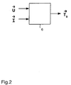
- This state control is in an in Fig. 2 implemented schematically shown control unit 6.
- the relevant voltage information in Fig. 2 shown summarily with a voltage vector U, and amperage information supplied in Fig. 2 symbolic represented with a current vector I.
- the voltage vector U includes as components in particular the buck converter input voltage U E , the capacitor voltages U C1 to U C4 , the bridge voltage U B , the full-bridge output voltage U BW and the output voltage U w of Polwender- / AC bridge circuit 11. Since the sum U C1 + U C2 of the two input-side capacitor voltages U C1, U C2 is equal to the input voltage U E, it is sufficient, in alternative embodiments, the control unit 6, only two of the three voltage information U E , U C1 , U C2 supply.
- the control unit 6 only needs two of the three voltage information U B , U input voltage U E , the capacitor voltages U C1 to U C4 , the bridge voltage U B , the full-bridge output voltage U BW and the output voltage U w of the polarizer Since the sum U C1 + U C2 of the two input side capacitor voltages U C1 , U C2 is equal to the input voltage U E , it suffices in alternative embodiments, the control unit 6 only two of the three voltage information U E , U C1 , U C2 supply.
- the control unit 6 it is sufficient for the control unit 6 to supply only two of the three voltage information U B , U C3 , U C4 , since the sum U C3 + U C4 of the two output-side capacitor voltages U C3 , U C4 is equal to the bridge voltage U B.
- the current vector I includes as components in particular the input current intensity I G , the buck converter inductor currents I L1 , I L2 , the full-bridge input current or bridge current I B and the output current I w of the pole inverter inverter bridge circuit 11.
- one or more the state variables not obtained by measurement, but generated by a corresponding so-called route observer. This is particularly useful for state variables that are difficult to measure.
- the control unit 6 acquires the output information or control signals required for the state control of the system, in particular the drive clock signals T S1 , T S2 for the two buck converter switches S1 S2 and drive clock signals T S3 , T S4 , T S5 , T S6 for the four full bridge switches S3 to S6.
- the drive clock signals T S1 , T S2 for the two buck converter switches S1 S2
- drive clock signals T S3 , T S4 , T S5 , T S6 for the four full bridge switches S3 to S6.
- the control unit 6 is of a customary for the application mentioned, familiar to those skilled construction, which therefore requires no further explanation here.
- the control unit 6 For controlling the two buck converter switches S1, S2, the control unit 6 uses as input information in particular the bridge voltage U B , the input voltage U E and the capacitor voltages U C1 to U C4 . On the basis of this input information, it outputs the drive clock signals T S1 , T S2 for the two switches S1, S2.
- a favorable design and control strategy for the buck converter circuit 10 is to keep the changes in the bridge voltage U B during the clock switching operations of the switches S1, S2 as small as possible, since this keeps the current changes in the inductors L1, L2 correspondingly low. This contributes in addition to a favorable, subsequently in connection with the Fig.
- two capacitors C1, C2 or C3, C4 of the same capacitance are respectively selected for the input-side and / or the output-side capacitor series circuit, so that half of the input voltage U E is present, for example, at the input-side intermediate node KCE.
- capacitors of different capacitance or more than two capacitors for the respective capacitor series circuit are possible, and analogously, more than two diodes for the diode series connection are possible in alternative embodiments.
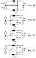
- the Fig. 3A to 3D illustrate in schematic, simplified circuit diagrams the operation and the operation of the buck converter circuit 10 of Fig. 1 for the four possible different positions of the two clock switches S1 S2 for the one, eg positive current flow direction.
- state A the two switches S1, S2 are closed.
- the two diodes D1, D2 block, ie the diode series circuit D1, D2 does not form an active current path and is therefore in Fig. 3A not shown.
- a between the main branches 1, 2 at the level before the two chokes L1, L2 pending voltage U D also referred to herein as an intermediate circuit voltage is therefore equal to the input voltage U E.
- both switches S1, S2 are opened or interrupted, whereby the two diodes D1, D2 are conductive. This means that the intermediate circuit voltage U D practically assumes the value zero.
- state C the first switch S1 is opened or interrupted, while the second switch S2 is closed or conductive.
- the diode D2 connected between the central branch 3 and the closed switch S2 blocks, while the other diode D1 conducts.
- a DC link current path is formed, in which the capacitor C2 located between the central branch 3 and the closed switch S2 is located that the intermediate circuit voltage U D is equal to the voltage U C2 across this capacitor C2 and thus equal to a corresponding fraction of the input voltage U E.
- state D mirror image of the state C
- the first switch S1 is closed or conductive, while the second switch S2 is opened or locked. Accordingly, the diode D1 between the closed first switch S1 and the central branch 3, while the other diode D2 conducts, so that in turn forms over the central branch 3, a DC link current path, in which in this case between the closed switch S1 and the central branch 3 lying capacitor C1 is located.
- the intermediate circuit voltage U D consequently assumes the value of the voltage U C1 across this capacitor C1.
- the buck converter circuit 10 can be controlled by the control unit 6 by suitably clocked alternation between the four switching / operating states A, B, C, D of Fig. 3A to 3D be operated in different drive modes.
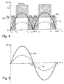
- the 4 and 5 illustrate a practical application for the mentioned grid connection of the photovoltaic generator G according to Fig. 1 , In this case, the mode of operation for two consecutive half-cycles of the bridge voltage U B or the output voltage U W of the inverter circuit arrangement is shown in the time diagram.
- the clocking sequence for the two switches S1, S2 is selected depending on whether the instantaneous value of the bridge voltage U B amount above or below a predetermined threshold U S , in the example shown, the half input voltage U E / 2 is selected as an example ,
- This threshold value U S corresponds to the voltage value that the DC link voltage assumes U D in the operating states C and D.
- the two switches S1, S2 are clocked in an initial interval [t 0 , t 1 ] of the first bridge voltage half-cycle by the control unit 6 with the cyclically repeated state sequence CBCB, ie it starts with the corresponding clock frequency between the state C of Fig.
- the control unit 6 changes to a second switch activation mode with the cyclically repeated state sequence ACAC, ie the switches S1, S2 are controlled so that repeated from state A of Fig. 3A to state C of Fig. 3C and switched back again. Specifically, this means that in the second drive mode, the switch S2 is kept closed, while the switch S1 is opened and closed in a clocked manner.
- the control unit 6 returns to the first activation mode for a final interval [t 2 , t 3 ] of the first bridge voltage half cycle, ie until the bridge voltage instantaneous value at the instant t 3 half the period T / 2 is back to zero.
- the control unit 6 then activates the two switches S1, S2 in a third activation mode with the cyclically repeated state sequence DBDB for an initial interval [t 3 , t 4 ] of the second bridge voltage half oscillation. This means, that the switch S2 is kept open and the switch S1 is opened and closed in a clocked manner.
- control unit 6 selects a fourth switch activation mode with the cyclically repeated state sequence ADAD for a corresponding mean interval [t 4 , t 5 ] of the second bridge voltage half-oscillation That is, in this fourth drive mode, the switch S1 is kept closed while the switch S2 is opened and closed in a clocked manner.
- Fig. 5 shows the supplied by the Polwender- / Wegnscrien 11 from the input side bridge voltage U B and the input side bridge current I B output voltage U W and the associated output current I W , said electrical output variables by folding the polarity of the second half-waves of the bridge voltage U B and the bridge current I B are generated.
- the full bridge / pole changeover switches S3 to S6 are switched diagonally for this purpose, ie the switches S3 and S6 are switched synchronously and in phase opposition to the switches S4, S5, which are also clocked synchronously with one another.
- the construction volume of the magnetic components, in particular of the storage chokes L1 and L2 can be significantly reduced, for example by a factor of about ten to about twenty. It also shows that the structure and operation of the inverter circuit of Fig. 1 and in particular of their buck converter circuit 10 allow a relatively high efficiency and cause only relatively low EMC problems.
- the inverter circuitry of Fig. 1 is referred to as a switched-T type filter, also known as an LCL filter, which is known to reduce the ripple in the current waveform to the output side of the circuitry.
- a switched-T type filter also known as an LCL filter
- This purpose is served, for example, by the output-side inductors L3, L4.
- the filter characteristics of the circuit arrangement are improved, which in turn favors the use of clock switches with reduced, eg halved, withstand voltage of, for example, only about 600V.
- Fig. 6 shows a variant of the circuit arrangement of Fig. 1 , which differs from this only in that additional attenuators DN1 to DN9 are provided at selected points of the circuit structure.
- a first attenuator DN1 of the inductor L1 is connected in parallel
- a second attenuator DN2 is connected in parallel to the inductor L2
- one attenuator DN3, DN4 is connected in parallel to the capacitors C3, C4
- an attenuator DN5 is connected to the output side of the buck converter circuit 10 between them
- Main branches 1, 2 looped an attenuator DN6 is looped between the inputs of the output side inductors L3, L4, one attenuator DN7, DN8 is connected in parallel to these inductors L3, L4 and an attenuator DN9 is connected between the outputs of these inductors L3, L4.
- Each of these attenuators DN1 to DN9 may be implemented by any conventional passive attenuation network using inductors, capacitors, linear and / or non-linear resistors.
- the attenuators DN1 to DN9 serve to dampen resonance points of the T-filter structure of the inverter circuit arrangement. This supports the resonance suppression, which incidentally by the implemented in the control unit 6 state control of the system and in particular for the feed current I w causes becomes.
- the attenuators DN1 to DN9 can supplement the resonance-damping contribution of the state control appropriately in the required manner, if the control-technical treatment of the resonance points alone does not appear to be sufficient due to active regulation in the context of state control, for example because of the generally variable network impedance z w .
- Attenuators DN3, DN4 and DN5 are used in alternative embodiments.
- the use of some attenuators DN3, DN4 and DN5 is to be emphasized, since with these already with great effectiveness in the suppression of unwanted vibrations is achieved.
- the attenuators DN3, DN4 which are arranged parallel to the capacitors C3, C4 of the output-side capacitor series circuit, ie represent a connection of the central branch 3 to the respective main branches 1, 2 in the region of the capacitors C3, C4 of the output-side capacitor series circuit.
- the inverter circuit arrangement according to the invention can be operated with reactive power if required, ie, by shifting the centroid of the sinusoidal waveform of the current to be injected, a reactive current component can be generated, possibly accompanied by a slight increase in the distortion current component or harmonic distortion factor ,
- the FIGS. 7 and 8 illustrate corresponding operating variants in the current / time diagram.
- I w ideal sinusoidal feed current
- FIGS. 7 and 8 illustrate corresponding operating variants in the current / time diagram.
- the two diagrams of the ideal sinusoidal feed current I w as he also in the diagram of Fig. 5 is shown, shown in dashed lines for the blind power-free operating case in which only active power is generated.
- Fig. 7 1 shows a feed-in current I W1 as output current of the polarity reversal / reversing bridge circuit for an operating variant in which a feed-in current I W1 with leading capacitive reactive current component is provided by advancing the centroid of the current sinusoid.
- Analog shows Fig. 8 the characteristic of a feed current I W2 with a lagging, inductive reactive current component. This feed-in current I W2 is generated by retarding the center of gravity of the current sinusoid.
- Both feed-in variants I W1 , I W2 with leading, capacitive reactive current component or lagging, inductive reactive current component can by appropriate operation of the inverter circuit arrangement according to the invention, for example with the in Fig. 1 or 6 shown topology can be realized, in particular by appropriate control of the switches S1 to S6.
- the invention provides a buck converter circuit which can be operated in a very advantageous manner and with a comparatively high degree of efficiency, which in particular can be even higher than that in the US Pat DE 10 2005 047 373 A1 disclosed buck converter circuit is achievable.
- the advantages and functional properties mentioned there apply in the same way to the present circuit arrangement insofar as they correspond in their circuit construction and their mode of operation.
- the increased efficiency can be achieved in particular by the special control of the buck converter switch, as above Fig. 4 in turn explained by the additional arrangement of the output-side capacitor series circuit and the connection of the central branch to this output-side capacitor series circuit is possible.
- the increased efficiency is also due to the at least one diode which is connected in parallel to one of the capacitors of the output-side capacitor series circuit.
- the use of these diodes is an improvement in the efficiency of about 0.2% absolute attributable.
- Next contributes to increased efficiency, a comparatively small mean voltage / time surface on the chokes L1, L2 at. This, in conjunction with the choice of suitable reactor core materials, allows an optimized design in terms of core and winding losses.
- the proposal according to the invention significantly increased the efficiencies of about 97% (state of the art prior to invention) which are typical for the inverter circuit arrangements in question.
- the embodiment of the invention reaches a peak of up to 99%! That is, the proportion of heat loss, which may need to be cooled with expensive measures, reduced by two thirds with the invention!
Landscapes
- Engineering & Computer Science (AREA)
- Power Engineering (AREA)
- Dc-Dc Converters (AREA)
Priority Applications (1)
| Application Number | Priority Date | Filing Date | Title |
|---|---|---|---|
| PL11006639T PL2421135T3 (pl) | 2010-08-20 | 2011-08-12 | Niezawierający transformatora układ połączeń falownika z układem połączeń przekształtnika zmniejszającego napięcie |
Applications Claiming Priority (1)
| Application Number | Priority Date | Filing Date | Title |
|---|---|---|---|
| DE102010035020A DE102010035020A1 (de) | 2010-08-20 | 2010-08-20 | Tiefsetzstellerschaltung, Wechselrichter-Schaltungsanordnung und Betriebsverfahren |
Publications (3)
| Publication Number | Publication Date |
|---|---|
| EP2421135A2 true EP2421135A2 (fr) | 2012-02-22 |
| EP2421135A3 EP2421135A3 (fr) | 2016-12-28 |
| EP2421135B1 EP2421135B1 (fr) | 2019-10-02 |
Family
ID=45092532
Family Applications (1)
| Application Number | Title | Priority Date | Filing Date |
|---|---|---|---|
| EP11006639.6A Active EP2421135B1 (fr) | 2010-08-20 | 2011-08-12 | Onduleur sans transformateur avec convertisseur abaisseur |
Country Status (4)
| Country | Link |
|---|---|
| EP (1) | EP2421135B1 (fr) |
| DE (1) | DE102010035020A1 (fr) |
| DK (1) | DK2421135T3 (fr) |
| PL (1) | PL2421135T3 (fr) |
Cited By (5)
| Publication number | Priority date | Publication date | Assignee | Title |
|---|---|---|---|---|
| CN103607128A (zh) * | 2013-12-06 | 2014-02-26 | 阳光电源股份有限公司 | 一种电压源型逆变器的控制方法及控制装置 |
| WO2013173160A3 (fr) * | 2012-05-15 | 2014-06-19 | General Electric Company | Convertisseur de puissance en mode commuté pour applications haute tension |
| EP2768130A1 (fr) * | 2013-02-19 | 2014-08-20 | Siemens Aktiengesellschaft | Convertisseur de tension continue |
| EP2852044A2 (fr) | 2013-09-23 | 2015-03-25 | SMA Solar Technology AG | Convertisseur bidirectionnel à direction préférentielle et onduleur capable de produire de la puissance reactive |
| CN114424443A (zh) * | 2019-09-18 | 2022-04-29 | 西门子股份公司 | 可灵活设计的转换器单元 |
Families Citing this family (2)
| Publication number | Priority date | Publication date | Assignee | Title |
|---|---|---|---|---|
| DE102014102000B3 (de) * | 2014-02-18 | 2014-09-11 | Sma Solar Technology Ag | Verfahren zum Betreiben eines blindleistungsfähigen Wechselrichters mit Polwender und blindleistungsfähiger Wechselrichter mit Polwender |
| DE102014203157A1 (de) * | 2014-02-21 | 2015-08-27 | Airbus Operations Gmbh | Bipolares Hochspannungsnetz und Verfahren zum Betreiben eines bipolaren Hochspannungsnetzes |
Citations (1)
| Publication number | Priority date | Publication date | Assignee | Title |
|---|---|---|---|---|
| DE102005047373A1 (de) | 2005-09-28 | 2007-04-05 | Schekulin, Dirk, Dr. Ing. | Tiefsetzstellerschaltung und Wechselrichter-Schaltungsanordnung |
Family Cites Families (6)
| Publication number | Priority date | Publication date | Assignee | Title |
|---|---|---|---|---|
| DE19700100C2 (de) * | 1997-01-03 | 2000-05-25 | Peter Moosbauer | Tiefsetzsteller |
| US5932995A (en) * | 1998-03-03 | 1999-08-03 | Magnetek, Inc. | Dual buck converter with coupled inductors |
| DE10360549A1 (de) * | 2003-12-22 | 2005-07-14 | Siemens Ag | Ausgangsfilter eines Mehrpunkt-Wechselrichters |
| JP4597626B2 (ja) * | 2004-03-01 | 2010-12-15 | 株式会社ダイヘン | アーク加工用電源装置及びインバータ電源装置 |
| DE102006014780A1 (de) * | 2006-03-29 | 2007-10-18 | Schekulin, Ulrich | Gleichstromsteller und Wechselrichter-Schaltungsanordnung |
| US8106540B2 (en) * | 2008-10-10 | 2012-01-31 | General Electric Company | Compensation system for power transmission |
-
2010
- 2010-08-20 DE DE102010035020A patent/DE102010035020A1/de not_active Withdrawn
-
2011
- 2011-08-12 DK DK11006639.6T patent/DK2421135T3/da active
- 2011-08-12 PL PL11006639T patent/PL2421135T3/pl unknown
- 2011-08-12 EP EP11006639.6A patent/EP2421135B1/fr active Active
Patent Citations (1)
| Publication number | Priority date | Publication date | Assignee | Title |
|---|---|---|---|---|
| DE102005047373A1 (de) | 2005-09-28 | 2007-04-05 | Schekulin, Dirk, Dr. Ing. | Tiefsetzstellerschaltung und Wechselrichter-Schaltungsanordnung |
Cited By (8)
| Publication number | Priority date | Publication date | Assignee | Title |
|---|---|---|---|---|
| WO2013173160A3 (fr) * | 2012-05-15 | 2014-06-19 | General Electric Company | Convertisseur de puissance en mode commuté pour applications haute tension |
| EP2768130A1 (fr) * | 2013-02-19 | 2014-08-20 | Siemens Aktiengesellschaft | Convertisseur de tension continue |
| EP2852044A2 (fr) | 2013-09-23 | 2015-03-25 | SMA Solar Technology AG | Convertisseur bidirectionnel à direction préférentielle et onduleur capable de produire de la puissance reactive |
| DE102014113306A1 (de) | 2013-09-23 | 2015-03-26 | Sma Solar Technology Ag | Bidirektionaler Wandler mit Vorzugsrichtung und blindleistungsfähige Wechselrichter mit diesem Wandler |
| US9300209B2 (en) | 2013-09-23 | 2016-03-29 | Sma Solar Technology Ag | Bidirectional converter with preferential direction and reactive power-capable inverter having said converter |
| CN103607128A (zh) * | 2013-12-06 | 2014-02-26 | 阳光电源股份有限公司 | 一种电压源型逆变器的控制方法及控制装置 |
| CN103607128B (zh) * | 2013-12-06 | 2016-03-30 | 阳光电源股份有限公司 | 一种电压源型逆变器的控制方法及控制装置 |
| CN114424443A (zh) * | 2019-09-18 | 2022-04-29 | 西门子股份公司 | 可灵活设计的转换器单元 |
Also Published As
| Publication number | Publication date |
|---|---|
| DK2421135T3 (da) | 2020-01-20 |
| EP2421135A3 (fr) | 2016-12-28 |
| EP2421135B1 (fr) | 2019-10-02 |
| DE102010035020A1 (de) | 2012-02-23 |
| PL2421135T3 (pl) | 2021-07-19 |
Similar Documents
| Publication | Publication Date | Title |
|---|---|---|
| EP1369985B1 (fr) | Onduleur pour transformer une tension continue en courant alternatif ou en tension alternative | |
| EP2391522B1 (fr) | Convertisseur cc/cc et convertisseur ca/cc | |
| EP2815497B1 (fr) | Dispositif d'alimentation réseau, système d'alimentation en énergie et procédé de fonctionnement d'un disposif d'alimentation réseau | |
| EP2421135B1 (fr) | Onduleur sans transformateur avec convertisseur abaisseur | |
| WO2011042567A1 (fr) | Onduleur préparé pour la fourniture de puissance réactive | |
| WO2019015920A1 (fr) | Convertisseur électrique à couplage galvanique | |
| EP2709257A2 (fr) | Circuit de convertisseur de courant et procédé de commande du circuit de convertisseur de courant | |
| EP1598924B1 (fr) | Ondueur sans harmoniques | |
| EP2191562A2 (fr) | Procédé permettant de faire fonctionner un onduleur commandé électroniquement | |
| DE102005047373A1 (de) | Tiefsetzstellerschaltung und Wechselrichter-Schaltungsanordnung | |
| DE102011116593B4 (de) | Wechselrichter mit asymmetrischen Drosseln und einer Steuereinheit zum asymmetrischen Betrieb der Drosseln | |
| EP2582030A2 (fr) | Circuit avec onduleur | |
| EP2992595A1 (fr) | Ensemble mutateur à mutateurs multi-étages câblés en parallèle et son procédé de commande | |
| DE102012107122A1 (de) | Wechselrichterschaltung | |
| DE10059331A1 (de) | Verringerung von Systemeigenschwingungen bei einem an einem Umrichter mit Spannungszwischenkreis betriebenen elektrischen Motor durch periodisches Abkoppeln des Zwischenkreises vom Netz sowie korrespondierender Spannungszwischenkreis-Umrichter | |
| DE102006039974A1 (de) | Stromrichterschaltungsanordnung und Verfahren zur Netzeinspeisung aus einer Gleichspannungsquelle | |
| DE102014101571B4 (de) | Wechselrichter sowie verfahren zum betrieb eines wechselrichters | |
| CH715813A2 (de) | Verfahren zum Regeln eines Dreiphasen-Pulsgleichrichtersystems mit Stromzwischenkreis. | |
| DE19603823A1 (de) | Stromrichterschaltungsanordnung, insbesondere zur Energieaufbereitung in Photovoltaik- oder mindestens einphasigen Systemen | |
| DE69205476T2 (de) | Verfahren und Vorrichtung zum Dämpfen des Funkstörungseffektes auf Leitern im mehrphasigen Wechselstromnetz. | |
| AT504777B1 (de) | Wechselrichter | |
| CH708040A2 (de) | Elektronischer Leistungswandler und Verfahren zu dessen Ansteuerung. | |
| CH701165B1 (de) | Wechselrichter-Schaltungsanordnug mit Gleichspannungszwischenkreis. | |
| EP1480322B1 (fr) | Procédé de control d'un convertisseur de puissance | |
| DE102015113071B4 (de) | Potentialverschiebende Halbbrücke, Polwender und blindleistungsfähiger Wechselrichter sowie Polwendeverfahren |
Legal Events
| Date | Code | Title | Description |
|---|---|---|---|
| AK | Designated contracting states |
Kind code of ref document: A2 Designated state(s): AL AT BE BG CH CY CZ DE DK EE ES FI FR GB GR HR HU IE IS IT LI LT LU LV MC MK MT NL NO PL PT RO RS SE SI SK SM TR |
|
| AX | Request for extension of the european patent |
Extension state: BA ME |
|
| PUAI | Public reference made under article 153(3) epc to a published international application that has entered the european phase |
Free format text: ORIGINAL CODE: 0009012 |
|
| RIN1 | Information on inventor provided before grant (corrected) |
Inventor name: SCHEKULIN, DIRK Inventor name: WINTER, ANDREAS Inventor name: KLOOS, DIETER Inventor name: WEISSENHORN, THOMAS |
|
| RIN1 | Information on inventor provided before grant (corrected) |
Inventor name: SCHEKULIN, DIRK Inventor name: WINTER, ANDREAS Inventor name: KLOOS, DIETER Inventor name: WEISSENHORN, THOMAS |
|
| PUAL | Search report despatched |
Free format text: ORIGINAL CODE: 0009013 |
|
| AK | Designated contracting states |
Kind code of ref document: A3 Designated state(s): AL AT BE BG CH CY CZ DE DK EE ES FI FR GB GR HR HU IE IS IT LI LT LU LV MC MK MT NL NO PL PT RO RS SE SI SK SM TR |
|
| AX | Request for extension of the european patent |
Extension state: BA ME |
|
| RIC1 | Information provided on ipc code assigned before grant |
Ipc: H02M 1/00 20060101ALI20161123BHEP Ipc: H02M 3/155 20060101AFI20161123BHEP Ipc: H02M 7/5387 20070101ALI20161123BHEP Ipc: H02M 3/158 20060101ALI20161123BHEP |
|
| STAA | Information on the status of an ep patent application or granted ep patent |
Free format text: STATUS: REQUEST FOR EXAMINATION WAS MADE |
|
| 17P | Request for examination filed |
Effective date: 20170622 |
|
| RBV | Designated contracting states (corrected) |
Designated state(s): AL AT BE BG CH CY CZ DE DK EE ES FI FR GB GR HR HU IE IS IT LI LT LU LV MC MK MT NL NO PL PT RO RS SE SI SK SM TR |
|
| GRAP | Despatch of communication of intention to grant a patent |
Free format text: ORIGINAL CODE: EPIDOSNIGR1 |
|
| STAA | Information on the status of an ep patent application or granted ep patent |
Free format text: STATUS: GRANT OF PATENT IS INTENDED |
|
| RIC1 | Information provided on ipc code assigned before grant |
Ipc: H02M 7/5387 20070101ALI20181012BHEP Ipc: H02M 3/158 20060101ALI20181012BHEP Ipc: H02M 1/00 20060101ALI20181012BHEP Ipc: H02M 3/155 20060101AFI20181012BHEP |
|
| INTG | Intention to grant announced |
Effective date: 20181116 |
|
| GRAS | Grant fee paid |
Free format text: ORIGINAL CODE: EPIDOSNIGR3 |
|
| GRAA | (expected) grant |
Free format text: ORIGINAL CODE: 0009210 |
|
| STAA | Information on the status of an ep patent application or granted ep patent |
Free format text: STATUS: THE PATENT HAS BEEN GRANTED |
|
| AK | Designated contracting states |
Kind code of ref document: B1 Designated state(s): AL AT BE BG CH CY CZ DE DK EE ES FI FR GB GR HR HU IE IS IT LI LT LU LV MC MK MT NL NO PL PT RO RS SE SI SK SM TR |
|
| REG | Reference to a national code |
Ref country code: GB Ref legal event code: FG4D Free format text: NOT ENGLISH |
|
| REG | Reference to a national code |
Ref country code: AT Ref legal event code: REF Ref document number: 1187313 Country of ref document: AT Kind code of ref document: T Effective date: 20191015 Ref country code: CH Ref legal event code: EP |
|
| REG | Reference to a national code |
Ref country code: DE Ref legal event code: R096 Ref document number: 502011016133 Country of ref document: DE |
|
| REG | Reference to a national code |
Ref country code: IE Ref legal event code: FG4D Free format text: LANGUAGE OF EP DOCUMENT: GERMAN |
|
| REG | Reference to a national code |
Ref country code: DK Ref legal event code: T3 Effective date: 20200113 |
|
| REG | Reference to a national code |
Ref country code: SE Ref legal event code: TRGR |
|
| REG | Reference to a national code |
Ref country code: NL Ref legal event code: FP |
|
| REG | Reference to a national code |
Ref country code: LT Ref legal event code: MG4D |
|
| PG25 | Lapsed in a contracting state [announced via postgrant information from national office to epo] |
Ref country code: PT Free format text: LAPSE BECAUSE OF FAILURE TO SUBMIT A TRANSLATION OF THE DESCRIPTION OR TO PAY THE FEE WITHIN THE PRESCRIBED TIME-LIMIT Effective date: 20200203 Ref country code: BG Free format text: LAPSE BECAUSE OF FAILURE TO SUBMIT A TRANSLATION OF THE DESCRIPTION OR TO PAY THE FEE WITHIN THE PRESCRIBED TIME-LIMIT Effective date: 20200102 Ref country code: FI Free format text: LAPSE BECAUSE OF FAILURE TO SUBMIT A TRANSLATION OF THE DESCRIPTION OR TO PAY THE FEE WITHIN THE PRESCRIBED TIME-LIMIT Effective date: 20191002 Ref country code: LV Free format text: LAPSE BECAUSE OF FAILURE TO SUBMIT A TRANSLATION OF THE DESCRIPTION OR TO PAY THE FEE WITHIN THE PRESCRIBED TIME-LIMIT Effective date: 20191002 Ref country code: NO Free format text: LAPSE BECAUSE OF FAILURE TO SUBMIT A TRANSLATION OF THE DESCRIPTION OR TO PAY THE FEE WITHIN THE PRESCRIBED TIME-LIMIT Effective date: 20200102 Ref country code: LT Free format text: LAPSE BECAUSE OF FAILURE TO SUBMIT A TRANSLATION OF THE DESCRIPTION OR TO PAY THE FEE WITHIN THE PRESCRIBED TIME-LIMIT Effective date: 20191002 Ref country code: GR Free format text: LAPSE BECAUSE OF FAILURE TO SUBMIT A TRANSLATION OF THE DESCRIPTION OR TO PAY THE FEE WITHIN THE PRESCRIBED TIME-LIMIT Effective date: 20200103 Ref country code: ES Free format text: LAPSE BECAUSE OF FAILURE TO SUBMIT A TRANSLATION OF THE DESCRIPTION OR TO PAY THE FEE WITHIN THE PRESCRIBED TIME-LIMIT Effective date: 20191002 |
|
| PG25 | Lapsed in a contracting state [announced via postgrant information from national office to epo] |
Ref country code: HR Free format text: LAPSE BECAUSE OF FAILURE TO SUBMIT A TRANSLATION OF THE DESCRIPTION OR TO PAY THE FEE WITHIN THE PRESCRIBED TIME-LIMIT Effective date: 20191002 Ref country code: IS Free format text: LAPSE BECAUSE OF FAILURE TO SUBMIT A TRANSLATION OF THE DESCRIPTION OR TO PAY THE FEE WITHIN THE PRESCRIBED TIME-LIMIT Effective date: 20200224 Ref country code: RS Free format text: LAPSE BECAUSE OF FAILURE TO SUBMIT A TRANSLATION OF THE DESCRIPTION OR TO PAY THE FEE WITHIN THE PRESCRIBED TIME-LIMIT Effective date: 20191002 Ref country code: CZ Free format text: LAPSE BECAUSE OF FAILURE TO SUBMIT A TRANSLATION OF THE DESCRIPTION OR TO PAY THE FEE WITHIN THE PRESCRIBED TIME-LIMIT Effective date: 20191002 |
|
| PG25 | Lapsed in a contracting state [announced via postgrant information from national office to epo] |
Ref country code: AL Free format text: LAPSE BECAUSE OF FAILURE TO SUBMIT A TRANSLATION OF THE DESCRIPTION OR TO PAY THE FEE WITHIN THE PRESCRIBED TIME-LIMIT Effective date: 20191002 |
|
| REG | Reference to a national code |
Ref country code: DE Ref legal event code: R097 Ref document number: 502011016133 Country of ref document: DE |
|
| PG2D | Information on lapse in contracting state deleted |
Ref country code: IS |
|
| PG25 | Lapsed in a contracting state [announced via postgrant information from national office to epo] |
Ref country code: IS Free format text: LAPSE BECAUSE OF FAILURE TO SUBMIT A TRANSLATION OF THE DESCRIPTION OR TO PAY THE FEE WITHIN THE PRESCRIBED TIME-LIMIT Effective date: 20200202 Ref country code: RO Free format text: LAPSE BECAUSE OF FAILURE TO SUBMIT A TRANSLATION OF THE DESCRIPTION OR TO PAY THE FEE WITHIN THE PRESCRIBED TIME-LIMIT Effective date: 20191002 Ref country code: EE Free format text: LAPSE BECAUSE OF FAILURE TO SUBMIT A TRANSLATION OF THE DESCRIPTION OR TO PAY THE FEE WITHIN THE PRESCRIBED TIME-LIMIT Effective date: 20191002 |
|
| PLBE | No opposition filed within time limit |
Free format text: ORIGINAL CODE: 0009261 |
|
| STAA | Information on the status of an ep patent application or granted ep patent |
Free format text: STATUS: NO OPPOSITION FILED WITHIN TIME LIMIT |
|
| PG25 | Lapsed in a contracting state [announced via postgrant information from national office to epo] |
Ref country code: IT Free format text: LAPSE BECAUSE OF FAILURE TO SUBMIT A TRANSLATION OF THE DESCRIPTION OR TO PAY THE FEE WITHIN THE PRESCRIBED TIME-LIMIT Effective date: 20191002 Ref country code: SK Free format text: LAPSE BECAUSE OF FAILURE TO SUBMIT A TRANSLATION OF THE DESCRIPTION OR TO PAY THE FEE WITHIN THE PRESCRIBED TIME-LIMIT Effective date: 20191002 Ref country code: SM Free format text: LAPSE BECAUSE OF FAILURE TO SUBMIT A TRANSLATION OF THE DESCRIPTION OR TO PAY THE FEE WITHIN THE PRESCRIBED TIME-LIMIT Effective date: 20191002 |
|
| 26N | No opposition filed |
Effective date: 20200703 |
|
| PG25 | Lapsed in a contracting state [announced via postgrant information from national office to epo] |
Ref country code: SI Free format text: LAPSE BECAUSE OF FAILURE TO SUBMIT A TRANSLATION OF THE DESCRIPTION OR TO PAY THE FEE WITHIN THE PRESCRIBED TIME-LIMIT Effective date: 20191002 |
|
| PG25 | Lapsed in a contracting state [announced via postgrant information from national office to epo] |
Ref country code: MC Free format text: LAPSE BECAUSE OF FAILURE TO SUBMIT A TRANSLATION OF THE DESCRIPTION OR TO PAY THE FEE WITHIN THE PRESCRIBED TIME-LIMIT Effective date: 20191002 |
|
| REG | Reference to a national code |
Ref country code: CH Ref legal event code: PL |
|
| PG25 | Lapsed in a contracting state [announced via postgrant information from national office to epo] |
Ref country code: CH Free format text: LAPSE BECAUSE OF NON-PAYMENT OF DUE FEES Effective date: 20200831 Ref country code: LI Free format text: LAPSE BECAUSE OF NON-PAYMENT OF DUE FEES Effective date: 20200831 Ref country code: LU Free format text: LAPSE BECAUSE OF NON-PAYMENT OF DUE FEES Effective date: 20200812 |
|
| PG25 | Lapsed in a contracting state [announced via postgrant information from national office to epo] |
Ref country code: FR Free format text: LAPSE BECAUSE OF NON-PAYMENT OF DUE FEES Effective date: 20200831 |
|
| PG25 | Lapsed in a contracting state [announced via postgrant information from national office to epo] |
Ref country code: IE Free format text: LAPSE BECAUSE OF NON-PAYMENT OF DUE FEES Effective date: 20200812 |
|
| PGFP | Annual fee paid to national office [announced via postgrant information from national office to epo] |
Ref country code: NL Payment date: 20210819 Year of fee payment: 11 |
|
| REG | Reference to a national code |
Ref country code: AT Ref legal event code: MM01 Ref document number: 1187313 Country of ref document: AT Kind code of ref document: T Effective date: 20200812 |
|
| PG25 | Lapsed in a contracting state [announced via postgrant information from national office to epo] |
Ref country code: AT Free format text: LAPSE BECAUSE OF NON-PAYMENT OF DUE FEES Effective date: 20200812 |
|
| PGFP | Annual fee paid to national office [announced via postgrant information from national office to epo] |
Ref country code: DK Payment date: 20210823 Year of fee payment: 11 Ref country code: GB Payment date: 20210820 Year of fee payment: 11 Ref country code: BE Payment date: 20210819 Year of fee payment: 11 Ref country code: SE Payment date: 20210819 Year of fee payment: 11 Ref country code: PL Payment date: 20210802 Year of fee payment: 11 |
|
| REG | Reference to a national code |
Ref country code: NL Ref legal event code: HC Owner name: KATEK MEMMINGEN GMBH; DE Free format text: DETAILS ASSIGNMENT: CHANGE OF OWNER(S), CHANGE OF OWNER(S) NAME; FORMER OWNER NAME: STECA ELEKTRONIK GMBH Effective date: 20220104 |
|
| REG | Reference to a national code |
Ref country code: BE Ref legal event code: HC Owner name: KATEK MEMMINGEN GMBH; DE Free format text: DETAILS ASSIGNMENT: CHANGE OF OWNER(S), CHANGE OF OWNER(S) NAME; FORMER OWNER NAME: STECA ELEKTRONIK GMBH Effective date: 20220105 |
|
| PG25 | Lapsed in a contracting state [announced via postgrant information from national office to epo] |
Ref country code: TR Free format text: LAPSE BECAUSE OF FAILURE TO SUBMIT A TRANSLATION OF THE DESCRIPTION OR TO PAY THE FEE WITHIN THE PRESCRIBED TIME-LIMIT Effective date: 20191002 Ref country code: MT Free format text: LAPSE BECAUSE OF FAILURE TO SUBMIT A TRANSLATION OF THE DESCRIPTION OR TO PAY THE FEE WITHIN THE PRESCRIBED TIME-LIMIT Effective date: 20191002 Ref country code: CY Free format text: LAPSE BECAUSE OF FAILURE TO SUBMIT A TRANSLATION OF THE DESCRIPTION OR TO PAY THE FEE WITHIN THE PRESCRIBED TIME-LIMIT Effective date: 20191002 |
|
| PG25 | Lapsed in a contracting state [announced via postgrant information from national office to epo] |
Ref country code: MK Free format text: LAPSE BECAUSE OF FAILURE TO SUBMIT A TRANSLATION OF THE DESCRIPTION OR TO PAY THE FEE WITHIN THE PRESCRIBED TIME-LIMIT Effective date: 20191002 |
|
| REG | Reference to a national code |
Ref country code: DK Ref legal event code: EBP Effective date: 20220831 |
|
| REG | Reference to a national code |
Ref country code: SE Ref legal event code: EUG |
|
| REG | Reference to a national code |
Ref country code: NL Ref legal event code: MM Effective date: 20220901 |
|
| GBPC | Gb: european patent ceased through non-payment of renewal fee |
Effective date: 20220812 |
|
| PG25 | Lapsed in a contracting state [announced via postgrant information from national office to epo] |
Ref country code: SE Free format text: LAPSE BECAUSE OF NON-PAYMENT OF DUE FEES Effective date: 20220813 |
|
| REG | Reference to a national code |
Ref country code: BE Ref legal event code: MM Effective date: 20220831 |
|
| PG25 | Lapsed in a contracting state [announced via postgrant information from national office to epo] |
Ref country code: NL Free format text: LAPSE BECAUSE OF NON-PAYMENT OF DUE FEES Effective date: 20220901 |
|
| PG25 | Lapsed in a contracting state [announced via postgrant information from national office to epo] |
Ref country code: DK Free format text: LAPSE BECAUSE OF NON-PAYMENT OF DUE FEES Effective date: 20220831 |
|
| REG | Reference to a national code |
Ref country code: DE Ref legal event code: R082 Ref document number: 502011016133 Country of ref document: DE |
|
| PG25 | Lapsed in a contracting state [announced via postgrant information from national office to epo] |
Ref country code: BE Free format text: LAPSE BECAUSE OF NON-PAYMENT OF DUE FEES Effective date: 20220831 |
|
| PG25 | Lapsed in a contracting state [announced via postgrant information from national office to epo] |
Ref country code: GB Free format text: LAPSE BECAUSE OF NON-PAYMENT OF DUE FEES Effective date: 20220812 |
|
| PGFP | Annual fee paid to national office [announced via postgrant information from national office to epo] |
Ref country code: DE Payment date: 20230814 Year of fee payment: 13 |
|
| PG25 | Lapsed in a contracting state [announced via postgrant information from national office to epo] |
Ref country code: PL Free format text: LAPSE BECAUSE OF NON-PAYMENT OF DUE FEES Effective date: 20220812 |
|
| REG | Reference to a national code |
Ref country code: DE Ref legal event code: R119 Ref document number: 502011016133 Country of ref document: DE |
|
| PG25 | Lapsed in a contracting state [announced via postgrant information from national office to epo] |
Ref country code: DE Free format text: LAPSE BECAUSE OF NON-PAYMENT OF DUE FEES Effective date: 20250301 |