EP2430672B1 - Diodes tunnel composées de couches semi-conductrices de liaison compensées en tension - Google Patents
Diodes tunnel composées de couches semi-conductrices de liaison compensées en tension Download PDFInfo
- Publication number
- EP2430672B1 EP2430672B1 EP10721694.7A EP10721694A EP2430672B1 EP 2430672 B1 EP2430672 B1 EP 2430672B1 EP 10721694 A EP10721694 A EP 10721694A EP 2430672 B1 EP2430672 B1 EP 2430672B1
- Authority
- EP
- European Patent Office
- Prior art keywords
- layers
- degenerate
- layer
- solar cell
- compensated
- Prior art date
- Legal status (The legal status is an assumption and is not a legal conclusion. Google has not performed a legal analysis and makes no representation as to the accuracy of the status listed.)
- Active
Links
Images


Classifications
-
- H—ELECTRICITY
- H10—SEMICONDUCTOR DEVICES; ELECTRIC SOLID-STATE DEVICES NOT OTHERWISE PROVIDED FOR
- H10H—INORGANIC LIGHT-EMITTING SEMICONDUCTOR DEVICES HAVING POTENTIAL BARRIERS
- H10H20/00—Individual inorganic light-emitting semiconductor devices having potential barriers, e.g. light-emitting diodes [LED]
- H10H20/80—Constructional details
- H10H20/81—Bodies
- H10H20/811—Bodies having quantum effect structures or superlattices, e.g. tunnel junctions
- H10H20/812—Bodies having quantum effect structures or superlattices, e.g. tunnel junctions within the light-emitting regions, e.g. having quantum confinement structures
-
- H—ELECTRICITY
- H10—SEMICONDUCTOR DEVICES; ELECTRIC SOLID-STATE DEVICES NOT OTHERWISE PROVIDED FOR
- H10F—INORGANIC SEMICONDUCTOR DEVICES SENSITIVE TO INFRARED RADIATION, LIGHT, ELECTROMAGNETIC RADIATION OF SHORTER WAVELENGTH OR CORPUSCULAR RADIATION
- H10F10/00—Individual photovoltaic cells, e.g. solar cells
- H10F10/10—Individual photovoltaic cells, e.g. solar cells having potential barriers
- H10F10/14—Photovoltaic cells having only PN homojunction potential barriers
- H10F10/142—Photovoltaic cells having only PN homojunction potential barriers comprising multiple PN homojunctions, e.g. tandem cells
-
- H—ELECTRICITY
- H10—SEMICONDUCTOR DEVICES; ELECTRIC SOLID-STATE DEVICES NOT OTHERWISE PROVIDED FOR
- H10H—INORGANIC LIGHT-EMITTING SEMICONDUCTOR DEVICES HAVING POTENTIAL BARRIERS
- H10H20/00—Individual inorganic light-emitting semiconductor devices having potential barriers, e.g. light-emitting diodes [LED]
- H10H20/80—Constructional details
- H10H20/81—Bodies
- H10H20/822—Materials of the light-emitting regions
- H10H20/824—Materials of the light-emitting regions comprising only Group III-V materials, e.g. GaP
-
- H—ELECTRICITY
- H01—ELECTRIC ELEMENTS
- H01S—DEVICES USING THE PROCESS OF LIGHT AMPLIFICATION BY STIMULATED EMISSION OF RADIATION [LASER] TO AMPLIFY OR GENERATE LIGHT; DEVICES USING STIMULATED EMISSION OF ELECTROMAGNETIC RADIATION IN WAVE RANGES OTHER THAN OPTICAL
- H01S5/00—Semiconductor lasers
- H01S5/10—Construction or shape of the optical resonator, e.g. extended or external cavity, coupled cavities, bent-guide, varying width, thickness or composition of the active region
- H01S5/18—Surface-emitting [SE] lasers, e.g. having both horizontal and vertical cavities
- H01S5/183—Surface-emitting [SE] lasers, e.g. having both horizontal and vertical cavities having only vertical cavities, e.g. vertical cavity surface-emitting lasers [VCSEL]
-
- H—ELECTRICITY
- H01—ELECTRIC ELEMENTS
- H01S—DEVICES USING THE PROCESS OF LIGHT AMPLIFICATION BY STIMULATED EMISSION OF RADIATION [LASER] TO AMPLIFY OR GENERATE LIGHT; DEVICES USING STIMULATED EMISSION OF ELECTROMAGNETIC RADIATION IN WAVE RANGES OTHER THAN OPTICAL
- H01S5/00—Semiconductor lasers
- H01S5/30—Structure or shape of the active region; Materials used for the active region
- H01S5/305—Structure or shape of the active region; Materials used for the active region characterised by the doping materials used in the laser structure
- H01S5/3095—Tunnel junction
-
- H—ELECTRICITY
- H10—SEMICONDUCTOR DEVICES; ELECTRIC SOLID-STATE DEVICES NOT OTHERWISE PROVIDED FOR
- H10D—INORGANIC ELECTRIC SEMICONDUCTOR DEVICES
- H10D8/00—Diodes
- H10D8/70—Tunnel-effect diodes
- H10D8/75—Tunnel-effect PN diodes, e.g. Esaki diodes
-
- H—ELECTRICITY
- H10—SEMICONDUCTOR DEVICES; ELECTRIC SOLID-STATE DEVICES NOT OTHERWISE PROVIDED FOR
- H10H—INORGANIC LIGHT-EMITTING SEMICONDUCTOR DEVICES HAVING POTENTIAL BARRIERS
- H10H20/00—Individual inorganic light-emitting semiconductor devices having potential barriers, e.g. light-emitting diodes [LED]
- H10H20/042—Superluminescent diodes
-
- Y—GENERAL TAGGING OF NEW TECHNOLOGICAL DEVELOPMENTS; GENERAL TAGGING OF CROSS-SECTIONAL TECHNOLOGIES SPANNING OVER SEVERAL SECTIONS OF THE IPC; TECHNICAL SUBJECTS COVERED BY FORMER USPC CROSS-REFERENCE ART COLLECTIONS [XRACs] AND DIGESTS
- Y02—TECHNOLOGIES OR APPLICATIONS FOR MITIGATION OR ADAPTATION AGAINST CLIMATE CHANGE
- Y02E—REDUCTION OF GREENHOUSE GAS [GHG] EMISSIONS, RELATED TO ENERGY GENERATION, TRANSMISSION OR DISTRIBUTION
- Y02E10/00—Energy generation through renewable energy sources
- Y02E10/50—Photovoltaic [PV] energy
- Y02E10/544—Solar cells from Group III-V materials
-
- Y—GENERAL TAGGING OF NEW TECHNOLOGICAL DEVELOPMENTS; GENERAL TAGGING OF CROSS-SECTIONAL TECHNOLOGIES SPANNING OVER SEVERAL SECTIONS OF THE IPC; TECHNICAL SUBJECTS COVERED BY FORMER USPC CROSS-REFERENCE ART COLLECTIONS [XRACs] AND DIGESTS
- Y02—TECHNOLOGIES OR APPLICATIONS FOR MITIGATION OR ADAPTATION AGAINST CLIMATE CHANGE
- Y02E—REDUCTION OF GREENHOUSE GAS [GHG] EMISSIONS, RELATED TO ENERGY GENERATION, TRANSMISSION OR DISTRIBUTION
- Y02E10/00—Energy generation through renewable energy sources
- Y02E10/50—Photovoltaic [PV] energy
- Y02E10/547—Monocrystalline silicon PV cells
-
- Y—GENERAL TAGGING OF NEW TECHNOLOGICAL DEVELOPMENTS; GENERAL TAGGING OF CROSS-SECTIONAL TECHNOLOGIES SPANNING OVER SEVERAL SECTIONS OF THE IPC; TECHNICAL SUBJECTS COVERED BY FORMER USPC CROSS-REFERENCE ART COLLECTIONS [XRACs] AND DIGESTS
- Y02—TECHNOLOGIES OR APPLICATIONS FOR MITIGATION OR ADAPTATION AGAINST CLIMATE CHANGE
- Y02P—CLIMATE CHANGE MITIGATION TECHNOLOGIES IN THE PRODUCTION OR PROCESSING OF GOODS
- Y02P70/00—Climate change mitigation technologies in the production process for final industrial or consumer products
- Y02P70/50—Manufacturing or production processes characterised by the final manufactured product
Definitions
- the invention relates to semiconductor components, in particular solar cells made from III-V compound semiconductors, such as those used in terrestrial PV concentrator systems or for the electrical energy supply in satellites. However, it is also used in other optoelectronic components, such as lasers and light-emitting diodes, where either high tunnel current densities are required or special materials are used and where tensioning of the overall structure is not desired.
- Multi-junction solar cells consist of several pn junctions made of different semiconductor materials with a decreasing band gap.
- the semiconductor materials used are usually III-V compound semiconductors, such as gallium arsenide, and elementary semiconductors such as silicon or germanium.
- II-VI compound semiconductors such as cadmium telluride or mixed semiconductors such as silicon germanium (SiGe) can also be used.
- Multi-junction solar cells make better use of the solar spectrum than solar cells with only one pn junction and therefore achieve the highest levels of efficiency [ Dimroth, F., High-Efficiency Solar Cells from III-V Compound Semiconductors, Physica Status Solidi C, 2006, 3 (3): p. 373-9 ; Dimroth, F. and S. Kurtz, High-Efficiency Multifunction Solar Cells, MRS Bulletin, 2007, 32: p. 230-4 ]. Photoelectric conversion efficiencies of over 40% have been achieved with triple cells.
- the individual sub-cells of multi-junction solar cells must be electrically connected to one another. This connection should be transparent and have a low electrical resistance. That is why interband tunnel diodes are used in today's solar cell structures. The tunnel effect results in a low electrical resistance and a suitable choice of semiconductor materials ensures a sufficiently high optical transparency [ Bertness, KA, DJ Friedman, and JM Olson, Tunnel junction interconnects in GaAs-based multijunction solar cells, in Proceedings of the 24th Photovoltaic Specialists Conference, 1994, Waikoloa, Hawaii, USA ; Takamoto, T., et al., Two-terminal monolithic In0.5Ga0.5P / GaAs tandem solar cells with a high conversion efficiency of over 30%, Japanese Journal of Applied Physics, 1997, 36 (10): p. 6215-20 ].
- a constant lattice constant adapted to the substrate is required for all layers in order to minimize stresses and defects in the structure.
- multi-junction solar cells made of III-V compound semiconductors are typically deposited on germanium (Ge) or gallium arsenide (GaAs) substrates by means of organometallic gas phase epitaxy (MOVPE). But other methods such as molecular beam epitaxy are also used.
- MOVPE organometallic gas phase epitaxy
- the best-known multi-junction solar cell contains three pn junctions consisting of the compound semiconductors gallium indium phosphide (GaInP), gallium indium arsenide (GaInAs) and Ge [ Stan, MA, et al.
- the combination of the partial solar cells made of Ga 0.5 In 0.5 P, Ga 0.99 In 0.01 As and Ge is not yet optimally adapted to the solar spectrum. Materials with somewhat lower band gap energies are desirable. This can be achieved, for example, by adding more indium to the GaInP and the GaInAs sub-cell (In content between 5 and 17% [ King, RR, et al., 40% efficient metamorphic GaInP / GaInAs / Ge multijunction solar cells. Applied Physics Letters, 2007. 90: p. 183516-1 -3 ; Fetzer, CM, et al., High-Efflciency Metamorphic GaInP / GaInAs / Ge Solar Cells Grown by MOVPE.
- III-V multi-junction solar cells today The application of highly efficient III-V multi-junction solar cells today is on the one hand in the energy supply of satellites and probes in space [ King, RR, et al. Advanced III-V Multijunction Cell for Space. in Proceedings of the 4th World Conference on Photovoltaic Energy Conversion. 2006. Waikoloa, Hawaii, USA ; Meusel, M., et al. Development and Production of European III-V Multi-Junction Solar Cells. In Proceedings of the 22nd European Photovoltaic Solar Energy Conference and Exhibition. 2007, Milan, Italy ], and on the other hand in terrestrial PV concentrator systems [ Bett, AW and H. Lerchenmueller, The FLATCON® System from Concentrix Solar, in Concentrator Photovoltaics. 2007, Springer-Verlag GmbH. p.
- the partial solar cells of multiple solar cells are typically electrically connected to one another by tunnel diodes.
- These diodes consist mainly of semiconductor layers doped to the point of degeneration [ Esaki, L., Discovery of the tunnel diode. IEEE Transactions on Electron Devices, 1976. ED-23 (7): p. 644-7 ] and are used in addition to photovoltaics, especially in high-frequency technology and optoelectronics.
- LEDs light emitting diodes
- laser diodes eg VCSELs
- tunnel diodes are used, for example, to change the polarity of the material.
- n-material is usually lower than in p-material. This also reduces optical losses [ Manish Mehta, et al., Electrical Design Optimization of Single-Mode Tunnel-Junction-Based Long-Wavelength VCSELs. IEEE JOURNAL OF QUANTUM ELECTRONICS, 2006. 42 (7): p. 675 ; Edmond, JA, et al., Blue Light-Emitting Diode with Degenerate Junction Structure. 1994, Cree Research, Inc., Durham, NC ., U.S. 1,252.84 ].
- tunnel diodes as connecting elements is so attractive because they can meet the high requirements in terms of electrical and optical properties.
- the electrical resistance of the tunnel diode In order to transport the high photocurrents even under highly concentrated light in concentrator systems, the electrical resistance of the tunnel diode must be very low. A high electrical resistance, such as that exhibited by a normal pn diode, for example, leads to high losses. High tunnel current densities must therefore be achieved for the tunnel diode, which is achieved above all by very highly doped semiconductors with a small band gap.
- the tunnel diode should not absorb any light that is still used for photoelectric energy conversion in the sub-cells below.
- Barrier layers are attached around the pn junction of the tunnel diode in order to suppress the diffusion of the dopants from the highly doped layers [ Kojima, N., et al., Analysis of impurity diffusion from tunnel diodes and optimization for operation in tandem cells. Solar Energy Materials and Solar Cells, 1998, 50 (1-4): p. 237-42 ].
- barrier layers with a higher band gap or lower doping can also generate potential wells next to the tunnel junction, which creates a resonant interband tunnel diode [ Niu Jin, et al., 151 kA / cm2 peak current densities in Si / SiGe resonant interband tunneling diodes for highpower mixed-signal applications. Applied Physics Letters, 2003, 83 (16): p. 3308 ].
- tunnel diodes As a rule, all semiconductor layers of the tunnel diodes should be deposited in a lattice-matched manner to the surrounding semiconductor materials. Although the layers are normally thinner than the critical layer thickness, they can generate thread dislocations due to crystal tension, which extend into the sub-cells and greatly reduce the efficiency of the solar cell structure [ Guter, W., et al. Investigation and Development of III-V Triple-Junction Concentrator Solar Cells. in Proceedings of the 22nd European Photovoltaic Solar Energy Conference and Exhibition. 2007, Milan, Italy ]. In today's III-V multi-junction solar cells or other optoelectronic components, tunnel diodes are therefore deposited in a grid-matched manner to the surrounding semiconductor layers as closely as possible.
- Figure 1 illustrates the layer structure of a metamorphic triple solar cell. After a lattice-matched window layer has been applied to the Ge substrate, the lattice constant in a GaInAs buffer is increased by increasing the In content. Then tunnel diodes are deposited in a lattice-matched manner to the layers of the GaInAs center cell and to the top layer of the buffer. All layers after the buffer are largely lattice-matched to one another.
- the inverted metamorphic triple solar cell is an extension of the concept.
- the individual semiconductor layers are deposited in reverse order, for example on a GaAs substrate, which is then removed [ Geisz, IF, et al. Inverted GaInP / (In) GaAs / InGaAs Triple-Junction Solar Cells with Low-Stress Metamorphic Bottom Junctions. in Proceedings of the 33rd IEEE PVSC. 2008. San Diego ].
- the buffer structures described above can also be used between all partial cells. This means that each sub-cell can have a different lattice constant. However, all layers between the buffer structures are lattice-matched to one another.
- the US 2004/0218655 A1 relates to a light-emitting device with a substrate containing potassium arsenite, an active region and a tunnel junction structure.
- the active area includes an n-type spacer layer and a p-type spacer layer.
- the tunnel junction structure comprises a p-type tunnel junction layer besides a p-type spacer layer, an n-type tunnel junction layer and a tunnel junction between the p-type tunnel junction layer and the n-type tunnel junction layer.
- the boundary condition of the lattice adaptation is a severe restriction on the material combinations that can be used.
- highly transparent tunnel diodes one would like to use high-band gap, indirect and very thin semiconductor layers.
- high tunnel current density one would like to use highly doped, low-band gap semiconductor layers which form an optimal semiconductor heterojunction (type III). It is immediately clear that a compromise between transparency and tunnel current density has to be made for the band gap. It is all the more important to realize the other semiconductor properties, such as the indirect band gap of the p-doped layer and high doping. It becomes difficult to keep the grid matching.
- the lattice adaptation is a strict boundary condition for their structure.
- the layers of the tunnel diode are usually thin, if they are produced under strain, they can lead to crystal defects that extend into the photoactive layers of the solar cell and reduce their efficiency.
- the requirement of lattice matching severely limits the choice of possible compound semiconductor materials. Properties that are important for the tunnel diode, such as high doping and a suitable band structure, cannot be optimally adjusted.
- a multi-junction solar cell comprising at least one layer sequence of a tunnel diode sandwiched between two semiconductor layers (1, 2), degenerate layers (3, 4) and, if appropriate, barrier layers (8, 9) with a layer thickness of 10 nm to 100 nm nm, which are arranged between the degenerate layers (3, 4) and the semiconductor layers (1, 2), the degenerate layers (3, 4) having a degenerate n-conducting layer (3) and a degenerating p-conducting layer ( 4), with the proviso that the degenerate n-conductive layer (3) and the degenerate p-conductive layer (4) each have a thickness between 10 nm and 100 nm, with at least one of the two being located outside the sandwich-like arrangement
- Semiconductor layers (1, 2) iteratively connects at least one further tunnel diode and at least one further layer sequence to the further tunnel diode, wherein the degenerate n-conducting
- the present invention thus describes semiconductor components with tunnel diodes made of voltage-compensated semiconductor layers.
- Stress compensation is the method of depositing a thin semiconductor layer in a pseudomorphic manner, i.e. elastically stressed, and compensating for the resulting stress by compensating with a layer stressed in the other direction.
- a stressed layer with a lattice constant that is too large is called a “compressively stressed layer” and a stressed layer with a lattice constant that is too small is called a “tensile stressed layer”, so that a tensile stressed layer is compensated for with a compressively stressed layer.
- the critical layer thickness from which the dislocation begins must not be exceeded for the respective layer.
- tunnel diodes usually consist of thin layers
- the voltage compensation method can also be used with this component. This relaxes the requirement for lattice adaptation to the extent that only the combination of several layers should not trigger any tension.
- the individual layers may, however, be tense.
- the requirement for a constant lattice constant can be relaxed with these voltage-compensated tunnel diodes. So it is allowed to use materials with different lattice constants as long as the tension by the Layers is minimized. This significantly increases the selection of possible semiconductor materials for the production of tunnel diodes.
- the properties of the tunnel diodes can be improved by stressed layers. Interface states that are induced by local strain can, for example, increase the maximum tunnel current density many times over. Voltage compensation prevents crystal defects outside the tunnel diodes.
- the materials of the degenerate layers have mutually different lattice constants with a difference of at least 0.5.
- the difference between the lattice constants must be at least 0.5% to max. 5%, preferably at least 1% to a maximum of 2%. If these layers are deposited on one another by methods known from the prior art, the layers are braced against one another. If a layer with a larger lattice constant is grown on a layer with a smaller lattice constant, the crystal lattice of the layer with the smaller lattice constant is stretched in the growth plane. The crystal lattice of the layer with the larger lattice constant is compressed accordingly.
- a degenerate p-conducting layer made of a material with a larger lattice constant than the material of the degenerate n-conducting layer is deposited on this layer, then tensioning takes place as described above.
- the material of the p-conductive layer actually has a larger lattice constant than the material of the n-conductive layer, then, as explained above, one speaks of a compressively stressed deposited layer.
- the opposite case i.e.
- the so deposited degenerate p-conductive layer called tensile stressed layer.
- the averaged lattice constant of the degenerate layers corresponds essentially to the lattice constant of the materials of the surrounding semiconductor layers.
- essentially comprises a deviation of the averaged lattice constant of the degenerate layers from the surrounding semiconductor layers of up to 0.5%.
- the materials in question for the degenerate layers and surrounding semiconducting layers can be selected independently of one another from the group consisting of Ge, Si, SiGe, GaAs, GaSb, GaInP, AlGaAs, GaInAs, GaPN, GaInAsSb, GaInNAs, GaInAsPN, AlGaInP, AlGaInAs , AlGaAsSb, AlGaInP, GaAsSb, AlGaSb, InN, GaAsP and / or AlGaInNAs.
- the materials are selected so that they meet the requirements of claim 1, ie materials are selected that have a lattice constant that differs by at least 0.5%.
- the lattice constants are known to those skilled in the art using known diagrams showing the relationship describe between the compositions of the semiconductor compounds and the lattice constants are known. In this respect, a wide variety of materials is possible. This enables completely new types of solar cells or improved current conduction between the partial solar cells which are connected via a tunnel diode according to the invention.
- the degenerate p-conducting layer is preferably doped with carbon, and the n-conducting degenerate layer can also be doped with tellurium, silicon and / or germanium.
- tunnel diodes have a higher tunnel current density and allow the use of solar cells in highly concentrated photovoltaic systems.
- semiconductor junctions can also be made from other materials that have a better band arrangement such as InN / AlGaSb, or GaSb / InAs, or GaAs / GaSb. This also increases the maximum achievable tunnel current of the tunnel diode.
- the tensile stress of a highly carbon-doped AlGaAs layer in the tunnel diode of a metamorphic triple solar cell can be compensated for by a compressively stressed layer such as GaInAs or GaInP with a very high indium content.
- a tunnel diode with highly doped layers can therefore be produced which does not generate any defects that extend into the partial solar cells.
- tunnel diodes With voltage-compensated tunnel diodes, a largely transparent cell connection with low electrical resistance and low generation of crystal defects outside the tunnel diode is possible.
- more optimal material combinations for the tunnel diodes can also be used in other solar cell structures if the grid adaptation is replaced by the voltage compensation as a boundary condition for the production.
- the invention also includes semiconductor components that are constructed as described above, but the at least one layer sequence additionally includes at least one barrier layer with a layer thickness of 10 nm to 100 nm, the barrier layer (s) each between the degenerate layers and the surrounding semiconductor layers are arranged.
- the surrounding semiconductor layers have a higher band gap energy than the degenerate layers.
- This embodiment enables further preferred structures of the semiconductor components.
- the advantage of this embodiment is that voltage compensation can be achieved not only between the degenerate layers of the tunnel diode, but also between the barrier layers, which are also designed as thin layers, and the respectively adjoining degenerate layers.
- the semiconductor component described above is preferably constructed in such a way that that the lattice constants of the materials of the degenerate layers are stress-compensated and are essentially equal to the lattice constants of the semiconductor layers and the barrier layers.
- Another embodiment according to the invention then provides that the lattice constant of the material of a degenerate layer of the tunnel diode is greater or smaller than the lattice constant of the adjoining barrier layer.
- the averaged lattice constant of the materials of the degenerate layer and of the barrier layer are essentially the same as the surrounding semiconductor layers.
- the difference between the lattice constant of the degenerate layer and the barrier layer is at least 0.5%.
- the difference in the lattice constants is preferably at least 0.5% to a maximum of 5%, particularly preferably 1.0% to a maximum of 2%.
- the semiconductor component described above is a multiple solar cell.
- the semiconductor component can be found in solar technology, as a laser diode or as a light emitting diode.
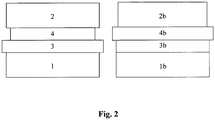
- Figure 2 shows two layer sequences of two semiconductor layers 1 and 2, between which the two layers 3 and 4 of the tunnel diode are sandwiched.
- the different widths of the respective layers indicated in the figures represent the original lattice constant of the materials used in each case for the layers.
- the material of the layer 3 has a relative to the Layer 1 has a larger lattice constant (compressively stressed), while the lattice constant of the material of layer 4 is smaller than the lattice constant of material 3 (tensile stressed).
- the material of layer 2 has a lattice constant that is approximately the same as the material used for layer 1.
- both layer 3 is tensioned on layer 1 and layer 4 is tensioned on layer 3.
- This achieves stress compensation of layers 3, 4, the mean lattice constant of which corresponds approximately to that of the semiconductor layer.
- the material used for layer 3 of the tunnel diode has a lattice constant that is approximately the same as that of the material used for layer 1 of the semiconductor composite. Tensions therefore occur at the transition from layer 3 to layer 4 and from layer 4 to layer 2.
- the material for layer 4 has a larger lattice constant than the materials used for layers 3 and 2, respectively.
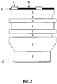
- Figure 3 shows a possible embodiment of a voltage-compensated semiconductor component in a metamorphic triple solar cell structure with GaInP top cell 2, GaInAs middle cell 1, GaInAs buffer structure 6 and Ge substrate 5.
- voltage-compensated tunnel diode layers for example GaInAs 3 and AlGaAs 4 or AlGaAsSb 7 and GaAs 8 can be used.
- the lattice constant is illustrated by the different widths of the boxes.
- the solar cell structure does not have to be metamorphic. Then a buffer layer 6 is not absolutely necessary and the respective indium contents of the partial cells are different depending on the substrate. The layer thickness of the voltage-compensated tunnel diodes must also be adapted accordingly.
- the buffer layer or the tunnel diode layers could also be used for the partial cells of the multiple solar cell, the buffer layer or the tunnel diode layers.
- AlGaInP 2, AlGaInAs 1 and GaInNAs 5 or the tunnel diodes are used in double, quadruple or quintuple cells.
- the sub-cells could for example consist of AlGaInP, GaInP, AlGaInAs, GaInAs, and Ge.
- the voltage-compensated tunnel diode can also be used in other optoelectronic components such as lasers (VCSEL with tunnel contact), light-emitting diodes or isolated tunnel diodes.
- the individual layers of the tunnel diode preferably consist of compressively tensioned AlGaInAs and tensile tensioned AlGaInAs, of compressively tensioned AlGaInP and tensile tensioned AlGaInP, of compressively tensioned AlGaInAs and tensile tensioned AlGaInP or of compressively tensioned AlGaInP or compressively tensioned AlGaInAs.
- the voltage-compensated tunnel diode can be used in tandem solar cells with two pn junctions made from GaInP and Ga (In) As, from Ga (In) As and Ge or from AlGa (In) As and Ga (In) As.
- the voltage compensated Tunnel diodes can also be used in triple solar cells with three pn junctions made from GaInP, GaInAs and Ge, from AlGaInAs, GaInAs and Ge, from AlGaInP and GaInAs and Ge.
- a triple solar cell with the voltage-compensated tunnel diode with three pn junctions made from GaInP, GaAs and GaInAs or from AlGaInP, GaAs and GaInAs is also possible.
- the voltage-compensated tunnel diode can also be used in quadruple solar cells with four pn junctions made of (Al) GaInP, (Al) GaInAs, (Al) GaInNAs, and Ge. Furthermore, the voltage-compensated tunnel diode can be used in five or six-axis solar cells with five or six pn junctions made of AlGaInP, GaInP, AlGaInAs, GaInAs, and GaInNAs and / or Ge.
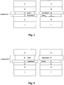
- Figure 4 now shows the same schematic structure as Figure 2 the structure according to the invention of a semiconductor component.
- the structure of the degenerate layers 3, 4 has now been chosen so that one layer, in the example here layer 3, has a greater lattice constant than layer 4, which is symbolically illustrated by the greater width, so that the layer 3 is clamped compressively.
- the layer 4 is grown on tensile-tensioned in order to realize the stress compensation.
- the averaged lattice constant of these layers now essentially corresponds to the lattice constants of the semiconducting materials Layers 1, 2.
- the averaged lattice constant of the layers 4 and 8 in turn corresponds to the lattice constant of the materials of the surrounding semiconducting layers 1, 2.
- the layer 8 is tensile and the other layer 4 is tensioned compressively.
- the barrier layer 8 is compressive and the p-conductive degenerate layer 4 is tensile-tensioned.
- the lattice constants are again adapted here in comparison to the surrounding semiconductor layers 1, 2.
- FIG. 6 shows Figure 6 yet another possibility of how a semiconductor component according to the invention can be constructed.
- a Voltage compensation is now achieved here between the tunnel diode layers 3 and the barrier layers 9.
- the layer 3 is now tensile and the layer 9 is tensioned compressively, whereas in the right part the layer 9 is tensile and the layer 3 is compressively tensioned, here again in comparison to the surrounding semiconductor layers 1, 2, when the averaged material constants are determined, a Alignment is established.
- FIG. 7 now shows an application example in a metamorphic triple solar cell.
- the layers 5 and / or 6 can also consist of several semiconductor layers and possibly form a solar cell.
- the barrier layers 8, 9 of the lower tunnel diode and the barrier layer 8 of the upper tunnel diode are optional.
- Barrier layer 9 of the upper tunnel diode is used in this case for voltage compensation. Compensation means that the mean lattice constant of the stressed layers corresponds to the surrounding semiconductor layers. This also applies in the case of metamorphic structures, where the surrounding semiconductor layers 1, 2 and 7 are meant and not the layers 5 and / or 5a, which have a different or an undefined lattice constant.
Landscapes
- Photovoltaic Devices (AREA)
Claims (11)
- Cellule solaire multi-jonctions comprenant au moins une séquence de couches d'une diode tunnel, qui est disposée en sandwich entre deux couches semi-conductrices (1, 2) et présente des couches dégénérées (3, 4) et éventuellement des couches barrières (8, 9) ayant une épaisseur de couche de 10 nm à 100 nm, qui sont disposées entre les couches dégénérées (3, 4) et les couches semi-conductrices (1, 2), les couches dégénérées (3, 4) étant une couche conductrice n dégénérée (3) ainsi qu'une couche conductrice p dégénérée (4), à la condition que la couche conductrice n dégénérée (3) et la couche conductrice p dégénérée (4) présentent chacune une épaisseur entre 10 nm et 100 nm, cellule dans laquelle, à l'extérieur de l'arrangement en sandwich, au moins l'une des deux couches semi-conductrices (1, 2) est suivie d'une manière itérative d'au moins une diode tunnel supplémentaire, et la diode tunnel supplémentaire est suivie d'au moins une séquence de couches supplémentaire,
la couche conductrice n dégénérée (3) étant compensée en tension avec la couche conductrice p dégénérée (4), ou la couche conductrice n dégénérée (3) ou la couche conductrice p dégénérée (4) étant compensée en tension par rapport à la couche barrière adjacente (8, 9), et les constantes réticulaires des matériaux des couches compensées en tension l'une par rapport à l'autre présentant une différence d'au moins 0,5 %. - Cellule solaire multi-jonctions selon la revendication 1, caractérisée en ce que la différence entre les constantes réticulaires est d'au moins 0,5 % jusqu'à un maximum de 5 %, de préférence d'au moins 1 % jusqu'à un maximum de 2 %.
- Cellule solaire multi-jonctions selon la revendication 1 ou 2, caractérisée en ce que la constante réticulaire moyennée des matériaux des couches compensées en tension les unes par rapport aux autres correspond pour l'essentiel à la constante réticulaire des matériaux des couches semi-conductrices (1, 2).
- Cellule solaire multi-jonctions selon l'une des revendications précédentes, caractérisée en ce que les couches dégénérées (3, 4) sont compensées en tension les unes par rapport aux autres, et la relaxation des dislocations des couches dégénérées (3, 4) est au maximum de 50 %.
- Cellule solaire multi-jonctions selon l'une des revendications précédentes, caractérisée en ce que les couches dégénérées (3, 4) sont compensées en tension les unes par rapport aux autres, et les matériaux des couches semi-conductrices (1, 2) et des couches dégénérées (3, 4) sont, indépendamment les uns des autres, choisis dans le groupe consistant en Ge, Si, SiGe, GaAs, GaSb, GaInP, AlGaAs, GaInAs, GaPN, GaInAsSb, GaInNAs, GaInAsPN, AlGaInP, AlGaInAs, AlGaAsSb, GaAsSb, AlGaSb, InN, GaAsP et/ou AlGaInNAs.
- Cellule solaire multi-jonctions selon l'une des revendications précédentes, caractérisée en ce que les couches dégénérées (3, 4) sont compensées en tension les unes par rapport aux autres, et la couche conductrice p (4) est dopée au carbone et/ou la couche conductrice n (3) est dopée au tellure, au silicium et/ou au germanium.
- Cellule solaire multi-jonctions selon l'une des revendications précédentes, caractérisée en ce qu'au moins l'une des couches barrières (8, 9) présente une énergie de bande interdite supérieure à celle de la couche dégénérée (3, 4) qui lui est adjacente.
- Cellule solaire multi-jonctions selon l'une des revendications précédentes, caractérisée en ce que les couches dégénérées (3, 4) sont compensées en tension les unes par rapport aux autres, et la constante réticulaire moyennée des matériaux des couches dégénérées (3, 4) est pour l'essentiel égale à la constante réticulaire des matériaux des couches semi-conductrices (1, 2).
- Cellule solaire multi-jonctions selon l'une des revendications 1 à 3 ou 7, caractérisée en ce que la couche conductrice n dégénérée (3) ou la couche conductrice p dégénérée (4) est compensée en tension par rapport à la couche barrière adjacente (8, 9), et la constante réticulaire du matériau de la couche dégénérée (3, 4) est supérieure ou inférieure à la couche réticulaire du matériau de la couche barrière (8, 9).
- Cellule solaire multi-jonctions selon la revendication 9, caractérisée en ce que la constante réticulaire moyennée du matériau de la couche dégénérée (3, 4) et du matériau de la couche barrière (8, 9) est pour l'essentiel égale à la constante réticulaire des matériaux des couches semi-conductrices (1, 2).
- Cellule solaire multi-jonctions selon l'une des revendications précédentes, caractérisée en ce que l'au moins l'une des couches semi-conductrices (1, 2)a) est un matériau semi-conducteur à transition p-n, oub) est un matériau semi-conducteur sans transition p-n, à chacun desquels est adjacente au moins une couche semi-conductrice supplémentaire, qui de préférence présente une transition p-n.
Priority Applications (1)
| Application Number | Priority Date | Filing Date | Title |
|---|---|---|---|
| EP10721694.7A EP2430672B1 (fr) | 2009-05-11 | 2010-05-11 | Diodes tunnel composées de couches semi-conductrices de liaison compensées en tension |
Applications Claiming Priority (3)
| Application Number | Priority Date | Filing Date | Title |
|---|---|---|---|
| EP09006342A EP2251912A1 (fr) | 2009-05-11 | 2009-05-11 | Diodes tunnel composées de couches semi-conductrices de liaison compensées en tension |
| PCT/EP2010/002907 WO2010130421A1 (fr) | 2009-05-11 | 2010-05-11 | Diodes tunnel formées de couches semi-conductrices de connexion compensées en tension |
| EP10721694.7A EP2430672B1 (fr) | 2009-05-11 | 2010-05-11 | Diodes tunnel composées de couches semi-conductrices de liaison compensées en tension |
Publications (2)
| Publication Number | Publication Date |
|---|---|
| EP2430672A1 EP2430672A1 (fr) | 2012-03-21 |
| EP2430672B1 true EP2430672B1 (fr) | 2020-12-02 |
Family
ID=41478758
Family Applications (2)
| Application Number | Title | Priority Date | Filing Date |
|---|---|---|---|
| EP09006342A Withdrawn EP2251912A1 (fr) | 2009-05-11 | 2009-05-11 | Diodes tunnel composées de couches semi-conductrices de liaison compensées en tension |
| EP10721694.7A Active EP2430672B1 (fr) | 2009-05-11 | 2010-05-11 | Diodes tunnel composées de couches semi-conductrices de liaison compensées en tension |
Family Applications Before (1)
| Application Number | Title | Priority Date | Filing Date |
|---|---|---|---|
| EP09006342A Withdrawn EP2251912A1 (fr) | 2009-05-11 | 2009-05-11 | Diodes tunnel composées de couches semi-conductrices de liaison compensées en tension |
Country Status (3)
| Country | Link |
|---|---|
| EP (2) | EP2251912A1 (fr) |
| CN (1) | CN102422443B (fr) |
| WO (1) | WO2010130421A1 (fr) |
Families Citing this family (19)
| Publication number | Priority date | Publication date | Assignee | Title |
|---|---|---|---|---|
| CN103022211B (zh) * | 2012-12-28 | 2015-02-11 | 南京大学 | 极化增强的p-i-n结InGaN太阳电池 |
| JP6550691B2 (ja) * | 2013-07-30 | 2019-07-31 | 株式会社リコー | 化合物半導体太陽電池 |
| SG11201606353TA (en) | 2014-02-05 | 2016-09-29 | Solar Junction Corp | Monolithic multijunction power converter |
| ES2749215T3 (es) * | 2014-03-13 | 2020-03-19 | Azur Space Solar Power Gmbh | Célula solar múltiple |
| DE102014113975A1 (de) | 2014-09-26 | 2016-03-31 | Osram Opto Semiconductors Gmbh | Elektronisches Bauelement |
| US11380813B2 (en) | 2019-02-11 | 2022-07-05 | Solaero Technologies Corp. | Metamorphic solar cells |
| DE102017005950A1 (de) * | 2017-06-21 | 2018-12-27 | Azur Space Solar Power Gmbh | Solarzellenstapel |
| WO2019010037A1 (fr) | 2017-07-06 | 2019-01-10 | Solar Junction Corporation | Croissance épitaxiale par mocvd/mbe hybride de cellules solaires à jonctions multiples adaptées au réseau à haut rendement |
| EP3685450A1 (fr) * | 2017-09-18 | 2020-07-29 | Tty-Säätiö Sr. | Structure multicouche semi-conductrice |
| EP3669402A1 (fr) * | 2017-09-27 | 2020-06-24 | Array Photonics, Inc. | Dispositifs optoélectroniques à infrarouge à courte longueur d'onde comportant une couche de nitrure dilué |
| CN108878550B (zh) * | 2018-06-29 | 2020-04-03 | 江苏宜兴德融科技有限公司 | 多结太阳能电池及其制备方法 |
| DE102018009744A1 (de) | 2018-12-14 | 2020-06-18 | Azur Space Solar Power Gmbh | Stapelförmige monolithische aufrecht-metamorphe Mehrfachsolarzelle |
| DE102018009850B4 (de) | 2018-12-19 | 2025-08-21 | Azur Space Solar Power Gmbh | Stapelförmige Mehrfachsolarzelle |
| TWI772587B (zh) * | 2018-12-28 | 2022-08-01 | 晶元光電股份有限公司 | 半導體元件 |
| US11211514B2 (en) | 2019-03-11 | 2021-12-28 | Array Photonics, Inc. | Short wavelength infrared optoelectronic devices having graded or stepped dilute nitride active regions |
| DE102019002034A1 (de) * | 2019-03-22 | 2020-09-24 | Azur Space Solar Power Gmbh | Stapelförmige, monolithische, aufrecht metamorphe, terrestrische Konzentrator-Solarzelle |
| DE102020001185A1 (de) | 2020-02-25 | 2021-08-26 | Azur Space Solar Power Gmbh | Stapelförmige monolithische aufrecht-metamorphe lll-V-Mehrfachsolarzelle |
| EP3965169B1 (fr) | 2020-09-07 | 2023-02-15 | AZUR SPACE Solar Power GmbH | Cellule solaire multiple monolithique empilée |
| EP3965168B1 (fr) | 2020-09-07 | 2023-03-08 | AZUR SPACE Solar Power GmbH | Cellule solaire multiple monolithique empilée |
Family Cites Families (2)
| Publication number | Priority date | Publication date | Assignee | Title |
|---|---|---|---|---|
| US125284A (en) | 1872-04-02 | Improvement in concrete pavements | ||
| US7016392B2 (en) * | 2003-04-30 | 2006-03-21 | Ashish Tandon | GaAs-based long-wavelength laser incorporating tunnel junction structure |
-
2009
- 2009-05-11 EP EP09006342A patent/EP2251912A1/fr not_active Withdrawn
-
2010
- 2010-05-11 EP EP10721694.7A patent/EP2430672B1/fr active Active
- 2010-05-11 WO PCT/EP2010/002907 patent/WO2010130421A1/fr not_active Ceased
- 2010-05-11 CN CN201080020920.XA patent/CN102422443B/zh active Active
Non-Patent Citations (3)
| Title |
|---|
| CARSTEN ROHR ET AL: "InGaAs/InGaAs strain-compensated quantum well cells for thermophotovoltaic applications", PHYSICA E - LOW-DIMENSIONAL SYSTEMS AND NANOSTRUCTURES, vol. 14, no. 1-2, 1 April 2002 (2002-04-01), NL, pages 158 - 161, XP055318260, ISSN: 1386-9477, DOI: 10.1016/S1386-9477(02)00369-7 * |
| FETZER C M ET AL: "High-efficiency metamorphic GaInP/GaInAs/Ge solar cells grown by MOVPE", JOURNAL OF CRYSTAL GROWTH, ELSEVIER, AMSTERDAM, NL, vol. 261, no. 2-3, 19 January 2004 (2004-01-19), pages 341 - 348, XP004484140, ISSN: 0022-0248, DOI: 10.1016/J.JCRYSGRO.2003.11.026 * |
| N.J. EKINS-DAUKES ET AL: "Strain-balanced materials for high-efficiency solar cells", IEEE PHOTOVOLTAIC SPECIALISTS CONFERENCE : PVSC, 1 January 2000 (2000-01-01), US, pages 1273 - 1276, XP055318250, ISSN: 0160-8371, DOI: 10.1109/PVSC.2000.916122 * |
Also Published As
| Publication number | Publication date |
|---|---|
| WO2010130421A1 (fr) | 2010-11-18 |
| EP2251912A1 (fr) | 2010-11-17 |
| CN102422443B (zh) | 2016-04-13 |
| CN102422443A (zh) | 2012-04-18 |
| EP2430672A1 (fr) | 2012-03-21 |
Similar Documents
| Publication | Publication Date | Title |
|---|---|---|
| EP2430672B1 (fr) | Diodes tunnel composées de couches semi-conductrices de liaison compensées en tension | |
| DE102008034711B4 (de) | Invertierte metamorphe Multijunction-Solarzelle mit Barrierenschicht und Verfahren zur Herstellung | |
| WO2013132073A2 (fr) | Cellule solaire multijonction et son utilisation | |
| DE112008002387B4 (de) | Struktur einer Mehrfachübergangs-Solarzelle, Verfahren zur Bildung einer photonischenVorrichtung, Photovoltaische Mehrfachübergangs-Zelle und Photovoltaische Mehrfachübergangs-Zellenvorrichtung, | |
| EP3179521B1 (fr) | Cellule solaire à jonctions multiples | |
| DE102014000156A1 (de) | Mehrfachsolarzelle mit einer einen niedrigen Bandabstand aufweisenden Absorptionsschicht in der Mittelzelle | |
| DE3635944A1 (de) | Tandem-solarzelle | |
| DE102012220933A1 (de) | Mehrfachübergangs-Solarzellen hohen Wirkungsgrades | |
| US20100319764A1 (en) | Functional Integration Of Dilute Nitrides Into High Efficiency III-V Solar Cells | |
| US20120138130A1 (en) | Tunnel diodes comprising stress-compensated compound semiconductor layers | |
| EP2960950B1 (fr) | Cellule solaire à jonctions multiples | |
| DE102017200700A1 (de) | Mehrfachsolarzelle mit rückseitiger Germanium-Teilzelle und deren Verwendung | |
| EP3419060A1 (fr) | Empilement de cellules solaires | |
| DE102018203509B4 (de) | Vierfach-Solarzelle für Raumanwendungen | |
| EP3012874A1 (fr) | Cellule solaire à jonctions multiples intégrée en forme de pile | |
| DE102010010880A1 (de) | Multijunction-Solarzellen basierend auf Gruppe-IV/III-V Hybrid-Halbleiterverbindungen | |
| WO2014111314A1 (fr) | Élément semi-conducteur doté d'un tampon de dureté et son utilisation | |
| WO2013050563A2 (fr) | Composant à semi-conducteurs présentant une structure multicouche et module formé à partir de ce composant | |
| Chevuntulak et al. | Molecular beam epitaxial growth of interdigitated quantum dots for heterojunction solar cells | |
| DE102016005640A1 (de) | Invertierte Mehrfach-Solarzelle | |
| EP3937260A1 (fr) | Cellule solaire multiple métamorphique monolithique | |
| DE102013002298A1 (de) | Mehrfachsolarzelle, Verfahren zu deren Herstellung und Verwendung hiervon | |
| EP3937259A1 (fr) | Cellule solaire multiple métamorphique monolithique | |
| DE102009049397B4 (de) | Herstellungsverfahren mit Surrogatsubstrat für invertierte metamorphische Multijunction-Solarzellen | |
| DE102019002034A1 (de) | Stapelförmige, monolithische, aufrecht metamorphe, terrestrische Konzentrator-Solarzelle |
Legal Events
| Date | Code | Title | Description |
|---|---|---|---|
| PUAI | Public reference made under article 153(3) epc to a published international application that has entered the european phase |
Free format text: ORIGINAL CODE: 0009012 |
|
| 17P | Request for examination filed |
Effective date: 20111102 |
|
| AK | Designated contracting states |
Kind code of ref document: A1 Designated state(s): AL AT BE BG CH CY CZ DE DK EE ES FI FR GB GR HR HU IE IS IT LI LT LU LV MC MK MT NL NO PL PT RO SE SI SK SM TR |
|
| RIN1 | Information on inventor provided before grant (corrected) |
Inventor name: SCHOENE, JAN Inventor name: DIMROTH, FRANK Inventor name: GUTER, WOLFGANG |
|
| DAX | Request for extension of the european patent (deleted) | ||
| STAA | Information on the status of an ep patent application or granted ep patent |
Free format text: STATUS: EXAMINATION IS IN PROGRESS |
|
| 17Q | First examination report despatched |
Effective date: 20161117 |
|
| REG | Reference to a national code |
Ref country code: DE Ref legal event code: R079 Ref document number: 502010016809 Country of ref document: DE Free format text: PREVIOUS MAIN CLASS: H01L0031068000 Ipc: H01L0031068700 |
|
| GRAP | Despatch of communication of intention to grant a patent |
Free format text: ORIGINAL CODE: EPIDOSNIGR1 |
|
| STAA | Information on the status of an ep patent application or granted ep patent |
Free format text: STATUS: GRANT OF PATENT IS INTENDED |
|
| RIC1 | Information provided on ipc code assigned before grant |
Ipc: H01S 5/30 20060101ALN20200626BHEP Ipc: H01L 33/00 20100101ALN20200626BHEP Ipc: H01S 5/183 20060101ALI20200626BHEP Ipc: H01L 33/30 20100101ALI20200626BHEP Ipc: H01L 29/885 20060101ALI20200626BHEP Ipc: H01L 29/88 20060101ALN20200626BHEP Ipc: H01L 31/0687 20120101AFI20200626BHEP Ipc: H01L 33/06 20100101ALI20200626BHEP Ipc: H01L 33/04 20100101ALI20200626BHEP |
|
| INTG | Intention to grant announced |
Effective date: 20200721 |
|
| GRAS | Grant fee paid |
Free format text: ORIGINAL CODE: EPIDOSNIGR3 |
|
| GRAA | (expected) grant |
Free format text: ORIGINAL CODE: 0009210 |
|
| STAA | Information on the status of an ep patent application or granted ep patent |
Free format text: STATUS: THE PATENT HAS BEEN GRANTED |
|
| AK | Designated contracting states |
Kind code of ref document: B1 Designated state(s): AL AT BE BG CH CY CZ DE DK EE ES FI FR GB GR HR HU IE IS IT LI LT LU LV MC MK MT NL NO PL PT RO SE SI SK SM TR |
|
| REG | Reference to a national code |
Ref country code: GB Ref legal event code: FG4D Free format text: NOT ENGLISH |
|
| REG | Reference to a national code |
Ref country code: AT Ref legal event code: REF Ref document number: 1341874 Country of ref document: AT Kind code of ref document: T Effective date: 20201215 Ref country code: CH Ref legal event code: EP |
|
| REG | Reference to a national code |
Ref country code: DE Ref legal event code: R096 Ref document number: 502010016809 Country of ref document: DE |
|
| REG | Reference to a national code |
Ref country code: IE Ref legal event code: FG4D Free format text: LANGUAGE OF EP DOCUMENT: GERMAN |
|
| PG25 | Lapsed in a contracting state [announced via postgrant information from national office to epo] |
Ref country code: GR Free format text: LAPSE BECAUSE OF FAILURE TO SUBMIT A TRANSLATION OF THE DESCRIPTION OR TO PAY THE FEE WITHIN THE PRESCRIBED TIME-LIMIT Effective date: 20210303 Ref country code: NO Free format text: LAPSE BECAUSE OF FAILURE TO SUBMIT A TRANSLATION OF THE DESCRIPTION OR TO PAY THE FEE WITHIN THE PRESCRIBED TIME-LIMIT Effective date: 20210302 Ref country code: FI Free format text: LAPSE BECAUSE OF FAILURE TO SUBMIT A TRANSLATION OF THE DESCRIPTION OR TO PAY THE FEE WITHIN THE PRESCRIBED TIME-LIMIT Effective date: 20201202 |
|
| REG | Reference to a national code |
Ref country code: NL Ref legal event code: MP Effective date: 20201202 |
|
| PG25 | Lapsed in a contracting state [announced via postgrant information from national office to epo] |
Ref country code: SE Free format text: LAPSE BECAUSE OF FAILURE TO SUBMIT A TRANSLATION OF THE DESCRIPTION OR TO PAY THE FEE WITHIN THE PRESCRIBED TIME-LIMIT Effective date: 20201202 Ref country code: PL Free format text: LAPSE BECAUSE OF FAILURE TO SUBMIT A TRANSLATION OF THE DESCRIPTION OR TO PAY THE FEE WITHIN THE PRESCRIBED TIME-LIMIT Effective date: 20201202 Ref country code: LV Free format text: LAPSE BECAUSE OF FAILURE TO SUBMIT A TRANSLATION OF THE DESCRIPTION OR TO PAY THE FEE WITHIN THE PRESCRIBED TIME-LIMIT Effective date: 20201202 Ref country code: BG Free format text: LAPSE BECAUSE OF FAILURE TO SUBMIT A TRANSLATION OF THE DESCRIPTION OR TO PAY THE FEE WITHIN THE PRESCRIBED TIME-LIMIT Effective date: 20210302 |
|
| PG25 | Lapsed in a contracting state [announced via postgrant information from national office to epo] |
Ref country code: HR Free format text: LAPSE BECAUSE OF FAILURE TO SUBMIT A TRANSLATION OF THE DESCRIPTION OR TO PAY THE FEE WITHIN THE PRESCRIBED TIME-LIMIT Effective date: 20201202 Ref country code: NL Free format text: LAPSE BECAUSE OF FAILURE TO SUBMIT A TRANSLATION OF THE DESCRIPTION OR TO PAY THE FEE WITHIN THE PRESCRIBED TIME-LIMIT Effective date: 20201202 |
|
| REG | Reference to a national code |
Ref country code: LT Ref legal event code: MG9D |
|
| PG25 | Lapsed in a contracting state [announced via postgrant information from national office to epo] |
Ref country code: LT Free format text: LAPSE BECAUSE OF FAILURE TO SUBMIT A TRANSLATION OF THE DESCRIPTION OR TO PAY THE FEE WITHIN THE PRESCRIBED TIME-LIMIT Effective date: 20201202 Ref country code: CZ Free format text: LAPSE BECAUSE OF FAILURE TO SUBMIT A TRANSLATION OF THE DESCRIPTION OR TO PAY THE FEE WITHIN THE PRESCRIBED TIME-LIMIT Effective date: 20201202 Ref country code: EE Free format text: LAPSE BECAUSE OF FAILURE TO SUBMIT A TRANSLATION OF THE DESCRIPTION OR TO PAY THE FEE WITHIN THE PRESCRIBED TIME-LIMIT Effective date: 20201202 Ref country code: RO Free format text: LAPSE BECAUSE OF FAILURE TO SUBMIT A TRANSLATION OF THE DESCRIPTION OR TO PAY THE FEE WITHIN THE PRESCRIBED TIME-LIMIT Effective date: 20201202 Ref country code: SK Free format text: LAPSE BECAUSE OF FAILURE TO SUBMIT A TRANSLATION OF THE DESCRIPTION OR TO PAY THE FEE WITHIN THE PRESCRIBED TIME-LIMIT Effective date: 20201202 Ref country code: PT Free format text: LAPSE BECAUSE OF FAILURE TO SUBMIT A TRANSLATION OF THE DESCRIPTION OR TO PAY THE FEE WITHIN THE PRESCRIBED TIME-LIMIT Effective date: 20210405 Ref country code: SM Free format text: LAPSE BECAUSE OF FAILURE TO SUBMIT A TRANSLATION OF THE DESCRIPTION OR TO PAY THE FEE WITHIN THE PRESCRIBED TIME-LIMIT Effective date: 20201202 |
|
| REG | Reference to a national code |
Ref country code: DE Ref legal event code: R097 Ref document number: 502010016809 Country of ref document: DE |
|
| PG25 | Lapsed in a contracting state [announced via postgrant information from national office to epo] |
Ref country code: IS Free format text: LAPSE BECAUSE OF FAILURE TO SUBMIT A TRANSLATION OF THE DESCRIPTION OR TO PAY THE FEE WITHIN THE PRESCRIBED TIME-LIMIT Effective date: 20210402 |
|
| PLBE | No opposition filed within time limit |
Free format text: ORIGINAL CODE: 0009261 |
|
| STAA | Information on the status of an ep patent application or granted ep patent |
Free format text: STATUS: NO OPPOSITION FILED WITHIN TIME LIMIT |
|
| PG25 | Lapsed in a contracting state [announced via postgrant information from national office to epo] |
Ref country code: AL Free format text: LAPSE BECAUSE OF FAILURE TO SUBMIT A TRANSLATION OF THE DESCRIPTION OR TO PAY THE FEE WITHIN THE PRESCRIBED TIME-LIMIT Effective date: 20201202 |
|
| 26N | No opposition filed |
Effective date: 20210903 |
|
| PG25 | Lapsed in a contracting state [announced via postgrant information from national office to epo] |
Ref country code: ES Free format text: LAPSE BECAUSE OF FAILURE TO SUBMIT A TRANSLATION OF THE DESCRIPTION OR TO PAY THE FEE WITHIN THE PRESCRIBED TIME-LIMIT Effective date: 20201202 Ref country code: DK Free format text: LAPSE BECAUSE OF FAILURE TO SUBMIT A TRANSLATION OF THE DESCRIPTION OR TO PAY THE FEE WITHIN THE PRESCRIBED TIME-LIMIT Effective date: 20201202 Ref country code: SI Free format text: LAPSE BECAUSE OF FAILURE TO SUBMIT A TRANSLATION OF THE DESCRIPTION OR TO PAY THE FEE WITHIN THE PRESCRIBED TIME-LIMIT Effective date: 20201202 |
|
| REG | Reference to a national code |
Ref country code: CH Ref legal event code: PL |
|
| GBPC | Gb: european patent ceased through non-payment of renewal fee |
Effective date: 20210511 |
|
| PG25 | Lapsed in a contracting state [announced via postgrant information from national office to epo] |
Ref country code: LU Free format text: LAPSE BECAUSE OF NON-PAYMENT OF DUE FEES Effective date: 20210511 Ref country code: LI Free format text: LAPSE BECAUSE OF NON-PAYMENT OF DUE FEES Effective date: 20210531 Ref country code: MC Free format text: LAPSE BECAUSE OF FAILURE TO SUBMIT A TRANSLATION OF THE DESCRIPTION OR TO PAY THE FEE WITHIN THE PRESCRIBED TIME-LIMIT Effective date: 20201202 Ref country code: CH Free format text: LAPSE BECAUSE OF NON-PAYMENT OF DUE FEES Effective date: 20210531 |
|
| REG | Reference to a national code |
Ref country code: BE Ref legal event code: MM Effective date: 20210531 |
|
| PG25 | Lapsed in a contracting state [announced via postgrant information from national office to epo] |
Ref country code: IE Free format text: LAPSE BECAUSE OF NON-PAYMENT OF DUE FEES Effective date: 20210511 Ref country code: GB Free format text: LAPSE BECAUSE OF NON-PAYMENT OF DUE FEES Effective date: 20210511 |
|
| PG25 | Lapsed in a contracting state [announced via postgrant information from national office to epo] |
Ref country code: IS Free format text: LAPSE BECAUSE OF FAILURE TO SUBMIT A TRANSLATION OF THE DESCRIPTION OR TO PAY THE FEE WITHIN THE PRESCRIBED TIME-LIMIT Effective date: 20210402 |
|
| REG | Reference to a national code |
Ref country code: AT Ref legal event code: MM01 Ref document number: 1341874 Country of ref document: AT Kind code of ref document: T Effective date: 20210511 |
|
| PG25 | Lapsed in a contracting state [announced via postgrant information from national office to epo] |
Ref country code: BE Free format text: LAPSE BECAUSE OF NON-PAYMENT OF DUE FEES Effective date: 20210531 |
|
| PG25 | Lapsed in a contracting state [announced via postgrant information from national office to epo] |
Ref country code: AT Free format text: LAPSE BECAUSE OF NON-PAYMENT OF DUE FEES Effective date: 20210511 |
|
| PG25 | Lapsed in a contracting state [announced via postgrant information from national office to epo] |
Ref country code: HU Free format text: LAPSE BECAUSE OF FAILURE TO SUBMIT A TRANSLATION OF THE DESCRIPTION OR TO PAY THE FEE WITHIN THE PRESCRIBED TIME-LIMIT; INVALID AB INITIO Effective date: 20100511 Ref country code: CY Free format text: LAPSE BECAUSE OF FAILURE TO SUBMIT A TRANSLATION OF THE DESCRIPTION OR TO PAY THE FEE WITHIN THE PRESCRIBED TIME-LIMIT Effective date: 20201202 |
|
| P01 | Opt-out of the competence of the unified patent court (upc) registered |
Effective date: 20230524 |
|
| PG25 | Lapsed in a contracting state [announced via postgrant information from national office to epo] |
Ref country code: MK Free format text: LAPSE BECAUSE OF FAILURE TO SUBMIT A TRANSLATION OF THE DESCRIPTION OR TO PAY THE FEE WITHIN THE PRESCRIBED TIME-LIMIT Effective date: 20201202 |
|
| PG25 | Lapsed in a contracting state [announced via postgrant information from national office to epo] |
Ref country code: MT Free format text: LAPSE BECAUSE OF FAILURE TO SUBMIT A TRANSLATION OF THE DESCRIPTION OR TO PAY THE FEE WITHIN THE PRESCRIBED TIME-LIMIT Effective date: 20201202 |
|
| REG | Reference to a national code |
Ref country code: DE Ref legal event code: R079 Ref document number: 502010016809 Country of ref document: DE Free format text: PREVIOUS MAIN CLASS: H01L0031068700 Ipc: H10F0010142000 |
|
| PGFP | Annual fee paid to national office [announced via postgrant information from national office to epo] |
Ref country code: DE Payment date: 20250519 Year of fee payment: 16 |
|
| PGFP | Annual fee paid to national office [announced via postgrant information from national office to epo] |
Ref country code: IT Payment date: 20250530 Year of fee payment: 16 |
|
| PGFP | Annual fee paid to national office [announced via postgrant information from national office to epo] |
Ref country code: FR Payment date: 20250521 Year of fee payment: 16 |
|
| PG25 | Lapsed in a contracting state [announced via postgrant information from national office to epo] |
Ref country code: TR Free format text: LAPSE BECAUSE OF FAILURE TO SUBMIT A TRANSLATION OF THE DESCRIPTION OR TO PAY THE FEE WITHIN THE PRESCRIBED TIME-LIMIT Effective date: 20201202 |