EP3419060A1 - Empilement de cellules solaires - Google Patents
Empilement de cellules solaires Download PDFInfo
- Publication number
- EP3419060A1 EP3419060A1 EP18000531.6A EP18000531A EP3419060A1 EP 3419060 A1 EP3419060 A1 EP 3419060A1 EP 18000531 A EP18000531 A EP 18000531A EP 3419060 A1 EP3419060 A1 EP 3419060A1
- Authority
- EP
- European Patent Office
- Prior art keywords
- layer
- solar cell
- subcell
- lattice constant
- tunnel diode
- Prior art date
- Legal status (The legal status is an assumption and is not a legal conclusion. Google has not performed a legal analysis and makes no representation as to the accuracy of the status listed.)
- Granted
Links
Images


Classifications
-
- H—ELECTRICITY
- H10—SEMICONDUCTOR DEVICES; ELECTRIC SOLID-STATE DEVICES NOT OTHERWISE PROVIDED FOR
- H10F—INORGANIC SEMICONDUCTOR DEVICES SENSITIVE TO INFRARED RADIATION, LIGHT, ELECTROMAGNETIC RADIATION OF SHORTER WAVELENGTH OR CORPUSCULAR RADIATION
- H10F10/00—Individual photovoltaic cells, e.g. solar cells
- H10F10/10—Individual photovoltaic cells, e.g. solar cells having potential barriers
- H10F10/16—Photovoltaic cells having only PN heterojunction potential barriers
- H10F10/161—Photovoltaic cells having only PN heterojunction potential barriers comprising multiple PN heterojunctions, e.g. tandem cells
-
- H—ELECTRICITY
- H10—SEMICONDUCTOR DEVICES; ELECTRIC SOLID-STATE DEVICES NOT OTHERWISE PROVIDED FOR
- H10F—INORGANIC SEMICONDUCTOR DEVICES SENSITIVE TO INFRARED RADIATION, LIGHT, ELECTROMAGNETIC RADIATION OF SHORTER WAVELENGTH OR CORPUSCULAR RADIATION
- H10F19/00—Integrated devices, or assemblies of multiple devices, comprising at least one photovoltaic cell covered by group H10F10/00, e.g. photovoltaic modules
- H10F19/40—Integrated devices, or assemblies of multiple devices, comprising at least one photovoltaic cell covered by group H10F10/00, e.g. photovoltaic modules comprising photovoltaic cells in a mechanically stacked configuration
-
- H—ELECTRICITY
- H10—SEMICONDUCTOR DEVICES; ELECTRIC SOLID-STATE DEVICES NOT OTHERWISE PROVIDED FOR
- H10F—INORGANIC SEMICONDUCTOR DEVICES SENSITIVE TO INFRARED RADIATION, LIGHT, ELECTROMAGNETIC RADIATION OF SHORTER WAVELENGTH OR CORPUSCULAR RADIATION
- H10F10/00—Individual photovoltaic cells, e.g. solar cells
- H10F10/10—Individual photovoltaic cells, e.g. solar cells having potential barriers
- H10F10/14—Photovoltaic cells having only PN homojunction potential barriers
- H10F10/142—Photovoltaic cells having only PN homojunction potential barriers comprising multiple PN homojunctions, e.g. tandem cells
-
- H—ELECTRICITY
- H10—SEMICONDUCTOR DEVICES; ELECTRIC SOLID-STATE DEVICES NOT OTHERWISE PROVIDED FOR
- H10F—INORGANIC SEMICONDUCTOR DEVICES SENSITIVE TO INFRARED RADIATION, LIGHT, ELECTROMAGNETIC RADIATION OF SHORTER WAVELENGTH OR CORPUSCULAR RADIATION
- H10F10/00—Individual photovoltaic cells, e.g. solar cells
- H10F10/10—Individual photovoltaic cells, e.g. solar cells having potential barriers
- H10F10/16—Photovoltaic cells having only PN heterojunction potential barriers
- H10F10/163—Photovoltaic cells having only PN heterojunction potential barriers comprising only Group III-V materials, e.g. GaAs/AlGaAs or InP/GaInAs photovoltaic cells
-
- H—ELECTRICITY
- H10—SEMICONDUCTOR DEVICES; ELECTRIC SOLID-STATE DEVICES NOT OTHERWISE PROVIDED FOR
- H10F—INORGANIC SEMICONDUCTOR DEVICES SENSITIVE TO INFRARED RADIATION, LIGHT, ELECTROMAGNETIC RADIATION OF SHORTER WAVELENGTH OR CORPUSCULAR RADIATION
- H10F19/00—Integrated devices, or assemblies of multiple devices, comprising at least one photovoltaic cell covered by group H10F10/00, e.g. photovoltaic modules
- H10F19/10—Integrated devices, or assemblies of multiple devices, comprising at least one photovoltaic cell covered by group H10F10/00, e.g. photovoltaic modules comprising photovoltaic cells in arrays in a single semiconductor substrate, the photovoltaic cells having vertical junctions or V-groove junctions
-
- H—ELECTRICITY
- H10—SEMICONDUCTOR DEVICES; ELECTRIC SOLID-STATE DEVICES NOT OTHERWISE PROVIDED FOR
- H10F—INORGANIC SEMICONDUCTOR DEVICES SENSITIVE TO INFRARED RADIATION, LIGHT, ELECTROMAGNETIC RADIATION OF SHORTER WAVELENGTH OR CORPUSCULAR RADIATION
- H10F77/00—Constructional details of devices covered by this subclass
- H10F77/10—Semiconductor bodies
- H10F77/12—Active materials
- H10F77/124—Active materials comprising only Group III-V materials, e.g. GaAs
- H10F77/1248—Active materials comprising only Group III-V materials, e.g. GaAs having three or more elements, e.g. GaAlAs, InGaAs or InGaAsP
-
- Y—GENERAL TAGGING OF NEW TECHNOLOGICAL DEVELOPMENTS; GENERAL TAGGING OF CROSS-SECTIONAL TECHNOLOGIES SPANNING OVER SEVERAL SECTIONS OF THE IPC; TECHNICAL SUBJECTS COVERED BY FORMER USPC CROSS-REFERENCE ART COLLECTIONS [XRACs] AND DIGESTS
- Y02—TECHNOLOGIES OR APPLICATIONS FOR MITIGATION OR ADAPTATION AGAINST CLIMATE CHANGE
- Y02E—REDUCTION OF GREENHOUSE GAS [GHG] EMISSIONS, RELATED TO ENERGY GENERATION, TRANSMISSION OR DISTRIBUTION
- Y02E10/00—Energy generation through renewable energy sources
- Y02E10/50—Photovoltaic [PV] energy
- Y02E10/544—Solar cells from Group III-V materials
-
- Y—GENERAL TAGGING OF NEW TECHNOLOGICAL DEVELOPMENTS; GENERAL TAGGING OF CROSS-SECTIONAL TECHNOLOGIES SPANNING OVER SEVERAL SECTIONS OF THE IPC; TECHNICAL SUBJECTS COVERED BY FORMER USPC CROSS-REFERENCE ART COLLECTIONS [XRACs] AND DIGESTS
- Y02—TECHNOLOGIES OR APPLICATIONS FOR MITIGATION OR ADAPTATION AGAINST CLIMATE CHANGE
- Y02P—CLIMATE CHANGE MITIGATION TECHNOLOGIES IN THE PRODUCTION OR PROCESSING OF GOODS
- Y02P70/00—Climate change mitigation technologies in the production process for final industrial or consumer products
- Y02P70/50—Manufacturing or production processes characterised by the final manufactured product
Definitions
- the invention relates to a solar cell stack.
- From the EP 2 251 912 A1 is a stacked monolithic multiple solar cell with improved power line between the solar cells known.
- a tunnel diode with mutually strained degenerate layers is arranged between two successive solar cells.
- a tensilely strained degenerated layer is compensated with a compressively strained degenerate layer.
- the degenerate layers are designed either as degenerate p + doped with carbon or as degenerate n + layers doped with tellurium or silicon.
- the degenerate layers of the tunnel diode are included for voltage compensation. While the degenerate n + layer is always unstrained and the Lattice constant of the immediately adjacent barrier layer, in the present case, the degenerate p + layer is always tensioned either tensil or compressively. Accordingly, the voltage applied to the degenerate p + layer barrier layer is compressed or tensile tensed. By compensating the strain again, no strain acts on the layers surrounding the barrier layer, in other words the sum of the strain is zero.
- the typical procedure for tunnel diode materials of new solar cell concepts with metamorphic buffers is a lattice matching of the tunnel diode layers to the substrate lattice constant or to the new virtual substrate lattice constant in metamorphic structures.
- the tunnel diode layers should have a sufficiently high doping for the current carrying capacity and a sufficiently high transparency for underlying sub-cells.
- the degenerate p + layer plastically relaxes and induces thread dislocations or cracks and reduces the efficiency of the metamorphic multiple solar cell.
- An alternative p-doped tunnel diode material is (Al) GaAsSb.
- This material system can be adapted to different lattice constants by the As / Sb ratio and at the same time highly p-doped (e.g., intrinsic carbon or CBr4 doping).
- (Al) GaAsSb is thus used to produce lattice-matched tunnel diode structures.
- MOVPE organometallic vapor phase epitaxy
- the object of the invention is to provide a device which further develops the prior art and in particular increases the efficiency of the metamorphic solar cells by a better lattice matching of the p + layer and at the same time reduces the current carrying capacity of the tunnel diode as little as possible.
- a solar cell stack is provided with a predominant number of III-V semiconductor layers, wherein the solar cell stack has a first partial cell with a first bandgap and with a first lattice constant, and a second partial cell with a second bandgap and with a second lattice constant.
- the interlayer sequence has a first barrier layer and a first tunnel diode and a second barrier layer, wherein the layers are arranged in said order.
- the tunnel diode has a degenerate n + layer with a third lattice constant and a degenerate p + layer with a fourth lattice constant, wherein the fourth lattice constant is less than the third lattice constant and the first bandgap is less than the second bandgap and the p + layer has a different material composition with indium than the n + layer.
- the n + layer is disposed between the first barrier layer and the p + layer.
- the p + layer is disposed between the n + layer and the second barrier layer.
- the first subcell and the second subcell are lattice matched, and the p + layer has a smaller lattice constant with a lattice mismatch of at least 0.5%.
- a metamorphic buffer is formed between the first subcell and the second subcell, wherein the degenerate p + layer of the tunnel diode is lattice-matched neither to the first subcell nor to the second subcell.
- the fourth lattice constant is between the first lattice constant and the second lattice constant.
- the third lattice constant of the degenerate n + layer of the tunnel diode is lattice-matched to the first subcell or to the second subcell.
- the degenerate p + layer has a different material combination than the degenerate n + layer.
- the degenerate p + layer contains at least 5% indium and as carbon dopant.
- the layers of the tunnel diode and the further layers of the interlayer sequence are not voltage-compensated with respect to one another.
- lattice matching is understood to mean a difference in lattice constants of two consecutive layers smaller than 0.1%.
- non-stress-compensated means that a strain is generated by the lattice mismatch of the degenerate p + layer and the stress is not compensated by the degenerate n + layer or by the barrier layers.
- the third lattice constant or lattice constants of the two barrier layers are equal to either the first lattice constant or equal to the second lattice constant.
- III-V semiconductor layers refers to a multiple solar cell, of which layers more than 50%, preferably more than 80%, consist of III-V materials.
- such a subcell often also includes a Ge subcell, the further subcells of the solar cell stack consisting of the III-V materials or compounds.
- the term sub-cell is used interchangeably with the term of the sub-solar cell.
- the solar cell stack consists of a plurality of partial solar cells, which are interconnected in series by means of tunnel diodes.
- material composition for example an InGaAs material composition, denotes a compound of the cited elements, wherein in addition to the cited elements also other elements may be included.
- degenerate layer in the present case means a highly doped tunnel diode layer.
- the concept of degeneracy thus refers to the fact that the Fermi level of the n + layer is in the conduction band and the Fermi level of the p + layer is in the valence band, i. the semiconductor layers have a metallic conductivity.
- the layers directly surrounding the tunnel diode are not stressed. Based on the interlayer sequence, only the degenerate p.sup. + Layer of the tunnel diode is lattice-mismatched with respect to the barrier layers or with respect to at least one of the lattice constants of the sub-cells and thus has a tensile stress. In other words, the barrier layers have the lattice constants of adjacent sub-cells.
- a compromise can be achieved from sufficiently high lattice matching and sufficiently high p-doping and sufficiently high transparency of the p + layer.
- the plastic relaxation of the p + layer is avoided with the formation of dislocations or cracks and increases the material quality of the adjacent sub-cells.
- the efficiency of the multi-junction metamorphic cell is increased.
- Another advantage is that by means of both alternatives can reduce the strain and thereby the curvature of the wafer.
- n + -layer lattice-matched to one of the sub-cells or to both sub-cells ie having the same or nearly the same lattice constant as a subcell or both subcells, always assumes a tensile strain from the p + layer of the tunnel diode and thereby from the interlayer sequence. That is, the p + layer of the tunnel diode is tensilely tensed, the surrounding layers are lattice-matched to one of the sub-cells or to both sub-cells and thus unstrained.
- the bracing is thus not compensated in the intermediate layer sequence, but preferably at least partially by other layers of the solar cell stack.
- One advantage is that with the tensioning of the p.sup. + Layer, the compressive stresses incorporated during the epitaxy process both before the production and after the production of the intermediate layer sequence are at least partially compensated.
- Another advantage, in particular of the second alternative, is that even with a metamorphic buffer between the first subcell and the second subcell and the rest of the wafer resulting from the installation of the buffer by means of the degenerate p + layer of the tunnel diode whose lattice constant neither the first subcell is lattice matched yet to the second subcell, can perform an at least partial compensation.
- the degenerate p + layer of the tunnel diode has a lattice mismatch to the degenerate n + layer of the tunnel diode between 0.5% and 2.0%.
- the degenerate p + layer of the tunnel diode consists of a material composition of AlInGaAs, wherein the carbon concentration in the material is greater than 1E19 cm-3.
- the indium content of the degenerate p + -type AlInGaAs layer of the tunnel diode is between 5% and 20%, the aluminum content of the degenerate p + -conducting layer being between 10% and 80%.
- the lattice constant of the degenerate p + -type layer of the tunnel diode is between 5,674 A and 5,734 A.
- the lattice constant is also influenced by the indium content.
- the degenerate p + layer of the tunnel diode contains no antimony or up to a maximum of 5% antimony.
- the degenerate n + -type layer of the tunnel diode consists of a compound of InGaP or AlInGaP or AlInP and is doped with tellurium, silicon, selenium or germanium, the lattice constant being between 5,714 ⁇ and 5,785 ⁇ .
- the indium content of the degenerate n + -type layer of the tunnel diode is between 63% and 80%.
- the aluminum content is a maximum of 37%.
- the indium content for InAlP is max. 63% and the aluminum content at max. 37%.
- the indium content for InAlP is about 70% and the aluminum content at max. about 30%.
- the indium content is X and the aluminum content is Y, and this gives, for example, an X value of 0.15 for an indium content of 15% and for a maximum aluminum content of 85%, a maximum Y value of 0.85.
- the solar cell stack comprises a Ge or a GaAs substrate.
- the Ge substrate is at the top, i. against the direction of light incidence on an n-doped layer.
- the Ge subcell is formed as the lowest subcell.
- the solar cell stack comprises exactly three subcells, wherein a further tunnel diode is formed between the second subcell and the third subcell. It is understood that the tensions the two tunnel diodes do not compensate. Alternatively, only one of the two tunnel diodes is braced. Preferably, the tunnel diode between the second subcell and the third subcell is not clamped.
- the strained tunnel diode is present once or twice. It is understood that the strained tunnel diodes are each arranged between two directly successive sub-cells. Preferably, three of the four sub-cells are located above the metamorphic buffer. Preferably, an undamped tunnel diode is formed between the lowermost subcell and the metamorphic buffer.
- the strained tunnel diode is present one to three times in the stack-shaped upright metamorphic fourfold multiple solar cell.
- One of the strained tunneling diode is located between the metamorphic buffer and the subcell above the metamorphic buffer.
- Three of the four sub-cells are arranged above the metamorphic buffer, wherein in each case a strained tunnel diode is arranged between adjacent sub-cells.
- individual strained tunnel diodes can be replaced by grid-tuned tunnel diodes or other tunnel diodes.
- the strained tunnel diode is present one to three times in the stacked upright metamorphic five times multiple solar cell, and is located between each two sub-cells, with four of the five sub-cells located above the metamorphic buffer.
- an undamped tunnel diode is formed between the lowermost subcell and the metamorphic buffer.
- individual strained tunnel diodes can be replaced by grid-tuned tunnel diodes or other tunnel diodes.
- the strained tunnel diode is present one to four times in a stack-shaped upright metamorphic five times multiple solar cell, wherein four of the five sub-cells are located above the metamorphic buffer.
- the strained tunnel diode is formed between the metamorphic buffer and the adjoining sub-cell and arranged in each case between two adjacent sub-cells above the metamorphic buffer.
- individual strained tunnel diodes can be replaced by grid-tuned tunnel diodes or other tunnel diodes.
- the layers of the metamorphic buffer in the second embodiment consist of material compositions of InGaAs and / or AlInGaAs and / or InGaP, wherein the metamorphic buffer has a sequence of at least three layers and the lattice constant in the sequence towards the second subcell of Layer to layer increases and wherein the lattice constants of the layers of the buffer are greater than the lattice constant of the first subcell and wherein a layer of the metamorphic buffer has a third lattice constant and the third lattice constant is greater than the lattice constant of the second subcell.
- the metamorphic buffer has a sequence of at least five layers or exactly five layers. In one development, one of the layers has a compressive strain in the metamorphic buffer.
- the degenerate p + layer of the tunnel diode is voltage-compensated neither by a layer following in relation to the tunnel diode nor by a layer preceding it with respect to the tunnel diode. It is understood that the term of the subsequent layers hereby denotes layers which are deposited during the epitaxial process only after the p + layer.
- the solar cell stack is monolithic.
- novel tunnel diode which generates a tensile strain, can be advantageously used both in upright and inverted grown multiple solar cells.
- the FIG. 1 shows a solar cell stack ST with a first subcell SC1 and a second subcell SC2 and with a tunnel diode according to the invention TD1.
- the solar cell stack ST has predominantly III-V semiconductor layers. In this case, the light incidence L takes place through the second solar cell SC2.
- the size of the lattice constant a is illustrated by an arrow.
- the illustrated lateral extent of the individual layers, ie the extent in the direction of the arrow corresponds to the size of the lattice constant.
- the first subcell SC1 has a first bandgap with a first lattice constant.
- the second subcell SC2 has a second bandgap with a second lattice constant.
- the second subcell SC2 has an equal to or greater band gap than the first subcell SC1.
- the interlayer sequence ZF has a first barrier layer B1 and the tunnel diode TD1 with a degenerate n + layer with a third lattice constant and a degenerate p + layer with a fourth lattice constant and a second barrier layer B2, wherein the layers are arranged in the named order.
- the fourth lattice constant is smaller than the third lattice constant.
- the first bandgap is smaller than the second bandgap.
- the degenerate p + layer has a different material composition than the degenerate n + layer.
- the p + layer has a smaller lattice constant with a lattice mismatch of at least 0.5% to the n + layer.
- the layers of the tunnel diode TD1 and the further layers of the interlayer sequence ZF i. the two barrier layers B1 and B2 are not voltage-compensated to one another.
- the degenerate p + layer contains not only indium but also carbon as a dopant.
- the first subcell SC1 and the second subcell SC2 are lattice-matched to one another, i. the two lattice constants are the same.
- the degenerate n + layer is also lattice-matched to the two subcells SC1 and SC2.
- the solar cell stack ST has a tensile stress caused by the degenerate p + layer.
- FIG. 2 shows the qualitative correlation between indium and carbon content and the relaxation probability for the degenerate p + layer of the tunnel diode.
- the abscissa qualitatively represents the indium content, while the ordinate reflects the qualitative carbon content C and the crack probability WC.
- the solid line here represents the active carbon content C as a function of the indium content.
- the crack probability WC as a function of the indium content is shown by the dashed line.
- the transparency TV of the p + layer as a function of the indium content is qualitatively illustrated by the semicolon line.
- the p + layer has a high carbon doping.
- this material is very far from the lattice matching LM to at least one of the adjacent sub-cells removed, so that the crack probability WC is also very high.
- the transparency TV of the p + layer at an indium content near 0% is high.
- the p + layer with a high indium content lattice-matched LM to at least one of the adjacent sub-cells.
- the carbon doping and the cracking probability are minimized, so that the tunnel diode does not disturb the crystal, but is no longer sufficiently current-carrying.
- the transparency TV of the p + layer is low, so that the irradiated light is unfavorably absorbed in this layer.
- the degenerate p + layer of the tunnel diode according to the invention is selected by the indium content at the point NF so that both a sufficiently high carbon doping is incorporated in the material and there is a low probability of cracking and at the same time a sufficiently high transparency is ensured.
- a solar cell stack ST is shown with two subcells SC1 and SC2 and with a tunnel diode TD1 according to the invention and with a metamorphic buffer MP.
- the following are just the differences from the illustration of FIG. 1 explained.
- the first subcell SC1 has a smaller lattice constant than the second subcell SC2.
- the metamorphic buffer comprises a first layer S1 arranged immediately above the first subcell SC1 and a second layer S2 and a third layer S3 and a fourth layer S4 and a fifth layer S5, the layers S1-S5 being arranged in the named order.
- the first layer S1 is lattice-matched to the first subcell SC1.
- the fifth layer S5 is lattice-matched to the second subcell SC2.
- the second layer S2 has a larger lattice constant than the first layer S1.
- the third layer S3 has a larger lattice constant than the second layer S2.
- the fourth layer S4 has a larger lattice constant than the third layer S3, while the lattice constant of the fifth layer S5 is smaller than the lattice constant of the fourth layer S4.
- metamorphic buffers MP can be formed with more or less than five layers.
- the tunnel diode TD1 is arranged between the metamorphic buffer MP and the second subcell SC2.
- the degenerate n + layer of the tunnel diode TD1 is lattice-matched to the second subcell SC2.
- the degenerate p + layer of the tunnel diode TD1 is lattice-matched neither to the first subcell SC1 nor to the second subcell SC2.
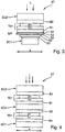
- FIG. 4 a solar cell stack ST with three subcells SC1-SC3 and with two tunnel diodes TD1 according to the invention is shown. The following are just the differences from the illustration of FIG. 1 explained.
- All three sub-cells SC1-SC3 of the solar cell stack ST are lattice-matched to one another.
- a further intermediate layer sequence with a further first barrier layer B1 and a further tunnel diode TD1 and a further second barrier layer B2 is arranged.
- a third subcell SC3 is arranged.
- the incidence of light L takes place through the third subcell SC3.
- FIG. 5 1 shows a solar cell stack ST with four subcells SC1-SC4 and with two tunnel diodes TD1 according to the invention and a non-strained tunnel diode TDLM.
- the following are just the differences from the illustration of FIG. 4 explained.
- a fourth subcell SC4 is arranged.
- the incidence of light L takes place through the fourth subcell SC4.
- All four sub-cells SC1-SC4 of the solar cell stack ST are lattice-matched to one another.
- an unstrained tunnel diode TDLM is arranged between the second subcell SC2 and the third subcell SC3 between the second subcell SC2 and the third subcell SC3. Both degenerate layers of the tunnel diode TDLM are lattice-matched to the sub-cells SC1-SC4.
- two strained tunnel diodes TD1 are installed, also adds the caused by the two p + layers tensile strain.
- the course of the height of the lattice constant is also shown to the right next to the representation of the solar cell stack ST. It turns out that in the case of the two strained tunnel diodes TD1 there is in each case a tensile strain, so that the solar cell stack as a whole has at least a first approximation the sum of the tensile strain from the two strained tunnel diodes TD1.
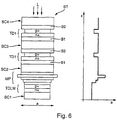
- FIG. 2 shows a solar cell stack ST with four subcells SC1-SC4 and with two tunnel diodes TD1 according to the invention and one metamorphic buffer MP and a non-strained tunnel diode TDLM.
- the following are just the differences from the illustration of FIG. 3 and the FIG. 5 explained.
- the three subcells SC2-SC4 of the solar cell stack ST are lattice-matched to one another.
- the tunnel diode TDLM of the prior art is arranged between the first subcell SC1 and the metamorphic buffer MP1.
- a first strained tunnel diode TD1 and between the third subcell SC3 and the fourth subcell SC4 a further second strained tunnel diode TD1 is arranged.
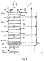
- FIG. 7 a solar cell stack ST with five subcells SC1-SC5 and with three tunnel diodes TD1 according to the invention and a metamorphic buffer MP and a non-strained tunnel diode TDLM is illustrated. The following are just the differences from the illustration of FIG. 6 explained.
- the second subcell are SC2 up to and including the fifth subcell SC5 of the solar cell stack ST lattice matched to each other.
- TD1 is arranged between the fourth subcell SC4 and the fifth subcell SC5.
- the representation of the profile of the lattice constant a to the right of the stack shows that the compressive stress caused by the large lattice constant of the fourth layer S4 of the metamorphic buffer MP, without additional layers, is at least partially or completely by means of the three tensile-stressed tunnel diode layers of TD1 compensate.
- a first full-area metal contact connection layer M1 is formed on the underside of the solar cell stack ST.
- an antireflection film AR is applied by means of a masking process.
- the antireflection layer is interrupted for the formation of a finger-like interconnect structure.
- the conductor track structure comprises an electrically conductive termination layer CP arranged on the upper side of the fifth subcell SC5 and a second metal contact connection layer M2 formed above the attachment layer.
- the layer thicknesses of the respective subcell can be reduced by at least 30% compared to a subcell without a Bragg mirror.
Landscapes
- Photovoltaic Devices (AREA)
- Life Sciences & Earth Sciences (AREA)
- Engineering & Computer Science (AREA)
- Sustainable Energy (AREA)
Applications Claiming Priority (1)
| Application Number | Priority Date | Filing Date | Title |
|---|---|---|---|
| DE102017005950.0A DE102017005950A1 (de) | 2017-06-21 | 2017-06-21 | Solarzellenstapel |
Publications (2)
| Publication Number | Publication Date |
|---|---|
| EP3419060A1 true EP3419060A1 (fr) | 2018-12-26 |
| EP3419060B1 EP3419060B1 (fr) | 2019-06-12 |
Family
ID=62712705
Family Applications (1)
| Application Number | Title | Priority Date | Filing Date |
|---|---|---|---|
| EP18000531.6A Active EP3419060B1 (fr) | 2017-06-21 | 2018-06-18 | Empilement de cellules solaires |
Country Status (5)
| Country | Link |
|---|---|
| US (1) | US10896986B2 (fr) |
| EP (1) | EP3419060B1 (fr) |
| CN (1) | CN109103293B (fr) |
| DE (1) | DE102017005950A1 (fr) |
| ES (1) | ES2744857T3 (fr) |
Cited By (1)
| Publication number | Priority date | Publication date | Assignee | Title |
|---|---|---|---|---|
| EP3712965A1 (fr) * | 2019-03-22 | 2020-09-23 | AZUR SPACE Solar Power GmbH | Cellule solaire de concentrateur terrestre, métamorphique droit, monolithique et en forme d'empilement |
Families Citing this family (7)
| Publication number | Priority date | Publication date | Assignee | Title |
|---|---|---|---|---|
| US20230207717A1 (en) * | 2016-10-14 | 2023-06-29 | Solaero Technologies Corp. | Multijunction metamorphic solar cells |
| US20220190181A1 (en) * | 2017-08-18 | 2022-06-16 | Solaero Technologies Corp. | Multijunction metamorphic solar cells |
| RU2701873C1 (ru) * | 2019-04-15 | 2019-10-02 | Федеральное государственное бюджетное учреждение науки Физико-технический институт им. А.Ф. Иоффе Российской академии наук | Полупроводниковая структура многопереходного фотопреобразователя |
| DE102020001185A1 (de) | 2020-02-25 | 2021-08-26 | Azur Space Solar Power Gmbh | Stapelförmige monolithische aufrecht-metamorphe lll-V-Mehrfachsolarzelle |
| CN113540281B (zh) * | 2020-04-13 | 2024-03-29 | 隆基绿能科技股份有限公司 | 叠层光伏器件 |
| EP3937259A1 (fr) * | 2020-07-10 | 2022-01-12 | AZUR SPACE Solar Power GmbH | Cellule solaire multiple métamorphique monolithique |
| EP3965169B1 (fr) * | 2020-09-07 | 2023-02-15 | AZUR SPACE Solar Power GmbH | Cellule solaire multiple monolithique empilée |
Citations (2)
| Publication number | Priority date | Publication date | Assignee | Title |
|---|---|---|---|---|
| JPH0964386A (ja) * | 1995-08-18 | 1997-03-07 | Japan Energy Corp | 多接合太陽電池 |
| EP2251912A1 (fr) * | 2009-05-11 | 2010-11-17 | Fraunhofer-Gesellschaft zur Förderung der angewandten Forschung e.V. | Diodes tunnel composées de couches semi-conductrices de liaison compensées en tension |
Family Cites Families (14)
| Publication number | Priority date | Publication date | Assignee | Title |
|---|---|---|---|---|
| US6933539B1 (en) * | 2004-05-17 | 2005-08-23 | Corning Incorporated | Tunnel junctions for long-wavelength VCSELs |
| IT1394221B1 (it) | 2009-05-15 | 2012-06-01 | Colbachini Spa | Tubo flessibile di tipo perfezionato per il trasporto di materiali fluidi e di corrente elettrica. |
| US11417788B2 (en) * | 2010-11-19 | 2022-08-16 | The Boeing Company | Type-II high bandgap tunnel junctions of InP lattice constant for multijunction solar cells |
| CN102184980B (zh) * | 2011-04-02 | 2013-10-30 | 中国科学院苏州纳米技术与纳米仿生研究所 | 基于晶片键合的三结太阳能电池及其制备方法 |
| CN102339889A (zh) * | 2011-09-14 | 2012-02-01 | 中国科学院苏州纳米技术与纳米仿生研究所 | 双结串行式InGaAs/InGaAsP双端太阳电池及其制作方法 |
| DE102012004734A1 (de) * | 2012-03-08 | 2013-09-12 | Fraunhofer-Gesellschaft zur Förderung der angewandten Forschung e.V. | Mehrfachsolarzelle und deren Verwendung |
| US20140196773A1 (en) * | 2013-01-11 | 2014-07-17 | International Business Machines Corporation | Multi-junction iii-v solar cell |
| JP6550691B2 (ja) * | 2013-07-30 | 2019-07-31 | 株式会社リコー | 化合物半導体太陽電池 |
| ES2749215T3 (es) * | 2014-03-13 | 2020-03-19 | Azur Space Solar Power Gmbh | Célula solar múltiple |
| EP2947702B1 (fr) * | 2014-05-21 | 2019-03-20 | AZUR SPACE Solar Power GmbH | Empilement de cellules solaires |
| JP6582591B2 (ja) * | 2014-07-11 | 2019-10-02 | 株式会社リコー | 化合物半導体太陽電池、及び、化合物半導体太陽電池の製造方法 |
| CN104201229B (zh) * | 2014-09-18 | 2016-09-28 | 厦门市三安光电科技有限公司 | 多结太阳能电池及其制备方法 |
| US20170084771A1 (en) * | 2015-09-21 | 2017-03-23 | The Boeing Company | Antimonide-based high bandgap tunnel junction for semiconductor devices |
| DE102015016047A1 (de) * | 2015-12-10 | 2017-06-14 | Azur Space Solar Power Gmbh | Mehrfach-Solarzelle |
-
2017
- 2017-06-21 DE DE102017005950.0A patent/DE102017005950A1/de not_active Withdrawn
-
2018
- 2018-06-18 EP EP18000531.6A patent/EP3419060B1/fr active Active
- 2018-06-18 ES ES18000531T patent/ES2744857T3/es active Active
- 2018-06-21 CN CN201810642075.8A patent/CN109103293B/zh active Active
- 2018-06-21 US US16/014,554 patent/US10896986B2/en active Active
Patent Citations (2)
| Publication number | Priority date | Publication date | Assignee | Title |
|---|---|---|---|---|
| JPH0964386A (ja) * | 1995-08-18 | 1997-03-07 | Japan Energy Corp | 多接合太陽電池 |
| EP2251912A1 (fr) * | 2009-05-11 | 2010-11-17 | Fraunhofer-Gesellschaft zur Förderung der angewandten Forschung e.V. | Diodes tunnel composées de couches semi-conductrices de liaison compensées en tension |
Non-Patent Citations (2)
| Title |
|---|
| ANDREAS W. BETT ET AL: "Highest efficiency multi-junction solar cell for terrestrial and space applications", PROCEEDINGS OF THE 24TH EUROPEAN PHOTOVOLTAIC SOLAR ENERGY CONFERENCE AND EXHIBITION, 21 September 2009 (2009-09-21) - 25 September 2009 (2009-09-25), Hamburg-GERMANY, pages 1 - 6, XP040529663, ISBN: 978-3-936338-25-6 * |
| W. GUTER ET AL: "Investigation and development of III-V-triple-junction concentrator solar cells", PROCEEDINGS OF THE 22ND EUROPEAN PHOTOVOLTAIC SOLAR ENERGY CONFERENCE, 3 September 2007 (2007-09-03) - 7 September 2007 (2007-09-07), Milan-ITALY, pages 122 - 125, XP040512959, ISBN: 978-3-936338-22-5 * |
Cited By (2)
| Publication number | Priority date | Publication date | Assignee | Title |
|---|---|---|---|---|
| EP3712965A1 (fr) * | 2019-03-22 | 2020-09-23 | AZUR SPACE Solar Power GmbH | Cellule solaire de concentrateur terrestre, métamorphique droit, monolithique et en forme d'empilement |
| US11984523B2 (en) | 2019-03-22 | 2024-05-14 | Azur Space Solar Power Gmbh | Stacked, monolithic, upright metamorphic, terrestrial concentrator solar cell |
Also Published As
| Publication number | Publication date |
|---|---|
| DE102017005950A1 (de) | 2018-12-27 |
| US10896986B2 (en) | 2021-01-19 |
| US20180374973A1 (en) | 2018-12-27 |
| CN109103293B (zh) | 2021-12-10 |
| CN109103293A (zh) | 2018-12-28 |
| EP3419060B1 (fr) | 2019-06-12 |
| ES2744857T3 (es) | 2020-02-26 |
Similar Documents
| Publication | Publication Date | Title |
|---|---|---|
| EP3419060B1 (fr) | Empilement de cellules solaires | |
| DE102008034711B4 (de) | Invertierte metamorphe Multijunction-Solarzelle mit Barrierenschicht und Verfahren zur Herstellung | |
| EP2430672B1 (fr) | Diodes tunnel composées de couches semi-conductrices de liaison compensées en tension | |
| EP2919276B1 (fr) | Cellule solaire à jonctions multiples | |
| EP3179521A1 (fr) | Cellule solaire à jonctions multiples | |
| DE102014000156A1 (de) | Mehrfachsolarzelle mit einer einen niedrigen Bandabstand aufweisenden Absorptionsschicht in der Mittelzelle | |
| DE2607005C2 (de) | Integrierte Tandem-Solarzelle | |
| DE202012104415U1 (de) | Mehrfachübergangs-Solarzellen hohen Wirkungsgrades | |
| DE102015016822B4 (de) | Stapelförmige Mehrfach-Solarzelle | |
| WO2018134016A1 (fr) | Cellule solaire multiple avec sous-cellule au germanium au dos et son utilisation | |
| DE102018203509B4 (de) | Vierfach-Solarzelle für Raumanwendungen | |
| EP3012874B1 (fr) | Cellule solaire à jonctions multiples intégrée en forme de pile | |
| EP3018718B1 (fr) | Piles de cellules solaires | |
| EP3667742A1 (fr) | Cellule solaire à multijonction, métamorphique verticale, monolithique, empilée | |
| DE102010010880A1 (de) | Multijunction-Solarzellen basierend auf Gruppe-IV/III-V Hybrid-Halbleiterverbindungen | |
| DE102016116192B3 (de) | Photovoltaikmodul mit integriert serienverschalteten Stapel-Solarzellen und Verfahren zu seiner Herstellung | |
| EP3965168B1 (fr) | Cellule solaire multiple monolithique empilée | |
| EP3712965A1 (fr) | Cellule solaire de concentrateur terrestre, métamorphique droit, monolithique et en forme d'empilement | |
| DE102018009850B4 (de) | Stapelförmige Mehrfachsolarzelle | |
| DE102016005640A1 (de) | Invertierte Mehrfach-Solarzelle | |
| EP3937259A1 (fr) | Cellule solaire multiple métamorphique monolithique | |
| EP3937260A1 (fr) | Cellule solaire multiple métamorphique monolithique | |
| EP3965169B1 (fr) | Cellule solaire multiple monolithique empilée | |
| EP3799136B1 (fr) | Cellule solaire monolithique à multi-jonctions comportant exactement quatre sous-cellules | |
| DE102020000549B4 (de) | Stapelförmiges photonisches III-V-Halbleiterbauelement |
Legal Events
| Date | Code | Title | Description |
|---|---|---|---|
| PUAI | Public reference made under article 153(3) epc to a published international application that has entered the european phase |
Free format text: ORIGINAL CODE: 0009012 |
|
| STAA | Information on the status of an ep patent application or granted ep patent |
Free format text: STATUS: THE APPLICATION HAS BEEN PUBLISHED |
|
| STAA | Information on the status of an ep patent application or granted ep patent |
Free format text: STATUS: REQUEST FOR EXAMINATION WAS MADE |
|
| AK | Designated contracting states |
Kind code of ref document: A1 Designated state(s): AL AT BE BG CH CY CZ DE DK EE ES FI FR GB GR HR HU IE IS IT LI LT LU LV MC MK MT NL NO PL PT RO RS SE SI SK SM TR |
|
| AX | Request for extension of the european patent |
Extension state: BA ME |
|
| 17P | Request for examination filed |
Effective date: 20181210 |
|
| RBV | Designated contracting states (corrected) |
Designated state(s): AL AT BE BG CH CY CZ DE DK EE ES FI FR GB GR HR HU IE IS IT LI LT LU LV MC MK MT NL NO PL PT RO RS SE SI SK SM TR |
|
| GRAP | Despatch of communication of intention to grant a patent |
Free format text: ORIGINAL CODE: EPIDOSNIGR1 |
|
| RIC1 | Information provided on ipc code assigned before grant |
Ipc: H01L 31/0304 20060101ALI20190124BHEP Ipc: H01L 31/0687 20120101AFI20190124BHEP |
|
| STAA | Information on the status of an ep patent application or granted ep patent |
Free format text: STATUS: GRANT OF PATENT IS INTENDED |
|
| INTG | Intention to grant announced |
Effective date: 20190228 |
|
| GRAS | Grant fee paid |
Free format text: ORIGINAL CODE: EPIDOSNIGR3 |
|
| GRAA | (expected) grant |
Free format text: ORIGINAL CODE: 0009210 |
|
| STAA | Information on the status of an ep patent application or granted ep patent |
Free format text: STATUS: THE PATENT HAS BEEN GRANTED |
|
| AK | Designated contracting states |
Kind code of ref document: B1 Designated state(s): AL AT BE BG CH CY CZ DE DK EE ES FI FR GB GR HR HU IE IS IT LI LT LU LV MC MK MT NL NO PL PT RO RS SE SI SK SM TR |
|
| REG | Reference to a national code |
Ref country code: GB Ref legal event code: FG4D Free format text: NOT ENGLISH |
|
| REG | Reference to a national code |
Ref country code: CH Ref legal event code: EP |
|
| REG | Reference to a national code |
Ref country code: AT Ref legal event code: REF Ref document number: 1143719 Country of ref document: AT Kind code of ref document: T Effective date: 20190615 |
|
| REG | Reference to a national code |
Ref country code: DE Ref legal event code: R096 Ref document number: 502018000043 Country of ref document: DE |
|
| REG | Reference to a national code |
Ref country code: IE Ref legal event code: FG4D Free format text: LANGUAGE OF EP DOCUMENT: GERMAN |
|
| REG | Reference to a national code |
Ref country code: NL Ref legal event code: FP |
|
| REG | Reference to a national code |
Ref country code: LT Ref legal event code: MG4D |
|
| PG25 | Lapsed in a contracting state [announced via postgrant information from national office to epo] |
Ref country code: HR Free format text: LAPSE BECAUSE OF FAILURE TO SUBMIT A TRANSLATION OF THE DESCRIPTION OR TO PAY THE FEE WITHIN THE PRESCRIBED TIME-LIMIT Effective date: 20190612 Ref country code: SE Free format text: LAPSE BECAUSE OF FAILURE TO SUBMIT A TRANSLATION OF THE DESCRIPTION OR TO PAY THE FEE WITHIN THE PRESCRIBED TIME-LIMIT Effective date: 20190612 Ref country code: AL Free format text: LAPSE BECAUSE OF FAILURE TO SUBMIT A TRANSLATION OF THE DESCRIPTION OR TO PAY THE FEE WITHIN THE PRESCRIBED TIME-LIMIT Effective date: 20190612 Ref country code: FI Free format text: LAPSE BECAUSE OF FAILURE TO SUBMIT A TRANSLATION OF THE DESCRIPTION OR TO PAY THE FEE WITHIN THE PRESCRIBED TIME-LIMIT Effective date: 20190612 Ref country code: NO Free format text: LAPSE BECAUSE OF FAILURE TO SUBMIT A TRANSLATION OF THE DESCRIPTION OR TO PAY THE FEE WITHIN THE PRESCRIBED TIME-LIMIT Effective date: 20190912 Ref country code: LT Free format text: LAPSE BECAUSE OF FAILURE TO SUBMIT A TRANSLATION OF THE DESCRIPTION OR TO PAY THE FEE WITHIN THE PRESCRIBED TIME-LIMIT Effective date: 20190612 |
|
| PG25 | Lapsed in a contracting state [announced via postgrant information from national office to epo] |
Ref country code: RS Free format text: LAPSE BECAUSE OF FAILURE TO SUBMIT A TRANSLATION OF THE DESCRIPTION OR TO PAY THE FEE WITHIN THE PRESCRIBED TIME-LIMIT Effective date: 20190612 Ref country code: BG Free format text: LAPSE BECAUSE OF FAILURE TO SUBMIT A TRANSLATION OF THE DESCRIPTION OR TO PAY THE FEE WITHIN THE PRESCRIBED TIME-LIMIT Effective date: 20190912 Ref country code: LV Free format text: LAPSE BECAUSE OF FAILURE TO SUBMIT A TRANSLATION OF THE DESCRIPTION OR TO PAY THE FEE WITHIN THE PRESCRIBED TIME-LIMIT Effective date: 20190612 Ref country code: GR Free format text: LAPSE BECAUSE OF FAILURE TO SUBMIT A TRANSLATION OF THE DESCRIPTION OR TO PAY THE FEE WITHIN THE PRESCRIBED TIME-LIMIT Effective date: 20190913 |
|
| PG25 | Lapsed in a contracting state [announced via postgrant information from national office to epo] |
Ref country code: EE Free format text: LAPSE BECAUSE OF FAILURE TO SUBMIT A TRANSLATION OF THE DESCRIPTION OR TO PAY THE FEE WITHIN THE PRESCRIBED TIME-LIMIT Effective date: 20190612 Ref country code: SK Free format text: LAPSE BECAUSE OF FAILURE TO SUBMIT A TRANSLATION OF THE DESCRIPTION OR TO PAY THE FEE WITHIN THE PRESCRIBED TIME-LIMIT Effective date: 20190612 Ref country code: CZ Free format text: LAPSE BECAUSE OF FAILURE TO SUBMIT A TRANSLATION OF THE DESCRIPTION OR TO PAY THE FEE WITHIN THE PRESCRIBED TIME-LIMIT Effective date: 20190612 Ref country code: RO Free format text: LAPSE BECAUSE OF FAILURE TO SUBMIT A TRANSLATION OF THE DESCRIPTION OR TO PAY THE FEE WITHIN THE PRESCRIBED TIME-LIMIT Effective date: 20190612 Ref country code: PT Free format text: LAPSE BECAUSE OF FAILURE TO SUBMIT A TRANSLATION OF THE DESCRIPTION OR TO PAY THE FEE WITHIN THE PRESCRIBED TIME-LIMIT Effective date: 20191014 |
|
| REG | Reference to a national code |
Ref country code: ES Ref legal event code: FG2A Ref document number: 2744857 Country of ref document: ES Kind code of ref document: T3 Effective date: 20200226 |
|
| PG25 | Lapsed in a contracting state [announced via postgrant information from national office to epo] |
Ref country code: SM Free format text: LAPSE BECAUSE OF FAILURE TO SUBMIT A TRANSLATION OF THE DESCRIPTION OR TO PAY THE FEE WITHIN THE PRESCRIBED TIME-LIMIT Effective date: 20190612 Ref country code: IS Free format text: LAPSE BECAUSE OF FAILURE TO SUBMIT A TRANSLATION OF THE DESCRIPTION OR TO PAY THE FEE WITHIN THE PRESCRIBED TIME-LIMIT Effective date: 20191012 |
|
| REG | Reference to a national code |
Ref country code: DE Ref legal event code: R097 Ref document number: 502018000043 Country of ref document: DE |
|
| PG25 | Lapsed in a contracting state [announced via postgrant information from national office to epo] |
Ref country code: MC Free format text: LAPSE BECAUSE OF FAILURE TO SUBMIT A TRANSLATION OF THE DESCRIPTION OR TO PAY THE FEE WITHIN THE PRESCRIBED TIME-LIMIT Effective date: 20190612 Ref country code: TR Free format text: LAPSE BECAUSE OF FAILURE TO SUBMIT A TRANSLATION OF THE DESCRIPTION OR TO PAY THE FEE WITHIN THE PRESCRIBED TIME-LIMIT Effective date: 20190612 |
|
| PLBE | No opposition filed within time limit |
Free format text: ORIGINAL CODE: 0009261 |
|
| STAA | Information on the status of an ep patent application or granted ep patent |
Free format text: STATUS: NO OPPOSITION FILED WITHIN TIME LIMIT |
|
| PG25 | Lapsed in a contracting state [announced via postgrant information from national office to epo] |
Ref country code: PL Free format text: LAPSE BECAUSE OF FAILURE TO SUBMIT A TRANSLATION OF THE DESCRIPTION OR TO PAY THE FEE WITHIN THE PRESCRIBED TIME-LIMIT Effective date: 20190612 Ref country code: DK Free format text: LAPSE BECAUSE OF FAILURE TO SUBMIT A TRANSLATION OF THE DESCRIPTION OR TO PAY THE FEE WITHIN THE PRESCRIBED TIME-LIMIT Effective date: 20190612 |
|
| 26N | No opposition filed |
Effective date: 20200313 |
|
| PG25 | Lapsed in a contracting state [announced via postgrant information from national office to epo] |
Ref country code: IS Free format text: LAPSE BECAUSE OF FAILURE TO SUBMIT A TRANSLATION OF THE DESCRIPTION OR TO PAY THE FEE WITHIN THE PRESCRIBED TIME-LIMIT Effective date: 20200224 |
|
| PG2D | Information on lapse in contracting state deleted |
Ref country code: IS |
|
| PG25 | Lapsed in a contracting state [announced via postgrant information from national office to epo] |
Ref country code: LU Free format text: LAPSE BECAUSE OF NON-PAYMENT OF DUE FEES Effective date: 20200618 |
|
| PG25 | Lapsed in a contracting state [announced via postgrant information from national office to epo] |
Ref country code: IE Free format text: LAPSE BECAUSE OF NON-PAYMENT OF DUE FEES Effective date: 20200618 |
|
| PG25 | Lapsed in a contracting state [announced via postgrant information from national office to epo] |
Ref country code: HU Free format text: LAPSE BECAUSE OF FAILURE TO SUBMIT A TRANSLATION OF THE DESCRIPTION OR TO PAY THE FEE WITHIN THE PRESCRIBED TIME-LIMIT; INVALID AB INITIO Effective date: 20180618 |
|
| REG | Reference to a national code |
Ref country code: CH Ref legal event code: PL |
|
| PG25 | Lapsed in a contracting state [announced via postgrant information from national office to epo] |
Ref country code: LI Free format text: LAPSE BECAUSE OF NON-PAYMENT OF DUE FEES Effective date: 20210630 Ref country code: CH Free format text: LAPSE BECAUSE OF NON-PAYMENT OF DUE FEES Effective date: 20210630 |
|
| PG25 | Lapsed in a contracting state [announced via postgrant information from national office to epo] |
Ref country code: MT Free format text: LAPSE BECAUSE OF FAILURE TO SUBMIT A TRANSLATION OF THE DESCRIPTION OR TO PAY THE FEE WITHIN THE PRESCRIBED TIME-LIMIT Effective date: 20190612 Ref country code: CY Free format text: LAPSE BECAUSE OF FAILURE TO SUBMIT A TRANSLATION OF THE DESCRIPTION OR TO PAY THE FEE WITHIN THE PRESCRIBED TIME-LIMIT Effective date: 20190612 |
|
| PG25 | Lapsed in a contracting state [announced via postgrant information from national office to epo] |
Ref country code: MK Free format text: LAPSE BECAUSE OF FAILURE TO SUBMIT A TRANSLATION OF THE DESCRIPTION OR TO PAY THE FEE WITHIN THE PRESCRIBED TIME-LIMIT Effective date: 20190612 |
|
| PG25 | Lapsed in a contracting state [announced via postgrant information from national office to epo] |
Ref country code: SI Free format text: LAPSE BECAUSE OF FAILURE TO SUBMIT A TRANSLATION OF THE DESCRIPTION OR TO PAY THE FEE WITHIN THE PRESCRIBED TIME-LIMIT Effective date: 20190612 |
|
| P01 | Opt-out of the competence of the unified patent court (upc) registered |
Free format text: CASE NUMBER: APP_40037/2024 Effective date: 20240704 |
|
| REG | Reference to a national code |
Ref country code: AT Ref legal event code: MM01 Ref document number: 1143719 Country of ref document: AT Kind code of ref document: T Effective date: 20230618 |
|
| PG25 | Lapsed in a contracting state [announced via postgrant information from national office to epo] |
Ref country code: AT Free format text: LAPSE BECAUSE OF NON-PAYMENT OF DUE FEES Effective date: 20230618 |
|
| PG25 | Lapsed in a contracting state [announced via postgrant information from national office to epo] |
Ref country code: AT Free format text: LAPSE BECAUSE OF NON-PAYMENT OF DUE FEES Effective date: 20230618 |
|
| REG | Reference to a national code |
Ref country code: DE Ref legal event code: R079 Ref document number: 502018000043 Country of ref document: DE Free format text: PREVIOUS MAIN CLASS: H01L0031068700 Ipc: H10F0010142000 |
|
| PGFP | Annual fee paid to national office [announced via postgrant information from national office to epo] |
Ref country code: DE Payment date: 20250618 Year of fee payment: 8 |
|
| PGFP | Annual fee paid to national office [announced via postgrant information from national office to epo] |
Ref country code: GB Payment date: 20250618 Year of fee payment: 8 |
|
| PGFP | Annual fee paid to national office [announced via postgrant information from national office to epo] |
Ref country code: NL Payment date: 20250618 Year of fee payment: 8 Ref country code: BE Payment date: 20250618 Year of fee payment: 8 |
|
| PGFP | Annual fee paid to national office [announced via postgrant information from national office to epo] |
Ref country code: FR Payment date: 20250625 Year of fee payment: 8 |
|
| PGFP | Annual fee paid to national office [announced via postgrant information from national office to epo] |
Ref country code: ES Payment date: 20250728 Year of fee payment: 8 |
|
| PGFP | Annual fee paid to national office [announced via postgrant information from national office to epo] |
Ref country code: IT Payment date: 20250624 Year of fee payment: 8 |
|
| PGFP | Annual fee paid to national office [announced via postgrant information from national office to epo] |
Ref country code: AT Payment date: 20260410 Year of fee payment: 5 |