EP2432034B1 - Bispektraler mehrschichtiger Detektor mit Fotodioden, und Herstellungsverfahren für einen solchen Detektor - Google Patents
Bispektraler mehrschichtiger Detektor mit Fotodioden, und Herstellungsverfahren für einen solchen Detektor Download PDFInfo
- Publication number
- EP2432034B1 EP2432034B1 EP11306126.1A EP11306126A EP2432034B1 EP 2432034 B1 EP2432034 B1 EP 2432034B1 EP 11306126 A EP11306126 A EP 11306126A EP 2432034 B1 EP2432034 B1 EP 2432034B1
- Authority
- EP
- European Patent Office
- Prior art keywords
- layer
- conductivity type
- semiconductor
- upper layer
- mercury
- Prior art date
- Legal status (The legal status is an assumption and is not a legal conclusion. Google has not performed a legal analysis and makes no representation as to the accuracy of the status listed.)
- Active
Links
Images




Classifications
-
- H—ELECTRICITY
- H10—SEMICONDUCTOR DEVICES; ELECTRIC SOLID-STATE DEVICES NOT OTHERWISE PROVIDED FOR
- H10F—INORGANIC SEMICONDUCTOR DEVICES SENSITIVE TO INFRARED RADIATION, LIGHT, ELECTROMAGNETIC RADIATION OF SHORTER WAVELENGTH OR CORPUSCULAR RADIATION
- H10F71/00—Manufacture or treatment of devices covered by this subclass
- H10F71/125—The active layers comprising only Group II-VI materials, e.g. CdS, ZnS or CdTe
- H10F71/1253—The active layers comprising only Group II-VI materials, e.g. CdS, ZnS or CdTe comprising at least three elements, e.g. HgCdTe
-
- H—ELECTRICITY
- H10—SEMICONDUCTOR DEVICES; ELECTRIC SOLID-STATE DEVICES NOT OTHERWISE PROVIDED FOR
- H10F—INORGANIC SEMICONDUCTOR DEVICES SENSITIVE TO INFRARED RADIATION, LIGHT, ELECTROMAGNETIC RADIATION OF SHORTER WAVELENGTH OR CORPUSCULAR RADIATION
- H10F30/00—Individual radiation-sensitive semiconductor devices in which radiation controls the flow of current through the devices, e.g. photodetectors
- H10F30/20—Individual radiation-sensitive semiconductor devices in which radiation controls the flow of current through the devices, e.g. photodetectors the devices having potential barriers, e.g. phototransistors
- H10F30/21—Individual radiation-sensitive semiconductor devices in which radiation controls the flow of current through the devices, e.g. photodetectors the devices having potential barriers, e.g. phototransistors the devices being sensitive to infrared, visible or ultraviolet radiation
- H10F30/288—Individual radiation-sensitive semiconductor devices in which radiation controls the flow of current through the devices, e.g. photodetectors the devices having potential barriers, e.g. phototransistors the devices being sensitive to infrared, visible or ultraviolet radiation the devices being sensitive to multiple wavelengths, e.g. multi-spectrum radiation detection devices
-
- H—ELECTRICITY
- H10—SEMICONDUCTOR DEVICES; ELECTRIC SOLID-STATE DEVICES NOT OTHERWISE PROVIDED FOR
- H10F—INORGANIC SEMICONDUCTOR DEVICES SENSITIVE TO INFRARED RADIATION, LIGHT, ELECTROMAGNETIC RADIATION OF SHORTER WAVELENGTH OR CORPUSCULAR RADIATION
- H10F39/00—Integrated devices, or assemblies of multiple devices, comprising at least one element covered by group H10F30/00, e.g. radiation detectors comprising photodiode arrays
- H10F39/011—Manufacture or treatment of image sensors covered by group H10F39/12
- H10F39/022—Manufacture or treatment of image sensors covered by group H10F39/12 of image sensors having active layers comprising only Group II-VI materials, e.g. CdS, ZnS or CdTe
-
- H—ELECTRICITY
- H10—SEMICONDUCTOR DEVICES; ELECTRIC SOLID-STATE DEVICES NOT OTHERWISE PROVIDED FOR
- H10F—INORGANIC SEMICONDUCTOR DEVICES SENSITIVE TO INFRARED RADIATION, LIGHT, ELECTROMAGNETIC RADIATION OF SHORTER WAVELENGTH OR CORPUSCULAR RADIATION
- H10F39/00—Integrated devices, or assemblies of multiple devices, comprising at least one element covered by group H10F30/00, e.g. radiation detectors comprising photodiode arrays
- H10F39/10—Integrated devices
- H10F39/12—Image sensors
- H10F39/18—Complementary metal-oxide-semiconductor [CMOS] image sensors; Photodiode array image sensors
- H10F39/184—Infrared image sensors
- H10F39/1847—Multispectral infrared image sensors having a stacked structure, e.g. NPN, NPNPN or multiple quantum well [MQW] structures
-
- H—ELECTRICITY
- H10—SEMICONDUCTOR DEVICES; ELECTRIC SOLID-STATE DEVICES NOT OTHERWISE PROVIDED FOR
- H10F—INORGANIC SEMICONDUCTOR DEVICES SENSITIVE TO INFRARED RADIATION, LIGHT, ELECTROMAGNETIC RADIATION OF SHORTER WAVELENGTH OR CORPUSCULAR RADIATION
- H10F39/00—Integrated devices, or assemblies of multiple devices, comprising at least one element covered by group H10F30/00, e.g. radiation detectors comprising photodiode arrays
- H10F39/80—Constructional details of image sensors
- H10F39/813—Electronic components shared by multiple pixels, e.g. one amplifier shared by two pixels
Definitions
- the invention relates to the field of bi-spectral detection by means of two absorption layers of the same stack, and in which PN junctions are formed.
- a preferred bispectral detector due to its high filling rate and its temporal coherence comprises a stack of several absorption semiconductor layers of different frequency ranges of electromagnetic radiation, isolated from each other, and in which are formed PN junctions for the collection of charge carriers created by the absorption of incident radiation.
- Such a detector is for example described in the documents US 6,034,407 and "Status of HgCdTe bicolor and dual-band infrared array at LETI" by Destefanis, Journal of Electronic Materials 36 (8), p.1031, (2007) ). These first two references concern the CdHgTe material.
- Kim A Three Wavelength Infrared Focal Plane Array Detector Element", IEEEPhotonicsTechLett 6 (2) p235 (1994) ).
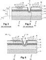
- figure 1 is a top view of this detector, shown here in the form of a two-pixel two pixel detector by three pixels, the figure 2 is a sectional view along the axis AA shown in FIG. figure 1 , and the figure 3 is a cadmium composition x profile of the various alloys of cadmium, mercury and tellurium (Cd x Hg 1-x Te) forming the stack of the detector.
- N-type 20 are also formed in the upper layer 18, by ion implanting boron, for example. This ion implantation step has the effect of converting intrinsic doping P type N type and thus form a matrix of PN junctions, and therefore photodiodes.
- Recesses 22 are further machined through the upper layer 18 and the intermediate layer 16 to the lower layer 14 to have access thereto.
- N-type semiconductor zones 24 are produced in the lower layer 14 by applying N doping by boron ion implantation, for example, to the portions of the lower layer 14 flush with the bottom of the recesses 22. A matrix of PN junctions , and hence of photodiodes, is thus formed in the lower layer 14.
- the semiconductor zones 20 and the semiconductor zones 24 respectively form detection matrices of L lines by C columns, with L and C respectively equal to 2 and 3 in the example illustrated, and the zone matrix 24 is shifted with respect to the zone matrix 20 so as to have a zone 24 at the center of a rectangle or a square made up of four zones 20.
- a passivation layer 26 (not shown in FIG. figure 1 for the sake of clarity of the drawings) carried out using a CdTe / ZnS bilayer is also deposited on the free face of the upper layer 18 and in the recesses 22.
- a metal contact recovery 28 is formed on the upper layer 18 above each zone 20 and enters the zone 20 for the collection of the charges contained therein.
- a metal contact recovery 30 is deposited in each recess 22 in the form of a layer covering the sides of the recess and enters the corresponding zone 24 for the collection of the charges contained in this zone.
- the resumption of contact 30 is prolonged on the upper face of the passivation layer 26 to facilitate the connection of the recovery 30 to external connections (not shown).
- an indium ball 32, 34 is formed on the portion of each contact resumption 28, 30 formed on the upper face of the passivation layer 26 for the hybridization of the stack on a read circuit (not shown ) by the so-called " flip chip " technique.
- the detector 10 just described is a backside illuminated sensor .
- the free face of the substrate 12 receives an electromagnetic radiation RE which penetrates the stack.
- the portion of the radiation RE, included in the first range of wavelengths, is absorbed by the lower layer 14, and the portion of the radiation RE, included in the second wavelength range, is absorbed by the upper layer 18 .
- a bias is or is not applied between a common contact device (not shown in figure 2 ) and the contact reversals 28, 30 in a manner known per se.
- the role of the intermediate layer 16 is to prevent charge carriers, created in one of the layers 14, 18, from diffusing into the other layer 14, 18, thus causing a phenomenon of crosstalk, or " cross- talk". talk ", detrimental to the quality of detection.
- This function is more commonly referred to as the "barrier" function.
- the quality of the barrier function of the intermediate layer 16 depends mainly on the difference existing between the value of the band gap, or " gap ", of the intermediate layer 16, and, on the one hand, that of the lower layer 14, and, on the other hand, that of the upper layer 18.
- the intermediate layer 16 thus forms a potential barrier separating the valence and conduction bands from the lower 14 and upper 18 layers , thus limiting the passage of the charge carriers of one layer to another.
- the gap value is determined mainly by the composition ( 1-x) in mercury, or equivalently by the composition of cadmium x.
- the figure 3 illustrates a typical profile of cadmium x compositions of the various layers of the stack with a composition x 16 of the intermediate layer 16, preferably at least 50%, to each composition x 14 , x 18 of the lower layers 14 and higher 18.
- the recesses 22 are necessary to access the lower layer 14, and thus allow the realization of the semiconductor zones 24, but also to be able to perform the contact resumption 30 for the collection of the charges of the zones 24.
- the walls thereof have many imperfections.
- the crystalline quality of the flanks of the hole can be degraded by etching with the consequence of a high recombination rate on the surface.
- the portions of the recesses 22 present in the upper layer 18 are sources of recombination for the charge carriers thereof, as well as sources of low frequency noise associated with this generation current for the PN junctions of this layer. 18.
- a solution usually adopted to overcome this problem is to distance the PN junctions of the upper layer 18 of the recesses 22.
- the fill rate of the pixel (or " fill factor ") is therefore reduced.
- Another solution is also to use techniques for machining the plasma recesses 22 and for repairing the flanks of the recesses by annealing. This solution would be ideally preferable, but requires perfect control of the etching process, which requires a heavy technological development.
- the object of the invention is to solve the problem posed by the imperfections of the recesses by proposing a detector and a detector manufacturing method, in which the recess portions included in the upper layer are rendered electrically invisible for this layer, while even these imperfections may still be present.
- the carriers generated by said surface visit the material around them by diffusion before recombining.
- the diffusion length is then defined by the average distance traveled by a minority carrier during its lifetime. This diffusion length decreases rapidly with doping (a fraction of a micrometer is conventionally obtained for a doping of 17 cm -3 ) .
- a passivation layer of Cd x Hg 1-x Te alloy which is initially of type P thanks to mercury vacancies and which then underwent an N-type doping conversion of a concentration greater than 10 17 , by ion implantation of boron, for example, and which has a thickness greater than 500 nanometers, effectively masks the recesses.
- This thickness can be chosen on the order of a hundred nanometers when the dopant N concentration is greater than or equal to 10 18 .
- the portion of each recess passing through the intermediate layer is separated from the latter by a semiconductor shield layer of the second conductivity type.
- the intermediate layer is made of an insulating material relative to the material of the upper and lower layers or of semiconductor material of the first conductivity type whose band gap is greater than three times that of each of the upper and lower layers. lower.
- the subject of the invention is also a method for manufacturing a bispectral detector as defined in claim 6.
- a doping of the second type of conductivity by ion implantation or ionic machining is carried out on the blanks of each recess. , at least on the portion of said sidewalls arranged in the upper layer.
- these doping techniques form on the surface of the elements to which they are applied a layer of high concentration of N dopant, or so-called "N +" layer, greater than 10 17 cm -3 , and this to a thickness sufficient to electrically mask the recesses.
- N + layer of high concentration of N dopant, or so-called "N +" layer, greater than 10 17 cm -3 , and this to a thickness sufficient to electrically mask the recesses.
- the doping of the second type of conductivity on the flanks of the recesses extends on the free face of the upper layer, so that the semiconductor zones of the second type are formed therein.
- the filling rate of the photodiodes is thus optimal.
- the semiconductor zones of the upper layer, as well as the electrical masking layers of the recesses are made in a single step, for example by applying appropriate masking during ion implantation.
- the second type of semiconductor zones in the upper layer are made so as not to be in contact with the semiconductor zones of the second type obtained at the end of the doping of the flanks. recesses.
- semiconductor elements of the second type in particular by ion implantation or ionic machining, connecting semiconductor zones of the second type obtained at the end of the doping of the flanks of the recesses. a common conductive element.
- the formation of the semiconductor elements makes it possible to put all the semiconductor zones of the recesses at the same potential.
- the detector 40 differs from the detector 10 Figures 1 to 3 by the shape of the N-type semiconductor zones, or "N-zones", implanted in the layers 14, 16, 18 of the stack. More particularly, after deposition of the passivation layer 26, N type doping is carried out by ion implantation of boron, for example, on portions of the upper face 42 of the stack through the passivation layer 26. This ion implantation is preferably carried out using an appropriate mask affixed to the upper face 42 and masking the latter, except for the portions to be implanted.
- the layers 12, 14, 16, the recesses 22, the covers of the contacts 28, 30 and the connectors 32, 34 are for their part for example made according to the method described in the document "Status of HgCdTe bicolor and dual-band infrared array at LETI” by Destefanis, JEM 36 (8), p.1031, 2007 .
- Each of the implanted portions comprises a recess 22 and extends over a portion of the upper layer 18 above which is formed the metal contact recovery 28, as illustrated in FIG. figure 4 .
- Spatially continuous volumes 44 of N areas are thus obtained.
- Each of these volumes 44 thus includes a recess 22, and constitutes at the same time a zone N for the formation of a PN junction in the upper layer 18 and an N zone, implanted at the bottom of the recess 22, for the formation of a PN junction in the lower layer 14.
- the figure 6 illustrates the spatial profile of the concentration of charge donors thus obtained by the ion implantation. This profile is taken along any axis perpendicular to the wall of a recess 22 included in the upper layer 18, and comprises the concentration of charge donors in a volume 44, as well as the concentration of charge donors in the upper layer 18 . concentrations are here plotted against the thickness depending on the relevant axis.
- a volume 44 is essentially divided into a first "N +" layer 46, of a thickness of about 100 nanometers and a dopant concentration N of about 18 , and a second layer "N-> 48, several hundred nanometers thick, for example 900 nm, and a lower concentration of N dopant. It is shown that the layer 46 is sufficient to electrically mask the walls of the recesses 22 to the charge carriers included in the upper layer 18.
- Such a profile is found substantially throughout the volume 44, only the portion “P” varying according to the upper layer 18, lower 14 or intermediate 16.
- the layer marked “N-” in the profile forms a PN junction with the zone noted “P” adjacent to the upper or lower layer.
- zones N can pass through the intermediate layer 16 because of the ion implantation which is carried out on all the flanks of the recesses 22. If we are not careful, the zones N thus formed may allow load carriers to pass between the upper layers 18 and lower 14, through the intermediate layer 16. A phenomenon of crosstalk can thus appear.
- the intermediate layer 16 could have been chosen so that the ion implantation carried out on the flanks of the recesses 22 does not create N-zones in the intermediate layer 16.
- the intermediate layer 16 could have consisted of a cadmium alloy and tellurium or an alloy of cadmium, zinc and tellurium. Not only, such an alloy is insulating vis-à-vis the P-type Cd x Hg 1-x Te alloys, and would achieve a barrier function of high quality, but in addition the ion implantation would not create in the intermediate layer 16 since the process of doping reversal occurs only through the presence of mercury in the alloy. Since there would be no continuity of the N zones between the upper and lower layers, the charge carriers could therefore not transit between these layers via the intermediate layer. The phenomenon of crosstalk would therefore be avoided.
- the technique used to form the upper layer 18 depends on the nature of the support on which it is made, and thus here of the intermediate layer 16.
- the aforementioned alloys are not the best suited to promote growth of the upper layer 16 by means of a molecular beam epitaxy, or " MJM " , which is usually the preferred technique for making Cd x Hg 1-x Te alloy layers.
- MJM molecular beam epitaxy
- the presence of mercury in the intermediate layer 16 has the effect that the subsequent ion implantation of the flanks of the recesses 22 forms in the layer 16 of the N zones, and therefore a possible passage for the charge carriers between the upper layers 18 and lower 16.
- the embodiment allows an optimization of the filling rate of the photodiodes created by the ion implantation.
- a degradation of the performances can be observed because the zones N in the upper layer 18 comprise vertical parts formed of the flanks of the recesses 22. Pinch zones in the PN junctions of the upper layer 18 can therefore occur, especially in places where the zone 44 forms an elbow.
- a nip in a PN junction has the effect of increasing the leakage currents therein, in particular by tunnel effect.
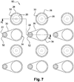
- a detector 50 not forming part of the present invention is illustrated in FIGS. figures 7 and 8 , and differs from the embodiment in that the N zones 20 of the upper layer, under the contact overlaps 28, are distinct from the N-type zones 52 formed on the flanks of the recesses 22, as illustrated in FIGS. figures 7 and 8 .
- the N 20 areas of the PN junctions of the upper layer 18 therefore do not include a pinching zone.
- the method of manufacturing the detector 50 thus differs from the method of manufacturing the detector 40 according to the embodiment by the geometry of the mask used during the ion implantation, this mask also masking a portion of the upper layer 18 around each recess 22 .
- the potential of the zones N, formed on the sides of the recesses 22 and included in the upper layer 18, is free to float because they are not connected to any fixed potential. These zones are electrically isolated from the zones of the lower layer 14 because of the barrier function performed by the intermediate layer 16, as explained above in connection with the choice of materials of the intermediate layer of the first embodiment, and are not elsewhere not connected to the N areas of the PN junctions of the upper layer 18 (which are brought to a potential for the collection of charges). In the absence of bias applied to the zone N on the side of the recesses 22, the PN junction will naturally be at its open circuit potential.
- the space charge area of this PN junction is likely to fluctuate over time, under the effect of fluctuations of various parameters (as for example fluctuation of the recombination current related to the surfaces of the recesses 22 ). Subsequently, these fluctuations of the N areas are also likely to modulate the current collected by the neighboring diodes. Such beats are potentially noise generators for neighboring PN junctions, mainly those of the upper layer 18.
- a detector 60 na not forming part of the present invention comprises N-type semiconductor elements 62, made for example by ion implantation in the upper layer 18, together with the production of the N 20 zones thereof. ci and N 52 areas on the flanks of the recesses 22.
- These elements 62 have the function of setting the potential of the portions of the zones N 52 included in the upper layer 18 to the same value.
- the elements 62 connect the consecutive N zones 52 of the same column of the recess matrix 22 to each other, the zones 52 at the end of the column being moreover connected to a metal element 64, preferably raised to the same potential as that contact resumption 32, and therefore PN junctions of the lower layer 14.
- the method of manufacturing the detector 60 differs from the method of manufacturing the detectors 40 and 50 by the geometry of the masks used during the ion implantation.
- the ion implantation is used to obtain the N + zones surrounding the recess portions included in the upper layer 18.
- the ion implantation has the advantage of being technologically well controlled, in particular as regards the aging of the diodes thus formed.
- the ion implantation does not allow precise control of the geometry of the implanted zone in the plane perpendicular to its direction of application.
- zones N may appear in the intermediate layer 16 because of the angle formed by the flank of the recesses with the direction of application of the ion implantation.
- an ionic machining may be used, in an alternative not forming part of the present invention. This technique makes it possible to obtain the same result as the ion implantation, namely the inversion of conductivity by doping while forming N regions consisting of N + and N- layers.
- Ion machining requires more manufacturing steps than simple ion implantation without rotation. Indeed, to properly dope the flanks of the recesses 22, it is necessary to work with an angle of incidence of the non-zero ionic flux (typically 30 °) accompanied by a continuous rotation of the sample during implantation. By proceeding in this way, the doping inversion occurs over a sufficient thickness of material to obtain the desired passivation function.
- an angle of incidence of the non-zero ionic flux typically 30 °
- the doping inversion occurs over a distance of the order of one micrometer below the etched surface, without the need to introduce an angle of incidence. thus simplifying the process.
- the recesses 22 are etched in a conventional manner and then an ionic etching of the portion of these included in the upper layer 18 is performed, which has the effect of creating N areas only on this portion, and therefore an N + layer surrounding each recess 22.
- the ionic machining also has the advantage of achieving a conductivity inversion over a greater thickness than the ion implantation, and thus to obtain a greater N + layer thickness.
- the N zones 72, 74 of the PN junctions of the upper 18 and lower 14 layers , as illustrated in FIG. figure 10 are, for example, also carried out by ionic machining, the N areas of the PN junctions of the upper layer 18 advantageously, but not necessary, of continuous volumes 72 with the zones N of the recesses 22, for an optimal filling ratio.
- the invention can be applied to other types of material with the same result, namely the formation of a layer N + of N-type dopant concentration and of sufficient thickness to electrically hide the recesses.
- small gap materials based on lead salts for example PbSnTe alloy
- PbSnTe alloy have the same structural flexibility of hetero-structures as the CdHgTe material.
- the bispectral structures presented here could be carried out by ion implantation of antimony, or by using Cadmium diffusion to form an N-zone around a hole between two P-doped PbSnTe layers of different compositions separated by a layer of SiO 2 acting barrier.
- the invention also applies to the formation of P + layers in N type materials.
- N + or P + layer according to the invention can also be obtained by diffusion of an impurity through a resin or passivation opening, for example the diffusion of Cadmium in the PbSnTe material as mentioned above.
- the barrier intermediate layer is made of an insulating material or a semiconductor material whose bandgap is at least three times greater than the forbidden band of the upper semiconductor absorption layer and at least three times greater than the forbidden band of the lower semiconductor absorption layer.
Landscapes
- Light Receiving Elements (AREA)
Claims (12)
- Bi- spektraler Detektor für einen ersten und zweite Bereich elektromagnetischer Strahlung, umfassend:▪ einen Stapel, der eine obere Halbleiterschicht (18) und eine untere Halbleiterschicht (14) mit einem ersten Leitfähigkeitstyp enthält, zur Absorption des ersten bzw. zweiten Bereichs elektromagnetischer Strahlung, unterteilt durch eine Zwischenschicht (16), die eine Potentialbarriere zwischen der oberen Schicht (18) und der unteren Schicht (14) bildet;▪ Halbleiterbereiche (44; 20) mit einem zweiten Leitfähigkeitstyp, entgegengesetzt zum ersten Typ, eingesetzt in der oberen (18) und unteren (14) Schicht, jeder Halbleiterbereich (44) in der unteren (14) Schicht ist zumindest teilweise in den Boden einer Aussparung (22) eingesetzt, die die obere Schicht (18) und die Zwischenschicht (16) durchquert; und▪ elektrizitätsleitende Elemente (28, 30, 32, 34) jeweils verbunden mit den Halbleiterbereichen (44; 20) zum Sammeln der darin enthaltenen elektrischen Ladungen,dadurch gekennzeichnet dass:▪ mindestens der Teil jeder Aussparung (22), der die obere Schicht (18) durchquert, von dieser durch eine Halbleiter- Schutzschicht (46) vom zweiten Leitfähigkeitstyp getrennt ist.∘ deren Konzentration an Dotierstoffen des zweiten Leitfähigkeitstyps über 1017 cm-3 liegt; und∘ deren Dicke ausgewählt wird entsprechend dieser Konzentration, so dass sie höher ist als die Diffusionslänge der Minoritätsladungsträger in der Sperrschicht;▪ dass jede Halbleiterzone des zweiten Leitfähigkeitstyps der oberen Schicht (18) mit einer benachbarten Halbleiterzone des zweiten Leitfähigkeitstyps der unteren Schicht (14) ein durchgehendes Volumen bildet (44);▪ und dass die Zwischenschicht (16) aus einem gegenüber den oberen und unteren Schichten isolierenden Material oder aus einem Halbleitermaterial des ersten Leitfähigkeitstyps ausgeführt ist, bei dem der Bandabstand größer ist als das Dreifache jeweils der oberen (18) und unteren (14) Schicht.
- Bi- spektraler Detektor gemäß Anspruch 1 gekennzeichnet dadurch, dass:▪ die obere (18) und untere (14) Schicht aus einer Cadmium-, Quecksilber- und Tellur- Legierung ausgeführt sind, P-dotiert durch Quecksilberlücken;▪ und dass die Zwischenschicht (16) aus einer Cadmium- Tellur - Legierung oder einer Cadmium-, Zink- und Tellur- Legierung ausgeführt ist.
- Bi- spektraler Detektor gemäß Anspruch 1 gekennzeichnet dadurch, dass:▪ die obere (18) und untere (14) Schicht aus einer Cadmium-, Quecksilber- und Tellur- Legierung ausgeführt sind, P-dotiert durch Quecksilberlücken;▪ und dass die Zwischenschicht (16) aus einer Cadmium- Quecksilber- Tellur - Legierung ausgeführt ist, bei dem die Quecksilber- Zusammensetzung niedriger ist als die Hälfte der Quecksilber- Zusammensetzung in jeder der oberen und unteren Schichten.
- Bi- spektraler Detektor gemäß einem der vorhergehenden Ansprüche, gekennzeichnet dadurch, dass der Teil jeder Aussparung der Zwischenschicht durchquert von dieser durch eine Halbleiter- Schutzschicht vom zweiten Leitfähigkeitstyp getrennt ist.
- Verfahren zur Herstellung eines bi- spektralen Detektors für einen ersten und zweiten Bereich elektromagnetischer Strahlung gemäß Anspruch 1, das darin besteht:▪ Bildung eines Stapels mit einer oberen Halbleiterschicht (18) und einer unteren Halbleiterschicht (14) mit einem ersten Leitfähigkeitstyp, zur Absorption des ersten bzw. zweiten Bereichs elektromagnetischer Strahlung, unterteilt durch eine Zwischenschicht (16), die eine Potentialbarriere zwischen der oberen Schicht (18) und der unteren Schicht (14) bildet;▪ Ausführung mindestens einer Aussparung (22) durch die obere (18) und untere Schicht (14), die bis zur unteren Schicht (14) reicht;▪ Ausführung einer ersten und zweiten Einheit von Halbleiterbereichen (44; 20) mit einem zweiten Leitfähigkeitstyp, entgegengesetzt zum ersten Typ, eingesetzt jeweils in der oberen (18) und unteren (14) Schicht, ein Halbleiterbereich (44) ist zumindest teilweise in den Boden jeder Aussparung (22) eingesetzt; und▪ Ausführung von elektrizitätsleitenden Elementen (28, 30, 32, 34) jeweils verbunden mit den Halbleiterbereichen (44; 20) zum Sammeln der darin enthaltenen elektrischen Ladungen,gekennzeichnet dadurch, dass▪ jede Halbleiterzone der oberen Schicht (18) mit einer benachbarten Halbleiterzone der unteren Schicht (14) ein durchgehendes Volumen bildet (44);▪ und dass die Zwischenschicht (16) aus einem gegenüber den oberen und unteren Schichten isolierenden Material oder aus einem Halbleitermaterial des ersten Leitfähigkeitstyps besteht, bei dem der Bandabstand größer ist als das Dreifache jeweils der oberen (18) und unteren (14) Schicht.▪ und dadurch dass eine Dotierung vom zweiten Leitfähigkeitstyp durch Ionenimplantation oder Ionenbearbeitung auf den Seiten jeder Aussparung (22) ausgeführt wird, mindestens an dem Teil dieser Seiten, der in der oberen (18) Schicht vorgesehen ist.
- Verfahren zur Herstellung eines bi- spektralen Detektors gemäß Anspruch 5 gekennzeichnet dadurch, dass:▪ die Zwischenschicht (16) aus einem gegenüber der oberen (18) und unteren (14) Schicht isolierenden Material oder aus einem Halbleitermaterial des ersten Leitfähigkeitstyps ausgeführt ist, bei dem der Bandabstand drei Mal größer gewählt wird, als der jeweils der oberen (18) und unteren (14) Schicht;▪ und dass die Dotierung des zweiten Leitfähigkeitstyps auf alle Aussparungen (22) angewandt wird, so dass auf deren Boden die Halbleiterzonen (44) des zweiten Leitfähigkeitstyps, in der unteren Schicht (14) gebildet werden.
- Verfahren zur Herstellung eines bi- spektralen Detektors gemäß einem der Ansprüche 5 und 6, gekennzeichnet dadurch, dass die Dotierung des zweiten Leitfähigkeitstyps an den Seiten der Aussparungen durch Ionenbearbeitung nur für das Teilstück der Seiten der Aussparungen (22) ausgeführt wird, das sich in der oberen Schicht (18) befindet.
- Verfahren zur Herstellung eines bi- spektralen Detektors gemäß einem der Ansprüche 6 und 7, gekennzeichnet dadurch, dass die Dotierung des zweiten Leitfähigkeitstyps an den Seiten der Aussparungen sich über die freie Seite (42) der oberen Schicht (18) verlängern, so dass die Halbleiterzonen (44) des zweiten Leitfähigkeitstyps in dieser gebildet werden.
- Verfahren zur Herstellung eines bi- spektralen Detektors gemäß Anspruch 6 und 7, gekennzeichnet dadurch, dass die Halbleiterzonen des zweiten Leitfähigkeitstyps (20) in der oberen Schicht (18) so ausgeführt werden, dass sie keinen Kontakt zu den Halbleiterzonen des zweiten Leitfähigkeitstyps (52) haben, die sich nach der Dotierung der Aussparungsseiten ergeben.
- Verfahren zur Herstellung eines bi- spektralen Detektors gemäß Anspruch 9, gekennzeichnet dadurch, dass außerdem in der oberen Schicht (18) Halbleiterelemente des zweiten Leitfähigkeitstyps (62) gebildet werden, insbesondere durch Ionenimplantation oder Ionenbearbeitung, die die Halbleiterzonen des zweiten Leitfähigkeitstyps, die sich nach der Dotierung der Aussparungsseiten (22) ergeben, mit einem gemeinsamen leitenden Element (64) verbinden.
- Verfahren zur Herstellung eines bi- spektralen Detektors gemäß Anspruch 5 bis 10, gekennzeichnet dadurch, dass:▪ die obere (18) und untere (14) Schicht aus einer Cadmium-, Quecksilber- und Tellur- Legierung ausgeführt sind, P-dotiert durch Quecksilberlücken;▪ und dass die Zwischenschicht (16) aus einer Cadmium- Tellur - Legierung oder einer Cadmium-, Zink- und Tellur- Legierung ausgeführt ist.
- Verfahren zur Herstellung eines bi- spektralen Detektors gemäß Anspruch 5 bis 10, gekennzeichnet dadurch, dass:▪ die obere (18) und untere (14) Schicht aus einer Cadmium-, Quecksilber- und Tellur- Legierung ausgeführt sind, P-dotiert durch Quecksilberlücken;▪ und dass die Zwischenschicht (16) aus einer Cadmium- Quecksilber- Tellur - Legierung ausgeführt ist, bei dem die Quecksilber- Zusammensetzung niedriger ist als die Hälfte der Quecksilber- Zusammensetzung in sowohl der oberen wie der unteren Schicht.
Applications Claiming Priority (1)
| Application Number | Priority Date | Filing Date | Title |
|---|---|---|---|
| FR1057390A FR2965104B1 (fr) | 2010-09-16 | 2010-09-16 | Detecteur bispectral multicouche a photodiodes et procede de fabrication d'un tel detecteur |
Publications (3)
| Publication Number | Publication Date |
|---|---|
| EP2432034A2 EP2432034A2 (de) | 2012-03-21 |
| EP2432034A3 EP2432034A3 (de) | 2012-06-27 |
| EP2432034B1 true EP2432034B1 (de) | 2017-08-09 |
Family
ID=44005244
Family Applications (1)
| Application Number | Title | Priority Date | Filing Date |
|---|---|---|---|
| EP11306126.1A Active EP2432034B1 (de) | 2010-09-16 | 2011-09-12 | Bispektraler mehrschichtiger Detektor mit Fotodioden, und Herstellungsverfahren für einen solchen Detektor |
Country Status (4)
| Country | Link |
|---|---|
| US (1) | US8759873B2 (de) |
| EP (1) | EP2432034B1 (de) |
| JP (1) | JP6091741B2 (de) |
| FR (1) | FR2965104B1 (de) |
Families Citing this family (9)
| Publication number | Priority date | Publication date | Assignee | Title |
|---|---|---|---|---|
| US8901697B2 (en) * | 2012-03-16 | 2014-12-02 | Analog Devices, Inc. | Integrated circuit having a semiconducting via; an integrated circuit including a sensor, such as a photosensitive device, and a method of making said integrated circuit |
| US9040929B2 (en) | 2012-07-30 | 2015-05-26 | International Business Machines Corporation | Charge sensors using inverted lateral bipolar junction transistors |
| JP6123397B2 (ja) * | 2013-03-18 | 2017-05-10 | 富士通株式会社 | 撮像装置 |
| KR20160020210A (ko) * | 2014-08-13 | 2016-02-23 | 에스케이하이닉스 주식회사 | 반도체 장치 및 그 제조 방법 |
| FR3045942B1 (fr) * | 2015-12-16 | 2018-01-12 | Thales | Element detecteur de rayonnement et imageur comprenant un ensemble d'elements detecteurs de rayonnement |
| FR3045941B1 (fr) | 2015-12-16 | 2018-02-02 | Thales | Element detecteur de rayonnement et imageur comprenant un ensemble d'elements detecteurs de rayonnement |
| CN110914715B (zh) * | 2017-07-26 | 2023-09-22 | 深圳帧观德芯科技有限公司 | 辐射检测器及其制造方法 |
| GB2569994B (en) * | 2018-01-08 | 2020-07-15 | Leonardo Mw Ltd | A dual band photodiode element and method of making the same |
| US11121302B2 (en) | 2018-10-11 | 2021-09-14 | SeeQC, Inc. | System and method for superconducting multi-chip module |
Family Cites Families (8)
| Publication number | Priority date | Publication date | Assignee | Title |
|---|---|---|---|---|
| JPH05343729A (ja) * | 1992-06-12 | 1993-12-24 | Nec Corp | 配列型赤外線検知器 |
| JPH09246576A (ja) * | 1996-03-11 | 1997-09-19 | Toshiba Corp | 半導体光電変換素子及びその製造方法 |
| US6034407A (en) * | 1998-07-31 | 2000-03-07 | Boeing North American, Inc. | Multi-spectral planar photodiode infrared radiation detector pixels |
| JP3425395B2 (ja) * | 1998-09-01 | 2003-07-14 | 株式会社東芝 | 半導体多波長撮像素子 |
| DE10037103A1 (de) * | 2000-07-27 | 2002-02-14 | Aeg Infrarot Module Gmbh | Multispektrale Photodiode |
| FR2849273B1 (fr) | 2002-12-19 | 2005-10-14 | Commissariat Energie Atomique | Matrice de detecteurs multispectraux |
| FR2868602B1 (fr) * | 2004-04-05 | 2006-05-26 | Commissariat Energie Atomique | Circuit de detection photonique a structure mesa |
| FR2965105B1 (fr) * | 2010-09-16 | 2013-06-14 | Commissariat Energie Atomique | Detecteur bispectral multicouche a photodiodes |
-
2010
- 2010-09-16 FR FR1057390A patent/FR2965104B1/fr not_active Expired - Fee Related
-
2011
- 2011-09-12 EP EP11306126.1A patent/EP2432034B1/de active Active
- 2011-09-13 US US13/231,262 patent/US8759873B2/en active Active
- 2011-09-14 JP JP2011200372A patent/JP6091741B2/ja active Active
Non-Patent Citations (1)
| Title |
|---|
| None * |
Also Published As
| Publication number | Publication date |
|---|---|
| EP2432034A3 (de) | 2012-06-27 |
| FR2965104B1 (fr) | 2013-06-07 |
| JP6091741B2 (ja) | 2017-03-08 |
| JP2012064943A (ja) | 2012-03-29 |
| US20120068225A1 (en) | 2012-03-22 |
| US8759873B2 (en) | 2014-06-24 |
| FR2965104A1 (fr) | 2012-03-23 |
| EP2432034A2 (de) | 2012-03-21 |
Similar Documents
| Publication | Publication Date | Title |
|---|---|---|
| EP2432034A2 (de) | Bispektraler mehrschichtiger Detektor mit Fotodioden, und Herstellungsverfahren für einen solchen Detektor | |
| EP3012876B1 (de) | Herstellungsverfahren einer rauscharmen fotodiode | |
| EP0244299A1 (de) | Aus amorphem Halbleitermaterial hergestellte PIN-Photodiode | |
| EP2975643B1 (de) | Rauscharme cdhgte-fotodiodenmatrix | |
| EP3660930A1 (de) | Herstellungsverfahren einer fotodiodenmatrix auf germaniumbasis und mit schwachem dunkelstrom | |
| EP2937902B1 (de) | Matrix aus cdhgte-fotodioden | |
| EP2865017B1 (de) | Halbleiterstruktur mit absorbierendem bereich in einem fokusierenden resonator | |
| EP1756872B1 (de) | Mesastruktur-photonerkennungschaltung | |
| EP2786426B1 (de) | Halbleiterstruktur zur aufnahme von elektromagnetischer strahlung, halbleiterbauelement und verfahren zur herstellung einer solchen halbleiterstruktur | |
| WO2017051005A1 (fr) | Photodétecteur comprenant un empilement de couches superposées | |
| EP2432033B1 (de) | Bispektraler Mehrschichtdetektor mit Fotodioden | |
| EP2950347B1 (de) | Mesa-photodioden-matrix mit verbesserter mtf | |
| WO2017032955A1 (fr) | Matrice de photodiodes a cathodes isolees | |
| EP3693997B1 (de) | Fotodetektorenmatrix mit barriere und mit pixelierung durch lokale verarmungen | |
| EP4292136A1 (de) | Germanium-photodiode mit optimierten metallkontakten | |
| EP4097766B1 (de) | Fotodetektionsvorrichtung mit einem lateralen konzentrationsgradienten von cadmium im raumladungsbereich | |
| WO2021122931A1 (fr) | Detecteur de rayonnement et procede de fabrication associe | |
| EP4631112B1 (de) | Mwir-barrierenfotodetektor mit einem stapel aus einem festen teil und einem übergitter in der saugfähigen zone | |
| WO2010086543A1 (fr) | Procede de fabrication d ' une photodiode et photodiode et detecteur de rayonnement electromagnetique correspondants | |
| EP3208854A1 (de) | Photodiodenstruktur, bestandteil und herstellungsverfahren einer solchen photodiodenstruktur |
Legal Events
| Date | Code | Title | Description |
|---|---|---|---|
| PUAI | Public reference made under article 153(3) epc to a published international application that has entered the european phase |
Free format text: ORIGINAL CODE: 0009012 |
|
| AK | Designated contracting states |
Kind code of ref document: A2 Designated state(s): AL AT BE BG CH CY CZ DE DK EE ES FI FR GB GR HR HU IE IS IT LI LT LU LV MC MK MT NL NO PL PT RO RS SE SI SK SM TR |
|
| AX | Request for extension of the european patent |
Extension state: BA ME |
|
| PUAL | Search report despatched |
Free format text: ORIGINAL CODE: 0009013 |
|
| AK | Designated contracting states |
Kind code of ref document: A3 Designated state(s): AL AT BE BG CH CY CZ DE DK EE ES FI FR GB GR HR HU IE IS IT LI LT LU LV MC MK MT NL NO PL PT RO RS SE SI SK SM TR |
|
| AX | Request for extension of the european patent |
Extension state: BA ME |
|
| RIC1 | Information provided on ipc code assigned before grant |
Ipc: H01L 31/11 20060101AFI20120522BHEP Ipc: H01L 31/18 20060101ALI20120522BHEP |
|
| 17P | Request for examination filed |
Effective date: 20121214 |
|
| REG | Reference to a national code |
Ref country code: DE Ref legal event code: R079 Ref document number: 602011040342 Country of ref document: DE Free format text: PREVIOUS MAIN CLASS: H01L0031110000 Ipc: H01L0031101000 |
|
| RIC1 | Information provided on ipc code assigned before grant |
Ipc: H01L 31/18 20060101ALI20170329BHEP Ipc: H01L 31/101 20060101AFI20170329BHEP Ipc: H01L 27/146 20060101ALI20170329BHEP |
|
| GRAP | Despatch of communication of intention to grant a patent |
Free format text: ORIGINAL CODE: EPIDOSNIGR1 |
|
| STAA | Information on the status of an ep patent application or granted ep patent |
Free format text: STATUS: GRANT OF PATENT IS INTENDED |
|
| INTG | Intention to grant announced |
Effective date: 20170509 |
|
| GRAS | Grant fee paid |
Free format text: ORIGINAL CODE: EPIDOSNIGR3 |
|
| GRAA | (expected) grant |
Free format text: ORIGINAL CODE: 0009210 |
|
| STAA | Information on the status of an ep patent application or granted ep patent |
Free format text: STATUS: THE PATENT HAS BEEN GRANTED |
|
| AK | Designated contracting states |
Kind code of ref document: B1 Designated state(s): AL AT BE BG CH CY CZ DE DK EE ES FI FR GB GR HR HU IE IS IT LI LT LU LV MC MK MT NL NO PL PT RO RS SE SI SK SM TR |
|
| REG | Reference to a national code |
Ref country code: GB Ref legal event code: FG4D Free format text: NOT ENGLISH |
|
| REG | Reference to a national code |
Ref country code: CH Ref legal event code: EP Ref country code: AT Ref legal event code: REF Ref document number: 917697 Country of ref document: AT Kind code of ref document: T Effective date: 20170815 |
|
| REG | Reference to a national code |
Ref country code: IE Ref legal event code: FG4D Free format text: LANGUAGE OF EP DOCUMENT: FRENCH |
|
| REG | Reference to a national code |
Ref country code: DE Ref legal event code: R096 Ref document number: 602011040342 Country of ref document: DE |
|
| REG | Reference to a national code |
Ref country code: FR Ref legal event code: PLFP Year of fee payment: 7 |
|
| REG | Reference to a national code |
Ref country code: NL Ref legal event code: MP Effective date: 20170809 |
|
| REG | Reference to a national code |
Ref country code: LT Ref legal event code: MG4D |
|
| REG | Reference to a national code |
Ref country code: AT Ref legal event code: MK05 Ref document number: 917697 Country of ref document: AT Kind code of ref document: T Effective date: 20170809 |
|
| PG25 | Lapsed in a contracting state [announced via postgrant information from national office to epo] |
Ref country code: NL Free format text: LAPSE BECAUSE OF FAILURE TO SUBMIT A TRANSLATION OF THE DESCRIPTION OR TO PAY THE FEE WITHIN THE PRESCRIBED TIME-LIMIT Effective date: 20170809 Ref country code: NO Free format text: LAPSE BECAUSE OF FAILURE TO SUBMIT A TRANSLATION OF THE DESCRIPTION OR TO PAY THE FEE WITHIN THE PRESCRIBED TIME-LIMIT Effective date: 20171109 Ref country code: AT Free format text: LAPSE BECAUSE OF FAILURE TO SUBMIT A TRANSLATION OF THE DESCRIPTION OR TO PAY THE FEE WITHIN THE PRESCRIBED TIME-LIMIT Effective date: 20170809 Ref country code: LT Free format text: LAPSE BECAUSE OF FAILURE TO SUBMIT A TRANSLATION OF THE DESCRIPTION OR TO PAY THE FEE WITHIN THE PRESCRIBED TIME-LIMIT Effective date: 20170809 Ref country code: SE Free format text: LAPSE BECAUSE OF FAILURE TO SUBMIT A TRANSLATION OF THE DESCRIPTION OR TO PAY THE FEE WITHIN THE PRESCRIBED TIME-LIMIT Effective date: 20170809 Ref country code: HR Free format text: LAPSE BECAUSE OF FAILURE TO SUBMIT A TRANSLATION OF THE DESCRIPTION OR TO PAY THE FEE WITHIN THE PRESCRIBED TIME-LIMIT Effective date: 20170809 Ref country code: FI Free format text: LAPSE BECAUSE OF FAILURE TO SUBMIT A TRANSLATION OF THE DESCRIPTION OR TO PAY THE FEE WITHIN THE PRESCRIBED TIME-LIMIT Effective date: 20170809 |
|
| PG25 | Lapsed in a contracting state [announced via postgrant information from national office to epo] |
Ref country code: IS Free format text: LAPSE BECAUSE OF FAILURE TO SUBMIT A TRANSLATION OF THE DESCRIPTION OR TO PAY THE FEE WITHIN THE PRESCRIBED TIME-LIMIT Effective date: 20171209 Ref country code: BG Free format text: LAPSE BECAUSE OF FAILURE TO SUBMIT A TRANSLATION OF THE DESCRIPTION OR TO PAY THE FEE WITHIN THE PRESCRIBED TIME-LIMIT Effective date: 20171109 Ref country code: GR Free format text: LAPSE BECAUSE OF FAILURE TO SUBMIT A TRANSLATION OF THE DESCRIPTION OR TO PAY THE FEE WITHIN THE PRESCRIBED TIME-LIMIT Effective date: 20171110 Ref country code: LV Free format text: LAPSE BECAUSE OF FAILURE TO SUBMIT A TRANSLATION OF THE DESCRIPTION OR TO PAY THE FEE WITHIN THE PRESCRIBED TIME-LIMIT Effective date: 20170809 Ref country code: RS Free format text: LAPSE BECAUSE OF FAILURE TO SUBMIT A TRANSLATION OF THE DESCRIPTION OR TO PAY THE FEE WITHIN THE PRESCRIBED TIME-LIMIT Effective date: 20170809 Ref country code: PL Free format text: LAPSE BECAUSE OF FAILURE TO SUBMIT A TRANSLATION OF THE DESCRIPTION OR TO PAY THE FEE WITHIN THE PRESCRIBED TIME-LIMIT Effective date: 20170809 Ref country code: ES Free format text: LAPSE BECAUSE OF FAILURE TO SUBMIT A TRANSLATION OF THE DESCRIPTION OR TO PAY THE FEE WITHIN THE PRESCRIBED TIME-LIMIT Effective date: 20170809 |
|
| PG25 | Lapsed in a contracting state [announced via postgrant information from national office to epo] |
Ref country code: RO Free format text: LAPSE BECAUSE OF FAILURE TO SUBMIT A TRANSLATION OF THE DESCRIPTION OR TO PAY THE FEE WITHIN THE PRESCRIBED TIME-LIMIT Effective date: 20170809 Ref country code: DK Free format text: LAPSE BECAUSE OF FAILURE TO SUBMIT A TRANSLATION OF THE DESCRIPTION OR TO PAY THE FEE WITHIN THE PRESCRIBED TIME-LIMIT Effective date: 20170809 Ref country code: CZ Free format text: LAPSE BECAUSE OF FAILURE TO SUBMIT A TRANSLATION OF THE DESCRIPTION OR TO PAY THE FEE WITHIN THE PRESCRIBED TIME-LIMIT Effective date: 20170809 |
|
| REG | Reference to a national code |
Ref country code: CH Ref legal event code: PL |
|
| REG | Reference to a national code |
Ref country code: DE Ref legal event code: R097 Ref document number: 602011040342 Country of ref document: DE |
|
| PG25 | Lapsed in a contracting state [announced via postgrant information from national office to epo] |
Ref country code: EE Free format text: LAPSE BECAUSE OF FAILURE TO SUBMIT A TRANSLATION OF THE DESCRIPTION OR TO PAY THE FEE WITHIN THE PRESCRIBED TIME-LIMIT Effective date: 20170809 Ref country code: SK Free format text: LAPSE BECAUSE OF FAILURE TO SUBMIT A TRANSLATION OF THE DESCRIPTION OR TO PAY THE FEE WITHIN THE PRESCRIBED TIME-LIMIT Effective date: 20170809 Ref country code: SM Free format text: LAPSE BECAUSE OF FAILURE TO SUBMIT A TRANSLATION OF THE DESCRIPTION OR TO PAY THE FEE WITHIN THE PRESCRIBED TIME-LIMIT Effective date: 20170809 Ref country code: IT Free format text: LAPSE BECAUSE OF FAILURE TO SUBMIT A TRANSLATION OF THE DESCRIPTION OR TO PAY THE FEE WITHIN THE PRESCRIBED TIME-LIMIT Effective date: 20170809 Ref country code: MC Free format text: LAPSE BECAUSE OF FAILURE TO SUBMIT A TRANSLATION OF THE DESCRIPTION OR TO PAY THE FEE WITHIN THE PRESCRIBED TIME-LIMIT Effective date: 20170809 |
|
| PLBE | No opposition filed within time limit |
Free format text: ORIGINAL CODE: 0009261 |
|
| STAA | Information on the status of an ep patent application or granted ep patent |
Free format text: STATUS: NO OPPOSITION FILED WITHIN TIME LIMIT |
|
| REG | Reference to a national code |
Ref country code: IE Ref legal event code: MM4A |
|
| REG | Reference to a national code |
Ref country code: BE Ref legal event code: MM Effective date: 20170930 |
|
| PG25 | Lapsed in a contracting state [announced via postgrant information from national office to epo] |
Ref country code: LU Free format text: LAPSE BECAUSE OF NON-PAYMENT OF DUE FEES Effective date: 20170912 |
|
| 26N | No opposition filed |
Effective date: 20180511 |
|
| PG25 | Lapsed in a contracting state [announced via postgrant information from national office to epo] |
Ref country code: CH Free format text: LAPSE BECAUSE OF NON-PAYMENT OF DUE FEES Effective date: 20170930 Ref country code: IE Free format text: LAPSE BECAUSE OF NON-PAYMENT OF DUE FEES Effective date: 20170912 Ref country code: LI Free format text: LAPSE BECAUSE OF NON-PAYMENT OF DUE FEES Effective date: 20170930 |
|
| PG25 | Lapsed in a contracting state [announced via postgrant information from national office to epo] |
Ref country code: BE Free format text: LAPSE BECAUSE OF NON-PAYMENT OF DUE FEES Effective date: 20170930 Ref country code: SI Free format text: LAPSE BECAUSE OF FAILURE TO SUBMIT A TRANSLATION OF THE DESCRIPTION OR TO PAY THE FEE WITHIN THE PRESCRIBED TIME-LIMIT Effective date: 20170809 |
|
| PG25 | Lapsed in a contracting state [announced via postgrant information from national office to epo] |
Ref country code: MT Free format text: LAPSE BECAUSE OF FAILURE TO SUBMIT A TRANSLATION OF THE DESCRIPTION OR TO PAY THE FEE WITHIN THE PRESCRIBED TIME-LIMIT Effective date: 20170809 |
|
| REG | Reference to a national code |
Ref country code: FR Ref legal event code: PLFP Year of fee payment: 8 |
|
| PG25 | Lapsed in a contracting state [announced via postgrant information from national office to epo] |
Ref country code: HU Free format text: LAPSE BECAUSE OF FAILURE TO SUBMIT A TRANSLATION OF THE DESCRIPTION OR TO PAY THE FEE WITHIN THE PRESCRIBED TIME-LIMIT; INVALID AB INITIO Effective date: 20110912 |
|
| PG25 | Lapsed in a contracting state [announced via postgrant information from national office to epo] |
Ref country code: CY Free format text: LAPSE BECAUSE OF NON-PAYMENT OF DUE FEES Effective date: 20170809 |
|
| PG25 | Lapsed in a contracting state [announced via postgrant information from national office to epo] |
Ref country code: MK Free format text: LAPSE BECAUSE OF FAILURE TO SUBMIT A TRANSLATION OF THE DESCRIPTION OR TO PAY THE FEE WITHIN THE PRESCRIBED TIME-LIMIT Effective date: 20170809 |
|
| PG25 | Lapsed in a contracting state [announced via postgrant information from national office to epo] |
Ref country code: TR Free format text: LAPSE BECAUSE OF FAILURE TO SUBMIT A TRANSLATION OF THE DESCRIPTION OR TO PAY THE FEE WITHIN THE PRESCRIBED TIME-LIMIT Effective date: 20170809 |
|
| PG25 | Lapsed in a contracting state [announced via postgrant information from national office to epo] |
Ref country code: PT Free format text: LAPSE BECAUSE OF FAILURE TO SUBMIT A TRANSLATION OF THE DESCRIPTION OR TO PAY THE FEE WITHIN THE PRESCRIBED TIME-LIMIT Effective date: 20170809 |
|
| PG25 | Lapsed in a contracting state [announced via postgrant information from national office to epo] |
Ref country code: AL Free format text: LAPSE BECAUSE OF FAILURE TO SUBMIT A TRANSLATION OF THE DESCRIPTION OR TO PAY THE FEE WITHIN THE PRESCRIBED TIME-LIMIT Effective date: 20170809 |
|
| REG | Reference to a national code |
Ref country code: DE Ref legal event code: R079 Ref document number: 602011040342 Country of ref document: DE Free format text: PREVIOUS MAIN CLASS: H01L0031101000 Ipc: H10F0030210000 |
|
| PGFP | Annual fee paid to national office [announced via postgrant information from national office to epo] |
Ref country code: DE Payment date: 20250919 Year of fee payment: 15 |
|
| PGFP | Annual fee paid to national office [announced via postgrant information from national office to epo] |
Ref country code: GB Payment date: 20250923 Year of fee payment: 15 |
|
| PGFP | Annual fee paid to national office [announced via postgrant information from national office to epo] |
Ref country code: FR Payment date: 20250924 Year of fee payment: 15 |
|
| REG | Reference to a national code |
Ref country code: DE Ref legal event code: R082 Ref document number: 602011040342 Country of ref document: DE Representative=s name: VUILLERMOZ, BRUNO, FR |