EP2440022A2 - Commutation et procédé de commande d'une lampe - Google Patents
Commutation et procédé de commande d'une lampe Download PDFInfo
- Publication number
- EP2440022A2 EP2440022A2 EP11182733A EP11182733A EP2440022A2 EP 2440022 A2 EP2440022 A2 EP 2440022A2 EP 11182733 A EP11182733 A EP 11182733A EP 11182733 A EP11182733 A EP 11182733A EP 2440022 A2 EP2440022 A2 EP 2440022A2
- Authority
- EP
- European Patent Office
- Prior art keywords
- lamp
- circuit
- mode
- frequency
- bridge circuit
- Prior art date
- Legal status (The legal status is an assumption and is not a legal conclusion. Google has not performed a legal analysis and makes no representation as to the accuracy of the status listed.)
- Withdrawn
Links
Images





Classifications
-
- H—ELECTRICITY
- H05—ELECTRIC TECHNIQUES NOT OTHERWISE PROVIDED FOR
- H05B—ELECTRIC HEATING; ELECTRIC LIGHT SOURCES NOT OTHERWISE PROVIDED FOR; CIRCUIT ARRANGEMENTS FOR ELECTRIC LIGHT SOURCES, IN GENERAL
- H05B41/00—Circuit arrangements or apparatus for igniting or operating discharge lamps
- H05B41/14—Circuit arrangements
- H05B41/26—Circuit arrangements in which the lamp is fed by power derived from DC by means of a converter, e.g. by high-voltage DC
- H05B41/28—Circuit arrangements in which the lamp is fed by power derived from DC by means of a converter, e.g. by high-voltage DC using static converters
- H05B41/282—Circuit arrangements in which the lamp is fed by power derived from DC by means of a converter, e.g. by high-voltage DC using static converters with semiconductor devices
- H05B41/2825—Circuit arrangements in which the lamp is fed by power derived from DC by means of a converter, e.g. by high-voltage DC using static converters with semiconductor devices by means of a bridge converter in the final stage
- H05B41/2828—Circuit arrangements in which the lamp is fed by power derived from DC by means of a converter, e.g. by high-voltage DC using static converters with semiconductor devices by means of a bridge converter in the final stage using control circuits for the switching elements
-
- H—ELECTRICITY
- H05—ELECTRIC TECHNIQUES NOT OTHERWISE PROVIDED FOR
- H05B—ELECTRIC HEATING; ELECTRIC LIGHT SOURCES NOT OTHERWISE PROVIDED FOR; CIRCUIT ARRANGEMENTS FOR ELECTRIC LIGHT SOURCES, IN GENERAL
- H05B41/00—Circuit arrangements or apparatus for igniting or operating discharge lamps
- H05B41/14—Circuit arrangements
- H05B41/26—Circuit arrangements in which the lamp is fed by power derived from DC by means of a converter, e.g. by high-voltage DC
- H05B41/28—Circuit arrangements in which the lamp is fed by power derived from DC by means of a converter, e.g. by high-voltage DC using static converters
- H05B41/295—Circuit arrangements in which the lamp is fed by power derived from DC by means of a converter, e.g. by high-voltage DC using static converters with semiconductor devices and specially adapted for lamps with preheating electrodes, e.g. for fluorescent lamps
-
- H—ELECTRICITY
- H05—ELECTRIC TECHNIQUES NOT OTHERWISE PROVIDED FOR
- H05B—ELECTRIC HEATING; ELECTRIC LIGHT SOURCES NOT OTHERWISE PROVIDED FOR; CIRCUIT ARRANGEMENTS FOR ELECTRIC LIGHT SOURCES, IN GENERAL
- H05B41/00—Circuit arrangements or apparatus for igniting or operating discharge lamps
- H05B41/14—Circuit arrangements
- H05B41/26—Circuit arrangements in which the lamp is fed by power derived from DC by means of a converter, e.g. by high-voltage DC
- H05B41/28—Circuit arrangements in which the lamp is fed by power derived from DC by means of a converter, e.g. by high-voltage DC using static converters
- H05B41/295—Circuit arrangements in which the lamp is fed by power derived from DC by means of a converter, e.g. by high-voltage DC using static converters with semiconductor devices and specially adapted for lamps with preheating electrodes, e.g. for fluorescent lamps
- H05B41/298—Arrangements for protecting lamps or circuits against abnormal operating conditions
- H05B41/2981—Arrangements for protecting lamps or circuits against abnormal operating conditions for protecting the circuit against abnormal operating conditions
-
- Y—GENERAL TAGGING OF NEW TECHNOLOGICAL DEVELOPMENTS; GENERAL TAGGING OF CROSS-SECTIONAL TECHNOLOGIES SPANNING OVER SEVERAL SECTIONS OF THE IPC; TECHNICAL SUBJECTS COVERED BY FORMER USPC CROSS-REFERENCE ART COLLECTIONS [XRACs] AND DIGESTS
- Y02—TECHNOLOGIES OR APPLICATIONS FOR MITIGATION OR ADAPTATION AGAINST CLIMATE CHANGE
- Y02B—CLIMATE CHANGE MITIGATION TECHNOLOGIES RELATED TO BUILDINGS, e.g. HOUSING, HOUSE APPLIANCES OR RELATED END-USER APPLICATIONS
- Y02B20/00—Energy efficient lighting technologies, e.g. halogen lamps or gas discharge lamps
Definitions
- the invention relates to a circuit and a method for controlling a lamp, in particular a fluorescent lamp. Furthermore, a lamp, luminaire or a lighting module is proposed with at least one such circuit.
- an electronic control gear for a lamp also referred to as electronic ballast
- two operating modes can be distinguished.
- a normal mode in which the lamp burns and all operating parameters are within a permissible range.
- An operating frequency of a bridge circuit of the electronic control gear is determined by a lamp, a power or a current regulator.
- an error mode in which the lamp either does not burn (for example, during preheat of the lamp or when the lamp is lit) or in which the lamp burns, but an overvoltage or an overcurrent is detected.
- the operating frequency of the bridge circuit is determined by a fault mode circuit (e.g., fault logic).
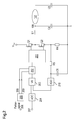
- Fig.1 shows a block diagram with a control gear for driving a lamp 101st
- An error signal 107 is detected by the input of a logic circuit 104, the output of the logic circuit controls a current source 105 which can provide a current I F (fault current) at a node 108.
- the node 108 is connected to the input of a voltage controlled oscillator (VCO) 103, the outputs of which are a half-bridge circuit comprising mosfets Q1 and Q2, in particular the gate terminals of Mosfets Q1, Q2 drive.
- VCO voltage controlled oscillator
- the drain terminal of the MOSFET Q2 is connected to the source terminal of the MOSFET Q1 and to a node 109 via an inductance L1.
- the drain terminal of the MOSFET Q1 is connected to a supply voltage V bus of the half-bridge circuit, and the source terminal of the MOSFET Q2 is connected to ground via a resistor R4.
- the source terminal of the MOSFET Q2 is also connected via a resistor R1 to the noninverting input of an operational amplifier 102, which is further connected to ground via a capacitor C1.
- an operational amplifier 102 At the inverting input of the operational amplifier 102 is a setpoint 106 at.
- the inverting input is connected to the node 108 via a capacitor C3.
- the output of the operational amplifier 102 is connected to the node 108 via a diode D1, the cathode of the diode D1 pointing in the direction of the node 108.
- the node 108 is connected to ground via a resistor R2. Also, the node 108 is connected to ground via a capacitor C2.
- the lamp 101 is connected on the one hand to the node 109 and on the other hand via a capacitor C5 to ground. Between the node 109 and ground, a capacitor C4 is arranged.
- the operational amplifier 102 performs a target-actual comparison between the predetermined value 106 (set point) and a voltage across the resistor R4 (actual value) filtered by the RC element comprising the resistor R1 and the capacitor Cl.
- the operational amplifier 102 controls the voltage-controlled oscillator 103 via the diode D1 and thus determines the respectively suitable operating frequency of the half-bridge circuit comprising the MOSFETs Q1 and Q2.
- the half-bridge circuit supplies the lamp 101 with the required power via the inductance L1 and the capacitors C4 and C5.
- the logic circuit 104 receives the error signal 107 and drives the current source 105, which charges the capacitor C2 with the fault current I F. This increases the voltage at the node 108 and thus the operating frequency of the half-bridge circuit.
- the operational amplifier 102 tries to counteract, but due to the decoupling by the diode D1 can not lower the voltage at the voltage-controlled oscillator 103 and thus the operating frequency of the half-bridge circuit.
- the operational amplifier 102 again controls the operating frequency of the half-bridge circuit.
- Fig.2 shows a schematic block diagram for a digital approach.
- a frequency counter 201 is used to drive the half-bridge circuit including the mosfets Q1, Q2.
- the half-bridge circuit and the lamp 101 connected thereto with wiring via the inductance L1, the capacitors C4 and C5, and the Resistor R4 correspond to the in Fig.1 illustrated circuit.
- An error signal 206 is connected to the input of a logic circuit 205.
- the logic circuit 205 has an output 208 indicating the operating mode (normal mode or error mode). Furthermore, the logic circuit 205 has an output 209, which indicates a frequency for driving the half-bridge circuit. The outputs 208 and 209 are connected to a switching unit 202.
- a setpoint value 207 is forwarded via an analog-digital converter 204 to a digital processing unit 203 (VE, controller) whose output is connected to the input of the frequency counter 201 via the switching unit 202.
- VE digital processing unit
- the source terminal of the MOSFET Q2 is connected via a resistor R5 to the input of an analog-to-digital converter 210.
- the input of the analog-to-digital converter 210 is connected to ground via a capacitor C6 and the output of the analog-to-digital converter 210 is connected to an input of the processing unit 203.
- the digital processing unit 203 performs a target-actual comparison by comparing the target value 207 with an actual value.
- the actual value is a voltage across the resistor R4, which is filtered by means of the RC element from the resistor R5 and the capacitor C6.
- Analogue setpoint 207 is converted by analog-to-digital converter 204, and the voltage value at resistor R4 is converted to a digital value by analog-to-digital converter 210.
- the processing unit 203 controls the frequency counter 201 and thus determines the respectively appropriate operating frequency of the half-bridge Q1, Q2, which in turn via the inductance L1 in combination supplied with the capacitors C4 and C5, the lamp 101 with the desired power.
- the logic circuit 205 receives the error signal 206 and controls the frequency counter 201 itself. This is achieved by the logic circuit 205 (via its output 208) the switching unit 202 controls so that the provided at the output 209 frequency sets the frequency counter 201 directly.
- the logic circuit 205 transfers control of the frequency back to the digital processing unit 203.
- the digital processing unit 203 is relatively slow and prescribes computation cycles that only relatively rarely (for example every 100 ⁇ s) makes it possible to update the frequency of the frequency counter 201.
- This effect is further compounded in that the analog-to-digital converters 204 and 210 require a processing time (e.g., about 10 ⁇ s) to convert the analog signals.
- a resulting dead time of about 110 ⁇ s can significantly affect the stability of the control.
- the object of the invention is to avoid the above-mentioned disadvantages and in particular to provide an efficient way of controlling a lamp.
- a circuit for driving a lamp in particular a fluorescent lamp
- the lamp is connected via a bridge circuit, e.g. a full or half bridge circuit operated.
- the circuit comprises analog control (e.g., an analog control circuit) for driving the bridge circuit in a first mode of operation and a logic circuit (e.g., digital control circuit) for driving the bridge circuit in a second mode of operation.
- the circuit has only small delays due to required signal conversion and thus the dead time of the analog control in the first operating mode is low compared to a purely digital control. This achieves a high degree of control stability. Furthermore, it is an advantage that the processing of the signals in the two operating modes can be carried out separately from one another and that an effective decoupling of the operating modes is achieved in this way.
- the first operating mode is a normal mode in which the lamp is lit and, in particular, neither too high an output voltage of the circuit nor too high a current in the bridge circuit occurs.
- the lamp In normal mode, the lamp is operated (e.g., dimmed) and lights up accordingly.
- the second operating mode is an error mode comprising in particular a preheat mode and / or an ignition mode in which the lamp is not lit in particular.
- the operating mode includes, for example, all modes in which the lamp is not (yet) lit or all modes that do not correspond to the normal mode, such as an excessively high output voltage or an overcurrent in the Bridge circuit.
- the ignition mode is shortly before or during the ignition of the lamp such a second mode of operation.
- the preheat mode is a second mode of operation before the lamp is lit.
- the failure mode includes a state in which the lamp lights, in particular, the circuit has an output voltage which is greater than a predetermined voltage threshold and / or wherein in the bridge circuit, a current flows greater than is a predetermined current threshold.
- the failure mode may also include the state of an overvoltage at the output of the circuit or an overcurrent in the bridge circuit.
- the bridge circuit has a half-bridge circuit with two electronic switches, in particular two transistors or two MOSFETs, whose center tap is connected to the lamp via an inductance.
- the bridge circuit may also comprise a full bridge circuit.
- the bridge circuit can be controlled via a frequency counter, wherein the analog control is connected in the first operating mode with the frequency counter via an analog-to-digital converter.
- the analog control provides an analog signal which is converted to a digital signal via the analog-to-digital converter and used to drive the frequency counter.
- the frequency counter is a unit for driving the bridge circuit, in particular for driving electronic switches (for example MOSFETs or transistors) of a half bridge or a full bridge circuit.
- the frequency counter converts a digital input signal, which corresponds to a frequency, into the control of the bridge circuit. The higher the frequency, the faster the control of the electronic switches provided by the frequency counter changes.
- the logic circuit causes the switching between the first operating mode and the second operating mode via a control signal, in particular via a further output, which is connected to the switching unit.
- the logic circuit controls, by means of the switching unit, the change between the first operating mode in which the analog control drives the bridge circuit and the second operating mode in which the logic circuit provides a frequency for driving the bridge circuit.
- a changeover between the first operating mode and the second operating mode can take place if the error signal is detected.
- the error signal may indicate that it is not normal operation of the lamp, i. that the lamp is e.g. is not lit or that it is lit, but the voltage dropping across it is too high or the current in the bridge circuit is too high. Based on (the detection) of the error signal, the second operating mode can be started.
- the error signal may indicate, in particular, that ignition or preheating of the lamp is required.
- the analog control comprises an operational amplifier whose inverting input is connected to a desired value whose inverting input is connected via a capacitor to the output and at whose non-inverting input an actual value of a lamp power or a lamp current can be determined.
- the setpoint may be a dimming value, i. a value corresponding to a brightness preset for setting the lamp. This value can e.g. be set by a user via a voltage divider or a voltage source with a variable resistor.
- an alternative embodiment is that during the second operating mode, as long as the lamp is not lit, the analog control is set so that an output signal provided by it for driving the bridge circuit corresponds to a frequency between the operating frequency during preheating and the operating frequency when ignited.
- the analog control in the second operating mode as long as the lamp is not lit and while it does not control the bridge circuit are preset such that when switching to the first operating mode (ie when taking over the control by the analog control) a Zündblitz is prevented.
- the analog control is set, for example, such that its analog or digitized output signal corresponds to an operating frequency for the bridge circuit, which lies between the preheat frequency and the ignition frequency.
- a next embodiment is that the output signal of the analog control corresponds to an average value of the voltage for the current operating frequency f and a voltage for a preheating frequency f max .
- the output signal of the analog control can be adjusted so that it controls a drive of the half-bridge circuit with a frequency of f / 2 + f Max / 2 where f is the current operating frequency and f max is the preheat frequency.
- Another embodiment is that during the second mode of operation, when the lamp is lit but its voltage is too high or the current in the bridge circuit is too high, the logic circuit gradually increases the operating frequency.
- the analog control determines a deviation and gives in the attempt to eliminate them, a minimum operating frequency.
- the logic circuit can gradually reduce the frequency again. As soon as the control deviation is minimal (equal to zero or less than a predefined threshold value), the frequency specification of the analog control jumps to the current operating frequency. Then, the second operating mode is switched back to the first operating mode.
- a minimum operating frequency can be limited with increasing temperature.
- a development consists in that a temperature-dependent voltage limitation is provided, by means of which a lower threshold value of a signal provided by the analog controller can be limited depending on the temperature.
- a temperature dependent voltage may be added to the output voltage of the analog controller (e.g., the operational amplifier).
- a lamp, luminaire or lighting module comprising at least one of the circuits described here.
- Figure 3 shows a schematic block diagram with an electronic control gear for a lamp 101st
- An error signal 306 is connected to the input of a logic circuit 305.
- the logic circuit 305 has an output 308 indicating the operating mode (normal mode or error mode). Furthermore, the logic circuit 305 has an output 309, which indicates a frequency for driving a half-bridge circuit.
- the outputs 308 and 309 are connected to a switching unit 302.
- a set point 307 (e.g., a user-adjustable dimming value, i.e., a value for adjusting the brightness of the lamp) is provided to an inverting input of an operational amplifier 304, the inverting input being connected to the output of the operational amplifier 304 via a capacitor C8.
- the output of the operational amplifier 304 is further connected to the switching unit 302 via an analog-to-digital converter 303.
- the switching unit 302 is connected on the output side to the input of the frequency counter 301.
- the outputs of the frequency counter 301 are connected to the half-bridge circuit comprising MOSFETs Q1 and Q2, in particular to the gate terminals of the MOSFETs Q1, Q2.
- the drain terminal of the MOSFET Q2 is connected to the source terminal of the MOSFET Q1 and via an inductance L1 with connected to a node 109.
- the drain terminal of the MOSFET Q1 is connected to a supply voltage V bus of the half-bridge circuit, and the source terminal of the MOSFET Q2 is connected to ground via a resistor R4.
- the lamp 101 is connected on the one hand to the node 109 and on the other hand via a capacitor C5 to ground. Between the node 109 and ground, a capacitor C4 is arranged.
- the source terminal of the MOSFET Q2 is connected via a resistor R6 to the noninverting input of the operational amplifier 304, which is connected to ground via a capacitor C7.
- the lamp 101 may be, for example, a fluorescent lamp.
- the (analog) operational amplifier 304 acts as an analog controller and performs a nominal-actual comparison of analog voltages: the (predetermined) setpoint value 307 is compared with the voltage dropping across the resistor R4, this voltage being measured using the RC- Element from the resistor R6 and the capacitor C7 is filtered.
- the output signal provided by the operational amplifier 304 is converted into a digital signal by means of the analog-to-digital converter 303 and used in the normal mode for controlling the frequency counter 301 (in the normal mode, the operational amplifier 304 is informed via the analog-to-digital converter 303 by the switching unit 302 the frequency counter 301 connected).
- the operational amplifier 304 determines the operating frequency of the half-bridge circuit comprising the MOSFETs Q1, Q2, which supplies the lamp 101 with the desired power via the inductance L1 in conjunction with the capacitors C4 and C5.
- the controller as a whole has a high level of control stability.
- Another advantage is that the analog controller and the logic circuit are effectively decoupled from each other.
- the operating frequency of the frequency counter 301 is digitally adjustable.
- the logic circuit 305 drives the frequency counter 301 for a period of about 0.5 seconds to provide the relatively high preheat frequency for the lamp 101. At this time, the voltage dropped across the lamp 101 is small and its electrodes are preheated. After this period, the logic circuit 305 lowers the frequency up to an ignition frequency. At the ignition frequency, the voltage required to ignite the lamp 101 is generated by a resonance increase of the LC element from the inductance L1 and the capacitor C4. As soon as the voltage exceeds the required value, the frequency is raised again. If no more overvoltage is detected, the frequency is lowered again. In this way, the voltage can be adjusted to a required value until the lamp has ignited. Now, the operational amplifier 304 takes over the frequency control, the normal operation is achieved.
- the logic circuit 305 receives the error signal 306 and controls the frequency counter 301 itself. This is accomplished by the logic circuit 305 driving (via its output 308) the switching unit 302 to control that at the output 309 directly sets the frequency counter 301.
- the logic circuit 305 may incrementally increase the frequency. If the error no longer exists, the logic circuit 305 may gradually reduce the frequency until the control deviation has disappeared and the operational amplifier 304 may resume frequency control.
- the raising and lowering of the operating frequency can take place at different speeds.
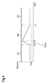
- Figure 4 contains a diagram showing the operating frequency with which the half-bridge circuit is driven, for different modes of control.
- the operational amplifier 304 sets the operating frequency. This operating frequency is for example constant, it is the normal mode.
- the logic circuit increments the operating frequency until the error disappears at a time t2 (in FIG Figure 4 an infinite increase in the operating frequency is shown as an example).
- the logic circuit gradually reduces the operating frequency (if the fault does not recur) until a time t3 (in FIG Figure 4 symbolically represented as a continuous decrease of the operating frequency).
- the stationary value of the operating frequency is reached again and the operational amplifier 304 takes over the frequency control. In that regard, the normal mode in a period 403 is reached again.
- the period 402 between times t1 and t3 may be referred to as an error mode.
- the logic circuit 305 outputs a higher frequency than is suitable for satisfying the setpoint setting, so that the operational amplifier 304 detects a control deviation and tries to eliminate it Output sets to OV, which corresponds to the minimum operating frequency f min of the half-bridge circuit.
- the operational amplifier 304 keeps its output in the ignition mode at OV.
- the lamp 101 has ignited and the control of the operating frequency is transferred by means of the switching device 302 to the operational amplifier 304, the latter operates the lamp 101 first with the lowest possible frequency, ie with the highest power. A reduction of the power to the desired value takes place only delayed due to the arranged in the negative feedback capacitor C8. This can cause a disturbing ignition flash.
- This ignition flash can be prevented as follows: The operating frequency in the lowest dimming position is approximately halfway between the preheat frequency and the firing frequency. This also applies at higher temperatures at which the lamp 101 already ignites at a lower voltage and correspondingly higher frequency.
- the output of the operational amplifier 304 is maintained at a voltage corresponding to the average of the voltage for the current operating frequency f and the voltage for the preheating frequency f max .
- the lamp 101 is first operated in the lowest dimming position and thus effectively prevents the Zündblitz.
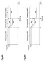
- Fig.6A and Fig.6B each show a diagram in which the operating frequency of the half-bridge circuit is shown over time.
- the lamp 101 is preheated (preheat mode 601), between the times t1 and t2 the lamp 101 is ignited (firing mode 602) and from the time t2 the lamp 101 is operated in the normal mode 603, in FIG 6A in the lowest dimming position and in 6B with full power.
- the operating frequency f max during preheat mode 601 is provided by logic circuit 305.
- the operating frequency 605 is provided by the logic circuit 305, the output of the operational amplifier 304 is set to a voltage corresponding to the operating frequency according to a curve 604. From the time t2 in the normal mode 603, the operational amplifier takes over the provision of the operating frequency (see curve 606) or the driving of the lamp 101.
- the output of the operational amplifier 304 By presetting the output of the operational amplifier 304 to a voltage which is the mean value of the preheat frequency f max and more current Operating frequency corresponds, a disturbing ignition flash can be prevented.
- Figure 5 shows based on the circuit according to Figure 3 a schematic block diagram with an electronic operating device for the lamp 101 for preventing the Zündblitzes or for presetting the operational amplifier 304.
- the differences between the circuit according to Figure 5 and the in Figure 3 illustrated circuit explained. With regard to the unchanged components, reference is made to the above statements.
- the error signal 306 is connected to the input of a logic circuit 501.
- the logic circuit 501 has, in accordance with the in Figure 3 shown logic circuit 305 has an output 308 indicating the operating mode (normal mode or error mode). Furthermore, the Logic circuit 501 via an output 309 indicating a frequency for driving the half-bridge circuit. The outputs 308 and 309 are connected to the switching unit 302.
- the emitter of the transistor Q3 is connected to the output of the operational amplifier 304 and the collector of the transistor Q3 is connected via a switch S1 to the inverting input of the operational amplifier 304.
- a resistor R7 is disposed between the collector of the transistor Q3 and ground.
- the output of operational amplifier 304 may be set to a desired voltage level by transistor Q3, which is connected in its negative feedback and controlled by logic circuit 501.
- the logic circuit 501 provides at its output 503 the digital value of a voltage for adjusting the operating frequency to the frequency f Q3 .
- the digital value is converted by means of the analog-to-digital converter 502 into a corresponding analog voltage value, which controls the transistor Q3 minus a voltage of 0.5 V to take account of the base-emitter threshold of the transistor Q3.
- the resistor R7 loads the setpoint input, which is thereby smaller than the power converted during preheating or ignition.
- the switch S1 may be an electronic switch, e.g. a transistor or mosfet, e.g. can be controlled by the drive logic 501.
- the electronic control gear in a hot environment in particular a hot light, used, it is advantageous to reduce the lamp power to thermally relieve the components of the operating device and to save energy, since at high ambient temperature, the efficiency of a fluorescent lamp decreases sharply ,
- the burning voltage of a fluorescent lamp decreases with increasing temperature.
- the electronic operating device should accordingly reduce the operating frequency. Once the lowest possible operating frequency is reached, a predetermined power reduction occurs.
- the output voltage of the operational amplifier 304 can move within a certain range, for example in one Range from OV to 3.3V.
- the downstream analog-to-digital converter 303 processes input voltages in a range of 0.5V to 3.3V. At an input voltage of 0.5V or less, the analog-to-digital converter 303 sets the frequency counter 301 to the minimum operating frequency.
- a temperature-dependent voltage limitation can be arranged between the operational amplifier 304 and the analog-to-digital converter 303, whose smallest output voltage is below a predetermined temperature, e.g. 80 ° C, less than or equal to 0.5V, above this temperature but above 0.5V.
- a predetermined temperature e.g. 80 ° C, less than or equal to 0.5V, above this temperature but above 0.5V.
- Figure 7 shows a schematic circuit diagram based on the circuits according to Figure 3 or Figure 5 comprising a temperature-dependent voltage limiting 701, which is arranged between the operational amplifier 304 and the analog-to-digital converter 303.
- Figure 8 shows an output voltage of the analog controller as a function of the temperature T.
- the output voltage can only be up to 80 ° C below 0.5V.
- the temperature-dependent voltage limitation specifies a lower threshold value greater than 0.5 V for the output voltage of the analog controller and thus limits the maximum possible lamp power.
- a temperature-dependent voltage can also be added to the output voltage of the operational amplifier 304.
- This temperature-dependent voltage can be compensated (compensated) by the operational amplifier as long as its output voltage is greater than 0V.
- the added temperature-dependent voltage acts like the limitation described above.
Landscapes
- Circuit Arrangements For Discharge Lamps (AREA)
Applications Claiming Priority (1)
| Application Number | Priority Date | Filing Date | Title |
|---|---|---|---|
| DE102010042020A DE102010042020A1 (de) | 2010-10-06 | 2010-10-06 | Schaltung und Verfahren zur Ansteuerung einer Lampe |
Publications (1)
| Publication Number | Publication Date |
|---|---|
| EP2440022A2 true EP2440022A2 (fr) | 2012-04-11 |
Family
ID=45554918
Family Applications (1)
| Application Number | Title | Priority Date | Filing Date |
|---|---|---|---|
| EP11182733A Withdrawn EP2440022A2 (fr) | 2010-10-06 | 2011-09-26 | Commutation et procédé de commande d'une lampe |
Country Status (4)
| Country | Link |
|---|---|
| US (1) | US20120086355A1 (fr) |
| EP (1) | EP2440022A2 (fr) |
| CN (1) | CN102573250A (fr) |
| DE (1) | DE102010042020A1 (fr) |
Families Citing this family (2)
| Publication number | Priority date | Publication date | Assignee | Title |
|---|---|---|---|---|
| US9152193B2 (en) | 2012-06-06 | 2015-10-06 | Apple Inc. | Power supply acoustic noise mitigation |
| TWI642271B (zh) * | 2018-05-31 | 2018-11-21 | 大陸商北京集創北方科技股份有限公司 | 具過電流保護機制的功率運算放大器及利用其之類比電路系統 |
Family Cites Families (8)
| Publication number | Priority date | Publication date | Assignee | Title |
|---|---|---|---|---|
| US5008599A (en) * | 1990-02-14 | 1991-04-16 | Usi Lighting, Inc. | Power factor correction circuit |
| US5680017A (en) * | 1996-05-03 | 1997-10-21 | Philips Electronics North America Corporation | Driving scheme for minimizing ignition flash |
| US6956336B2 (en) * | 2002-07-22 | 2005-10-18 | International Rectifier Corporation | Single chip ballast control with power factor correction |
| US7154232B2 (en) * | 2003-06-24 | 2006-12-26 | International Rectifier Corporation | Ballast control IC with multi-function feedback sense |
| TWI270839B (en) * | 2004-02-11 | 2007-01-11 | O2Micro Int Ltd | Liquid crystal display system with lamp feedback and method for controlling power to cold cathode fluorescent lamp |
| FI20065645A7 (fi) * | 2004-04-08 | 2006-11-06 | Int Rectifier Corp | PFC ja virranrajoittimen ohjausmikropiiri |
| DE102005035466A1 (de) * | 2005-07-28 | 2007-02-01 | Tridonicatco Gmbh & Co. Kg | Adaptive Regelung der Leistung von Gasentladungslampen |
| TW200810603A (en) * | 2006-08-04 | 2008-02-16 | Greatchip Technology Co Ltd | Light-modulating circuit of discharge lamp and its control method |
-
2010
- 2010-10-06 DE DE102010042020A patent/DE102010042020A1/de not_active Ceased
-
2011
- 2011-09-26 EP EP11182733A patent/EP2440022A2/fr not_active Withdrawn
- 2011-10-05 US US13/253,165 patent/US20120086355A1/en not_active Abandoned
- 2011-10-08 CN CN2011103154633A patent/CN102573250A/zh active Pending
Non-Patent Citations (1)
| Title |
|---|
| None |
Also Published As
| Publication number | Publication date |
|---|---|
| DE102010042020A1 (de) | 2012-04-12 |
| CN102573250A (zh) | 2012-07-11 |
| US20120086355A1 (en) | 2012-04-12 |
Similar Documents
| Publication | Publication Date | Title |
|---|---|---|
| DE69919138T2 (de) | Electronischer dimmer | |
| DE10026070B4 (de) | Vorschaltgerät für eine Entladungslampe | |
| DE102007002731B4 (de) | Lichtstromkreis | |
| EP1333707B1 (fr) | Ballast électronique pour une lampe à décharge | |
| EP0801881B1 (fr) | Procede permettant de faire fonctionner au moins une lampe a fluorescence au moyen d'un ballast electronique et ballast electronique utilise a cet effet | |
| DE4119204A1 (de) | Ansteuerschaltung fuer elektroluminiszenz-leuchte | |
| DE19708783C1 (de) | Verfahren und Vorrichtung zum Regeln des Betriebsverhaltens von Gasentladungslampen | |
| EP1465465B1 (fr) | Ballast électronique avec un circuit en pont complet | |
| EP1467474A2 (fr) | Circuit d'interface pour opérer des charges capacitives | |
| WO1995002914A1 (fr) | Systeme d'alimentation en tension continue fonctionnant en tampon | |
| DE102010042020A1 (de) | Schaltung und Verfahren zur Ansteuerung einer Lampe | |
| DE60127966T2 (de) | Schaltungsanordnung | |
| DE10209631A1 (de) | Elektronische Schaltung und Verfahren zur Energieversorgung einer Hochdruckgasentladungslampe | |
| EP2256927B1 (fr) | Etalonnage et commande d'amorçage des interrupteurs dans un équipement d'exploitation pour des éléments lumineux | |
| DE69113461T2 (de) | Solarbetriebene lampe. | |
| EP2595457A2 (fr) | Procédé et installation pour le fonctionnement d'un ventilateur par le biais du signal à largeur d'impulsion modulée d'un appareil placé en amont | |
| EP2452543B1 (fr) | Procédé pour faire fonctionner des lampes à décharge de gaz à des températures extérieures basses et appareil de fonctionnement conçu à cet effet | |
| EP3393207A1 (fr) | Régulateur de commutation destiné au fonctionnement de moyens lumineux à suppression de luminescence résiduelle | |
| DE10235217A1 (de) | Schaltungsvorrichtung und Verfahren zum Betreiben einer Lampe | |
| EP1618766B1 (fr) | Circuit d'allumage a regulation de la tension d'allumage | |
| EP1280388B1 (fr) | Ballast électronique avec un mode de préchauffage | |
| EP2409552B1 (fr) | Circuit et systeme pour regulation d'un source lumineuse | |
| EP0485865A1 (fr) | Circuit pour alimenter une lampe à décharge | |
| DE2622392A1 (de) | Automatische beleuchtungsregelung | |
| EP1708344B1 (fr) | Procédé et dispositif pour réguler une alimentation de puissance à découpage |
Legal Events
| Date | Code | Title | Description |
|---|---|---|---|
| AK | Designated contracting states |
Kind code of ref document: A2 Designated state(s): AL AT BE BG CH CY CZ DE DK EE ES FI FR GB GR HR HU IE IS IT LI LT LU LV MC MK MT NL NO PL PT RO RS SE SI SK SM TR |
|
| AX | Request for extension of the european patent |
Extension state: BA ME |
|
| PUAI | Public reference made under article 153(3) epc to a published international application that has entered the european phase |
Free format text: ORIGINAL CODE: 0009012 |
|
| RAP1 | Party data changed (applicant data changed or rights of an application transferred) |
Owner name: OSRAM GMBH |
|
| RAP1 | Party data changed (applicant data changed or rights of an application transferred) |
Owner name: OSRAM GMBH |
|
| STAA | Information on the status of an ep patent application or granted ep patent |
Free format text: STATUS: THE APPLICATION IS DEEMED TO BE WITHDRAWN |
|
| 18D | Application deemed to be withdrawn |
Effective date: 20150401 |