EP2443594B1 - Widerstandsbewertung des kopplungsfaktors eines elektromagnetischen transponders - Google Patents
Widerstandsbewertung des kopplungsfaktors eines elektromagnetischen transponders Download PDFInfo
- Publication number
- EP2443594B1 EP2443594B1 EP10734222.2A EP10734222A EP2443594B1 EP 2443594 B1 EP2443594 B1 EP 2443594B1 EP 10734222 A EP10734222 A EP 10734222A EP 2443594 B1 EP2443594 B1 EP 2443594B1
- Authority
- EP
- European Patent Office
- Prior art keywords
- transponder
- terminal
- value
- coupling
- voltage
- Prior art date
- Legal status (The legal status is an assumption and is not a legal conclusion. Google has not performed a legal analysis and makes no representation as to the accuracy of the status listed.)
- Active
Links
Images

Classifications
-
- G—PHYSICS
- G06—COMPUTING OR CALCULATING; COUNTING
- G06K—GRAPHICAL DATA READING; PRESENTATION OF DATA; RECORD CARRIERS; HANDLING RECORD CARRIERS
- G06K19/00—Record carriers for use with machines and with at least a part designed to carry digital markings
- G06K19/06—Record carriers for use with machines and with at least a part designed to carry digital markings characterised by the kind of the digital marking, e.g. shape, nature, code
- G06K19/067—Record carriers with conductive marks, printed circuits or semiconductor circuit elements, e.g. credit or identity cards also with resonating or responding marks without active components
- G06K19/07—Record carriers with conductive marks, printed circuits or semiconductor circuit elements, e.g. credit or identity cards also with resonating or responding marks without active components with integrated circuit chips
- G06K19/0723—Record carriers with conductive marks, printed circuits or semiconductor circuit elements, e.g. credit or identity cards also with resonating or responding marks without active components with integrated circuit chips the record carrier comprising an arrangement for non-contact communication, e.g. wireless communication circuits on transponder cards, non-contact smart cards or RFIDs
-
- G—PHYSICS
- G06—COMPUTING OR CALCULATING; COUNTING
- G06K—GRAPHICAL DATA READING; PRESENTATION OF DATA; RECORD CARRIERS; HANDLING RECORD CARRIERS
- G06K19/00—Record carriers for use with machines and with at least a part designed to carry digital markings
- G06K19/06—Record carriers for use with machines and with at least a part designed to carry digital markings characterised by the kind of the digital marking, e.g. shape, nature, code
- G06K19/067—Record carriers with conductive marks, printed circuits or semiconductor circuit elements, e.g. credit or identity cards also with resonating or responding marks without active components
- G06K19/07—Record carriers with conductive marks, printed circuits or semiconductor circuit elements, e.g. credit or identity cards also with resonating or responding marks without active components with integrated circuit chips
- G06K19/0701—Record carriers with conductive marks, printed circuits or semiconductor circuit elements, e.g. credit or identity cards also with resonating or responding marks without active components with integrated circuit chips at least one of the integrated circuit chips comprising an arrangement for power management
-
- G—PHYSICS
- G06—COMPUTING OR CALCULATING; COUNTING
- G06K—GRAPHICAL DATA READING; PRESENTATION OF DATA; RECORD CARRIERS; HANDLING RECORD CARRIERS
- G06K19/00—Record carriers for use with machines and with at least a part designed to carry digital markings
- G06K19/06—Record carriers for use with machines and with at least a part designed to carry digital markings characterised by the kind of the digital marking, e.g. shape, nature, code
- G06K19/067—Record carriers with conductive marks, printed circuits or semiconductor circuit elements, e.g. credit or identity cards also with resonating or responding marks without active components
- G06K19/07—Record carriers with conductive marks, printed circuits or semiconductor circuit elements, e.g. credit or identity cards also with resonating or responding marks without active components with integrated circuit chips
- G06K19/0701—Record carriers with conductive marks, printed circuits or semiconductor circuit elements, e.g. credit or identity cards also with resonating or responding marks without active components with integrated circuit chips at least one of the integrated circuit chips comprising an arrangement for power management
- G06K19/0702—Record carriers with conductive marks, printed circuits or semiconductor circuit elements, e.g. credit or identity cards also with resonating or responding marks without active components with integrated circuit chips at least one of the integrated circuit chips comprising an arrangement for power management the arrangement including a battery
-
- G—PHYSICS
- G06—COMPUTING OR CALCULATING; COUNTING
- G06K—GRAPHICAL DATA READING; PRESENTATION OF DATA; RECORD CARRIERS; HANDLING RECORD CARRIERS
- G06K19/00—Record carriers for use with machines and with at least a part designed to carry digital markings
- G06K19/06—Record carriers for use with machines and with at least a part designed to carry digital markings characterised by the kind of the digital marking, e.g. shape, nature, code
- G06K19/067—Record carriers with conductive marks, printed circuits or semiconductor circuit elements, e.g. credit or identity cards also with resonating or responding marks without active components
- G06K19/07—Record carriers with conductive marks, printed circuits or semiconductor circuit elements, e.g. credit or identity cards also with resonating or responding marks without active components with integrated circuit chips
- G06K19/0701—Record carriers with conductive marks, printed circuits or semiconductor circuit elements, e.g. credit or identity cards also with resonating or responding marks without active components with integrated circuit chips at least one of the integrated circuit chips comprising an arrangement for power management
- G06K19/0715—Record carriers with conductive marks, printed circuits or semiconductor circuit elements, e.g. credit or identity cards also with resonating or responding marks without active components with integrated circuit chips at least one of the integrated circuit chips comprising an arrangement for power management the arrangement including means to regulate power transfer to the integrated circuit
-
- G—PHYSICS
- G06—COMPUTING OR CALCULATING; COUNTING
- G06K—GRAPHICAL DATA READING; PRESENTATION OF DATA; RECORD CARRIERS; HANDLING RECORD CARRIERS
- G06K19/00—Record carriers for use with machines and with at least a part designed to carry digital markings
- G06K19/06—Record carriers for use with machines and with at least a part designed to carry digital markings characterised by the kind of the digital marking, e.g. shape, nature, code
- G06K19/067—Record carriers with conductive marks, printed circuits or semiconductor circuit elements, e.g. credit or identity cards also with resonating or responding marks without active components
- G06K19/07—Record carriers with conductive marks, printed circuits or semiconductor circuit elements, e.g. credit or identity cards also with resonating or responding marks without active components with integrated circuit chips
- G06K19/0723—Record carriers with conductive marks, printed circuits or semiconductor circuit elements, e.g. credit or identity cards also with resonating or responding marks without active components with integrated circuit chips the record carrier comprising an arrangement for non-contact communication, e.g. wireless communication circuits on transponder cards, non-contact smart cards or RFIDs
- G06K19/0726—Record carriers with conductive marks, printed circuits or semiconductor circuit elements, e.g. credit or identity cards also with resonating or responding marks without active components with integrated circuit chips the record carrier comprising an arrangement for non-contact communication, e.g. wireless communication circuits on transponder cards, non-contact smart cards or RFIDs the arrangement including a circuit for tuning the resonance frequency of an antenna on the record carrier
Definitions
- the present invention generally relates to electronic systems and more particularly to systems using electromagnetic transponders, that is to say transceivers that can be interrogated without contact and wirelessly by a reading terminal and / or writing.
- Communication systems based on a modulation of an electromagnetic field generated by a terminal are multiple. This ranges from a simple electronic tag used as an antitheft device to more complex systems where a transponder, having to communicate with the terminal in whose field it is, is equipped with calculation functions (electronic wallet for example) or with processing. of information.
- the electromagnetic transponder systems are based on the use of oscillating circuits comprising an antenna winding, transponder side and terminal side. These circuits are intended to be coupled by close magnetic field when the transponder enters the field of the terminal.
- the oscillating circuits of the terminal and the transponder are generally tuned to the same frequency corresponding to the excitation frequency of the oscillating circuit of the terminal.
- the transponders are devoid of autonomous power supply and extract the power required for the circuits they comprise of the high frequency field radiated by the antenna of the terminal.
- the quality of the communication and the possible transfer of energy depends on the coupling between the terminal and the transponder.
- This coupling which is inversely proportional (non-linear) to the distance between the terminal and the transponder, conditions the amplitude of the voltage recovered by the transponder. There is therefore a need to be able to evaluate the current coupling factor between a transponder and a terminal in the field of which it is located.
- the transponder recovers a supply voltage that strongly depends on the coupling, and therefore the consumption of the transponder circuits. For example, a decrease in the load (transponder consumption) leads to an increase in voltage and remote power. Depending on the current value of the coupling with respect to the optimum coupling, it may occur that a decrease in the load causes the coupling to approach the critical optimum coupling.
- the transponder is then in a paradoxical situation where its circuits consume less but where the voltage and remote power supply reach a maximum. For a current coupling k close to the optimum coupling, this maximum of remotely powered power is not consumed by the transponder circuits and the power must therefore be dissipated in the resonant circuit, causing the antenna to overheat. This overheating can even cause the disconnection of the contacts of the antenna, thus the destruction of the transponder.
- a conventional solution consists in detuning the transponder when the voltage at the terminals of the oscillating circuit exceeds a threshold.
- the document GB-A-2321725 discloses a method for dissipating excessive power received by a non-contact device.
- the document EP-A-1045325 discloses a distance detection method between an electromagnetic transponder and a terminal.
- An electromagnetic transponder as defined in claim 5 is also provided.
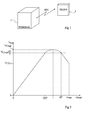
- the figure 1 is a block diagram of an electromagnetic transponder communication system.
- a terminal 1 (TERMINAL) is capable of communicating in the near field (for example according to an NFC protocol - Near Field Communication) with a remote element, namely a transponder 2 (TRANS).
- TERMINAL a terminal 1
- TRANS transponder 2
- the terminal can take various forms, for example, a ticket validation terminal, an electronic passport reader, a laptop, a mobile communication device (cellular phone, personal digital assistant - PDA, etc.), a box electronic starting of a motor vehicle, etc.
- a ticket validation terminal an electronic passport reader
- a laptop a mobile communication device (cellular phone, personal digital assistant - PDA, etc.), a box electronic starting of a motor vehicle, etc.
- the transponder can also take different forms, for example, a smart card, an electronic transport ticket, an electronic passport, a telecommunication terminal (cell phone, PDA, etc.), an electronic tag, etc.
- the figure 2 represents, very schematically and simplified, an example of terminal 1 and transponder 2.
- the terminal 1 comprises an oscillating circuit, generally series, formed of an inductance L1 in series with a capacitor C1 and a resistor R1.
- This series oscillating circuit is, in the example of the figure 2 connected between an output terminal 12 of an antenna amplifier or coupler 14 and a terminal 13 at a reference potential (generally ground).
- An element 15 for measuring the current in the oscillating circuit is interposed, for example, between the capacitive element C1 and the ground 13. This measuring element 15 is part of a phase control loop which will be described later.
- the amplifier 14 receives a high frequency transmission signal from a modulator 16 (MOD) which receives a reference frequency (OSC signal) for example from a quartz oscillator (not shown).
- MOD modulator 16
- OSC signal reference frequency
- the modulator 16 receives, if necessary, a signal Tx coming from a control circuit 11 for controlling and operating the transmissions.
- This circuit 11 is generally provided with a microprocessor for processing commands and data, communicating with different input / output circuits (keyboard, screen, exchange element with a server, etc.) and / or non-detailed processing .
- the elements of the terminal 1 derive most often the energy necessary for their operation from a supply circuit (not shown) connected, for example, to the electrical distribution network (mains) or to a battery (for example, that of 'a motor vehicle or a phone or laptop).
- the modulator 16 provides a high frequency carrier (for example, at 13.56 MHz) to the L1-C1 series oscillating circuit which generates a magnetic field.
- the capacitive element C1 is, for example, a variable capacitance element and controllable by a CTRL signal. This element participates in the phase regulation of the current I1 in the antenna L1 with respect to a reference signal.
- This regulation is a regulation of the high frequency signal, that is to say the signal of the carrier corresponding to the signal supplied to the amplifier 14 in the absence of Tx data to be transmitted.
- the regulation is performed by varying the capacitance C1 of the oscillating circuit of the terminal so as to maintain the current in the antenna in constant phase relation with a reference signal.
- This reference signal corresponds, for example, to the signal OSC supplied to the modulator 14.
- the signal CTRL comes from a circuit 17 (COMP) whose role is to detect the phase difference with respect to the reference signal and to modify accordingly the capacity of the element C1.
- the comparator receives a MES information on the current I1 in the oscillating circuit detected by the measuring element 15 (for example, an intensity transformer or a resistor).
- a transponder 2 capable of cooperating with the terminal 1, comprises an oscillating circuit, for example a parallel circuit, formed of an inductor L2 in parallel with a capacitor C2 between two terminals 21 and 22.
- the parallel oscillating circuit (called the resonant circuit on reception ) is intended to capture the magnetic field generated by the oscillating circuit L1-C1 of the terminal 1.
- the circuits L2-C2 and L1-C1 are tuned to the same resonance frequency (for example 13.56 MHz).
- the terminals 21 and 22 are connected to two alternative input terminals of a rectifier bridge 23 (usually double alternation).
- the rectified output terminals of the bridge 23 respectively define a positive terminal 24 and a reference terminal 25.
- a capacitor Ca is connected between the terminals 24 and 25 so as to smooth the rectified voltage. If necessary, the recovered energy is used to recharge a battery not shown.
- a high frequency voltage is generated at the terminals of the resonant circuit L2-C2.
- This voltage rectified by the bridge 23 and smoothed by the capacitor Ca, supplies a supply voltage to electronic circuits of the transponder via a voltage regulator 26 (REG).
- These circuits generally comprise a processing unit 27 (for example a microcontroller ⁇ C) associated with a memory (not represented), a demodulator 28 (DEM) of the signals possibly received from the terminal 1, and a modulator 29 (MOD). to transmit information to the terminal.
- the transponder is generally synchronized by means of a clock (CLK) extracted, by a block 20, from the recovered high frequency signal, before rectification, on one of the terminals 21 or 22. Most commonly, all the electronic circuits of the transponder 2 are integrated in the same chip.
- CLK clock
- the circuit 16 modulates (generally in amplitude) the carrier (signal OSC) as a function of the signal Tx.
- these data are demodulated by the demodulator 28 from the voltage V Ca. If necessary, the demodulator takes the signal to be demodulated upstream of the rectifier bridge.
- the modulator 29 controls a modulation stage 30 (retromodulation) of the load formed by the transponder circuits on the magnetic field produced by the terminal.
- This stage generally consists of an electronic switch K30 (for example, a transistor) and a resistor R30 (or a capacitor), in series between the terminals 24 and 25.
- the switch K30 is controlled at a frequency (for example, 847.5 kHz) said subcarrier, significantly lower (usually with a ratio of at least 10) to the frequency of the excitation signal of the oscillating circuit of the terminal 1.
- the transponder oscillating circuit is subjected to additional damping with respect to the load formed by the circuits 20, 26, 27, 28, and 29 so that the transponder takes a larger amount of energy from the high frequency magnetic field.
- the amplifier 14 keeps the amplitude of the high frequency excitation signal constant. Consequently, the variation of energy of the transponder results in a variation of amplitude and phase of the current in the antenna L1. This variation is detected by an amplitude or phase demodulator of the terminal.
- the comparator 17 integrates a demodulator phase also used to demodulate the signal from the transponder. Therefore, this comparator 17 provides a signal Rx restoring a possible retromodulation of data received from a transponder to the circuit 11.
- Other demodulation circuits may be provided, for example a circuit using a measurement of the voltage across the capacitor C1 .
- the response time of the phase control loop is long enough not to hinder the possible retromodulation from a transponder, and sufficiently short in front of the speed of passage of a transponder in the field of the terminal.
- Static control over modulation frequencies can be used (for example, the 13.56 MHz remote power carrier frequency and the 847.5 kHz retrofit frequency used to transmit transponder data to the terminal).
- phase-regulated terminal An example of a phase-regulated terminal is described in the document EP-A-0 857 981 .
- the coupling coefficient between the oscillating circuit of the terminal and that of the transponder essentially depends on the distance separating the transponder from the terminal.
- k Opt The ⁇ 2 The ⁇ 1 ⁇ R ⁇ 1 R ⁇ 2 , where R2 represents the resistance equivalent to the load (load) constituted by the elements of the transponder on its own oscillating circuit.
- the resistor R2 represents the equivalent resistance of all the circuits (microprocessor, means of retromodulation, etc.) of the transponder 2, brought in parallel on the capacitor C2 and the inductance L2 (before or after the bridge rectifier ).
- resistive load the conductance provided by the transponder circuits, so their consumption.
- the level of this charge is symbolized by the resistance R2 in parallel across the oscillating circuit.
- the series resistance of inductance L1 terminal antenna
- the value of this series resistance is, for simplicity, included in the value of the resistor R1.
- the figure 3 represents an example of the shape of the voltage V C2 recovered on the transponder side as a function of the normalized coupling k / k opt with respect to the optimum coupling.
- the curve starts from the origin of ordinates (zero voltage) for a null coupling. This corresponds to a distance from the transponder and the terminal such that no signal is picked up by the transponder.
- V C2 I ⁇ 2 ⁇ ⁇ VS 2 , where 12 represents the current in the oscillating circuit of the transponder, and where ⁇ represents the pulse of the signal.
- I ⁇ 2 M ⁇ ⁇ ⁇ I ⁇ 1 Z ⁇ 2 , where I1 represents the current in the oscillating circuit of the terminal and where Z2 represents the impedance of the transponder.
- V C2tun is obtained when the latter is tuned, the formula :
- V VS ⁇ 2 k ⁇ The ⁇ 1 The ⁇ 2 ⁇ vg R ⁇ 1 R ⁇ 2 + k 2 ⁇ The ⁇ 1 The ⁇ 2 .
- V C2 (kopt) is therefore given by the formula (combining formulas 2 and 9):
- V VS ⁇ 2 ⁇ k opt vg 2 ⁇ R ⁇ 2 R ⁇ 1 .
- V VS ⁇ 2 2 ⁇ V VS ⁇ 2 ⁇ k opt k k Opt + k Opt k .
- This maximum power transferred from the terminal to the transponder is distributed between the resistor own losses in the resonant circuit and the resistor R2 corresponding to the consumption level of the transponder circuits.
- the current consumed becomes too low, it means that the value of R2 becomes very large and is therefore negligible compared with the resistor L2-C2 resonant circuit.
- the transferred power must be dissipated in this resistance of the LC circuit, which may damage the antenna.
- the figure 4 illustrates the effects of a detuning of the oscillating circuit according to the position of the coupling with respect to the optimum coupling.
- This figure shows examples of the steps of the voltage V C2 as a function of the value of the capacitor C2 for several coupling values k. It is assumed that the value of the resistance R2 does not vary.
- the maximum of the voltage V C2max is obtained at the tuning of the oscillating circuit (for simplicity, it is considered that any disagreement is caused only by a variation of the capacitance C2 and that the value of the inductance L2 remains fixed).
- the maximum voltage obtained is necessarily lower than the maximum voltage at the optimum coupling and decreases with respect to this value in case of disagreement with respect to the value C2 tun .
- the voltage V C2max can be reached even by detuning the circuit. Therefore, the disagreement of the oscillating circuit to protect from overheating is not always the solution.
- the oscillation circuit is detuned, preferably by changing the value of the capacitance C2. Indeed, it is easy to add or reduce the value of the capacitor by switching integrated capacitive elements in parallel with the capacitor C2.
- the transferred power is then partially dissipated in the resistor R2x, then reduced by detuning the oscillating circuit from k opt] R2x .
- the voltage at the terminals of the oscillating circuit is not measured directly, but the smoothed voltage across the capacitor V Ca at the output of the rectifier bridge 23.
- This voltage V Ca is proportional to the voltage V C2 .
- the measurement is performed by the microprocessor.
- the memorization of values of the measured voltages are effected, either analogically, but preferably numerically over several bits, the number of which depends on the desired analysis precision.
- the figure 5 is a flowchart illustrating an embodiment of the energy management method.
- the resistor R20 (block 47, R21-> R20) is preferably passed through.
- the ratio r is compared (block 49, h ⁇ r ⁇ H) with respect to two thresholds h and H to determine if it is within an acceptable range.
- Other values may be chosen provided, of course, that h is less than unity (preferably h is greater than 1/2) and H is greater than unity (preferably h is less than 10).
- the value of block R2x of resistance R2 is calculated (block 51, V C2opt] R2x ) according to formulas 20 and 21. to return the transponder to an optimum coupling position. Then (block 52, R20-> R2x), the value of the resistor R2 is changed to this estimated value.
- the resistive load is progressively increased by decreasing the value of R2 until the voltage V C2 reaches the value V C2opt] R2x calculated with the formula 20.
- the microcontroller interrogates a previously stored correspondence table (for example in a learning phase or during the design of the transponder) in order to know, from the value of the ratio r, the value to be given to the resistor R2.
- Test 45 is optional. Indeed, we can continue the execution of the process to move to the R2x resistor if the current coupling does not allow a disagreement. However, this test 45 makes it possible to exit the iteration more quickly if the resistance R21 proves to be sufficient.
- the figure 6 is a block diagram of an embodiment of a transponder 2, equipped to automatically determine, when in the field of a terminal (not shown), the current coupling with respect to the optimum coupling.
- the representation of the figure 6 is simplified compared to that of the figure 2 .
- the elements of demodulation, of retromodulation and of obtaining the clock frequency have not been illustrated.
- the consumption current I of the transponder circuit is measured by a resistor R sense mounted as a current detector.
- the measurement of the consumption current gives an indirect image of the equivalent resistance of the load.
- the measured value is less than or equal to the minimum value, the consumed current will be low and that, equivalently, the resistance is lower than the value R20.
- the current is lower than the minimum current, and the current coupling k is close to the optimum coupling, it is deduced that the transponder is in overheating conditions of the resonant circuit.
- the transponder 2 is based on a parallel oscillating circuit L2-C2 whose terminals 21 and 22 are connected to the input terminals of a rectifying bridge 23. Between the terminals 24 and 25 of the rectifying bridge 23 is provided a switchable resistive circuit 40. For example, two resistors R43 and R45 are connected in parallel each being in series with a switch K43, respectively K45. Switches K43 and K45 (for example, MOS transistors) are intended to be switched to implement the method of determining the coupling position.
- the processing unit 27 receives an information on the voltage V Ca on an input MES to implement the method described above.
- the resistor R2 (load of the transponder circuits) represents the value R20. Disconnection of one of the resistors (for example, resistor R43) increases resistance R2 to R21.
- Other connections and switches may be provided according to the variant of the method used. For example, a single switchable resistor can be used assuming that one of the two values of resistor R2 corresponds to the resistive load of the other transponder circuits.
- the switchable resistor corresponds to that used for resistive retromodulation.
- a first measurement is made by switching the retromodulation resistor so that it is functionally in the circuit (switch K30 in the on state in the example of FIG. figure 2 ).
- the voltage V C2] R20 is measured.
- the switch K30 is opened and the voltage V C2] R21 is measured.
- the implementation of the described method then requires no structural modification of a transponder equipped with a microcontroller. It is enough to program this microcontroller so that it switches the resistance of retromodulation.
- the thresholds used to determine the position with respect to the optimum coupling depend only on the values R20 and R21 which are known for a given transponder. Therefore, the transponder does not necessarily need advanced microprocessor-based computing means but can simply measure voltages, calculate the ratio and compare it against analog thresholds generated, for example, by resistive dividing bridges. In another example, the thresholds are precalculated and stored in a non-volatile memory of the transponder.
- the increase or decrease in the equivalent resistance R2 is caused by a variation of the consumption of the transponder circuits, typically of the processing unit 27.
- the increase or decrease in the equivalent resistance R2 is caused by a variation of the consumption of the transponder circuits, typically of the processing unit 27.
- the variation of the resistance R2 is known from the moment when the consumption of different tasks to be performed by the unit 27 is known, which is generally estimated at the transponder design or can be obtained in a learning phase with a any terminal.
- the calculations required to evaluate the current coupling are sufficiently simple so that their execution time is negligible compared to the speed of movement of a transponder in front of a terminal (thus the speed of variation of the coupling coefficient).
- the embodiments described are also applicable in the case where the transponder remains on a receiving surface of the terminal, the coupling does not vary throughout the communication.
- the figure 7 represents an embodiment of a transponder equipped with a detuning circuit of the capacitor C2.
- the transponder 2 is based on a parallel oscillating circuit L2-C2 whose terminals 21 and 22 are connected to the input terminals of a rectifying bridge 23.
- the processing unit 27 receives information about the voltage V Ca on an input MES to implement the method described above.
- the transistors Ti are individually controllable by signals from the microcontroller 27 as a function of the measurements made conditioning the desired amplitude for the mismatch.
- switchable capacitors are connected in parallel to the oscillating circuit.
- an advantage of the solution of the figure 7 is that the transistors are more easily controllable because the control signals can be referenced to the ground.
- Coupling evaluation can be performed periodically during a communication. The only precaution is not to evaluate the coupling during a retromodulation of the transponder. A first evaluation is for example performed as soon as the energy recovered by the transponder is sufficient for the microprocessor 27 to operate. Then, periodic measurements are made during the communication.
Landscapes
- Engineering & Computer Science (AREA)
- Computer Hardware Design (AREA)
- Microelectronics & Electronic Packaging (AREA)
- Physics & Mathematics (AREA)
- General Physics & Mathematics (AREA)
- Theoretical Computer Science (AREA)
- Computer Networks & Wireless Communication (AREA)
- Near-Field Transmission Systems (AREA)
- Measurement Of Resistance Or Impedance (AREA)
Claims (7)
- Ein Verfahren zum Managen der Leistung in einem elektromagnetischen Transponder (2) im Feld eines Anschlusses (1) wobei die folgenden Schritte vorgesehen sind:Auswerten (40) des Leistungsverbrauchs der Transponderschaltungen; undwenn dieser Leistungsverbrauch unterhalb einer Schwelle liegt, Auswerten des Stromkopplungsfaktors (k) zwischen dem Transponder und dem Anschluss (1) und, gemäß der Stromkopplung:Bewirken (52) einer Vergrößerung des Transponderleistungsverbrauchs; oderBewirken (50) einer Verstimmung einer Oszillatorschaltung des Transponders,wobei die Auswertung des Kopplungsfaktors einen Vergleich umfasst eines Verhältnisses (r) des Stromkopplungsfaktors des Transponders mit dem Anschluss und einer Position optimaler Kopplung (kopt]R20) mit einem ersten Wert (R20) einer Widerstandslast (R2), wobei dieses Verhältnis (r) erhalten wird aus:ersten Daten, relativ zu dem Pegel einer Gleichspannung (VCa) vorgesehen durch einen Gleichrichter (23) an der Oszillatorschaltung (L2, C2), gemessen und gespeichert (42) für den ersten Wert (R20) der Widerstandslast (R2); undzweite Daten relativ zu dem Pegel der erwähnten Gleichspannung, gemessen und gespeichert (46) für einen zweiten Wert (R21) der Widerstandslast.
- Das Verfahren nach Anspruch 1, wobei die Verstimmung (50) zu einem Wert erfolgt, der eine Fernversorgung des Transponders aufrecht erhält.
- Das Verfahren nach Anspruch 1 oder 2, wobei eine Veränderung der Widerstandslast (R2) zwischen ersten und zweiten Werten (R20, R21) erhalten wird durch modifizieren des Leistungsverbrauchs der Vearbeitungsschaltungen (27) die der Transponder aufweist.
- Das Verfahren nach Anspruch 3, wobei eine Veränderung der Widerstandslast (R2) zwischen den ersten und zweiten Werten (R20, R21) erhalten wird durch Schalten eines Widerstands-Retro-Modulationselements (30) wie es der Transponder (2) aufweist.
- Ein elektromagnetischer Transponder der folgendes aufweist:eine Oszillatorschaltung (L2, C2) stromaufwärts einer Gleichrichterschaltung (23) und in der Lage eine Gleichspannung (VCa) vorzusehen, wenn der Transponder sich im Magnetfeld eines Anschlusses (1) befindet; undmindestens eine Verarbeitungseinheit (27) programmiert zur Implementierung des Verfahrens nach irgendeinem der Ansprüche 1-4.
- Der Transponder nach Anspruch 5, der ferner mindestens ein schaltbares Widerstandselement (30, 40) aufweist, welches funktionsmäßig parallel mit der Oszillatorschaltung verbunden werden kann.
- Der Transponder nach Anspruch 5 oder 6 der mindestens ein schaltbares (Ti, T'i) kapazitives Element (C2pi, C2'pi) aufweist zum Verstimmen der Oszillatorschaltung.
Applications Claiming Priority (2)
| Application Number | Priority Date | Filing Date | Title |
|---|---|---|---|
| FR0954148A FR2947075A1 (fr) | 2009-06-19 | 2009-06-19 | Evaluation resistive du facteur de couplage d'un transpondeur electromagnetique |
| PCT/FR2010/051091 WO2010146278A1 (fr) | 2009-06-19 | 2010-06-03 | Gestion de puissance dans un transpondeur electromagnetique |
Publications (2)
| Publication Number | Publication Date |
|---|---|
| EP2443594A1 EP2443594A1 (de) | 2012-04-25 |
| EP2443594B1 true EP2443594B1 (de) | 2015-09-09 |
Family
ID=41571706
Family Applications (3)
| Application Number | Title | Priority Date | Filing Date |
|---|---|---|---|
| EP10160754.7A Active EP2267643B1 (de) | 2009-06-19 | 2010-04-22 | Widerstandsbewertung des Kopplungsfaktors eines Elektromagnetischen Transponders |
| EP10734221.4A Active EP2443593B1 (de) | 2009-06-19 | 2010-06-03 | Energiewiedergewinnung durch einen elektromagnetischen transponder |
| EP10734222.2A Active EP2443594B1 (de) | 2009-06-19 | 2010-06-03 | Widerstandsbewertung des kopplungsfaktors eines elektromagnetischen transponders |
Family Applications Before (2)
| Application Number | Title | Priority Date | Filing Date |
|---|---|---|---|
| EP10160754.7A Active EP2267643B1 (de) | 2009-06-19 | 2010-04-22 | Widerstandsbewertung des Kopplungsfaktors eines Elektromagnetischen Transponders |
| EP10734221.4A Active EP2443593B1 (de) | 2009-06-19 | 2010-06-03 | Energiewiedergewinnung durch einen elektromagnetischen transponder |
Country Status (6)
| Country | Link |
|---|---|
| US (3) | US8988196B2 (de) |
| EP (3) | EP2267643B1 (de) |
| JP (1) | JP5539056B2 (de) |
| CN (1) | CN101930034A (de) |
| FR (1) | FR2947075A1 (de) |
| WO (2) | WO2010146278A1 (de) |
Families Citing this family (19)
| Publication number | Priority date | Publication date | Assignee | Title |
|---|---|---|---|---|
| FR2947075A1 (fr) | 2009-06-19 | 2010-12-24 | St Microelectronics Rousset | Evaluation resistive du facteur de couplage d'un transpondeur electromagnetique |
| FR2967538B1 (fr) | 2010-11-16 | 2013-11-01 | St Microelectronics Rousset | Procede pour moduler l'impedance d'un circuit d'antenne |
| FR2976103B1 (fr) * | 2011-06-03 | 2013-05-17 | St Microelectronics Rousset | Aide au positionnement d'un transpondeur |
| FR2976105B1 (fr) | 2011-06-03 | 2013-05-17 | St Microelectronics Rousset | Securisation d'une communication par un transpondeur electromagnetique |
| FR2976104B1 (fr) | 2011-06-03 | 2013-11-15 | St Microelectronics Rousset | Securisation d'une communication entre un transpondeur electromagnetique et un terminal |
| FR2976102B1 (fr) | 2011-06-03 | 2013-05-17 | St Microelectronics Rousset | Assistance au positionnement d'un transpondeur |
| US9042814B2 (en) * | 2011-06-27 | 2015-05-26 | Broadcom Corporation | Measurement and reporting of received signal strength in NFC-enabled devices |
| FR2980608B1 (fr) * | 2011-09-28 | 2013-09-06 | St Microelectronics Rousset | Optimisation de la vitesse de traitement par un transpondeur electromagnetique |
| FR2991799B1 (fr) * | 2012-06-11 | 2015-05-29 | St Microelectronics Rousset | Adaptation d'un circuit d'antenne pour terminal de communication en champ proche |
| FR3002099B1 (fr) * | 2013-02-12 | 2016-05-27 | Proton World Int Nv | Configuration de routeurs nfc pour communication p2p |
| US9627967B2 (en) | 2014-03-21 | 2017-04-18 | Stmicroelectronics International N.V. | Power management system and method of use thereof |
| EP3010148A1 (de) * | 2014-10-16 | 2016-04-20 | Nxp B.V. | Automatische Impedanzanpassung |
| US10390200B2 (en) * | 2016-12-19 | 2019-08-20 | Nxp B.V. | Method and system for operating a communications device that communicates via inductive coupling |
| US10721604B2 (en) | 2016-12-19 | 2020-07-21 | Nxp B.V. | Method and system for operating a communications device that communicates via inductive coupling |
| US10382098B2 (en) | 2017-09-25 | 2019-08-13 | Nxp B.V. | Method and system for operating a communications device that communicates via inductive coupling |
| US10720967B2 (en) | 2017-09-25 | 2020-07-21 | Nxp B.V. | Method and system for operating a communications device that communicates via inductive coupling |
| WO2019245979A1 (en) * | 2018-06-18 | 2019-12-26 | Avery Dennison Retail Information Services, Llc | Small footprint high performing passive rfid tag |
| CN109766980B (zh) * | 2019-01-17 | 2022-05-06 | 卓捷创芯科技(深圳)有限公司 | 一种改进温度传感器无源射频识别标签能量收集的电路及方法 |
| EP3979134A1 (de) * | 2020-10-01 | 2022-04-06 | Thales Dis Design Services Sas | Kontaktloses system und verfahren zur verringerung von elektromagnetischen störungen des besagten kontaktlosen systems |
Family Cites Families (61)
| Publication number | Priority date | Publication date | Assignee | Title |
|---|---|---|---|---|
| JPH08191259A (ja) * | 1995-01-11 | 1996-07-23 | Sony Chem Corp | 非接触式icカードシステム用送受信装置 |
| FR2757952B1 (fr) * | 1996-12-27 | 1999-03-19 | Gemplus Card Int | Transpondeur radioelectrique muni d'une antenne et d'un circuit de desaccord en frequence |
| GB2321725A (en) | 1997-01-30 | 1998-08-05 | Motorola Inc | Apparatus and method for dissipating excess power received by a contactless portable data carrier |
| ATE229654T1 (de) | 1997-02-05 | 2002-12-15 | Em Microelectronic Marin Sa | Basisstation eines fernabfragesystems mit spannungsgesteuertem und phasengeregeltem oszillator |
| EP0999517B1 (de) | 1998-11-03 | 2003-06-04 | EM Microelectronic-Marin SA | Wiederladbarer aktiver Transponder |
| FR2787655B1 (fr) | 1998-12-21 | 2001-03-09 | St Microelectronics Sa | Modulation capacitive dans un transpondeur electromagnetique |
| FR2792136B1 (fr) | 1999-04-07 | 2001-11-16 | St Microelectronics Sa | Transmission en duplex dans un systeme de transpondeurs electromagnetiques |
| FR2792130B1 (fr) * | 1999-04-07 | 2001-11-16 | St Microelectronics Sa | Transpondeur electromagnetique a fonctionnement en couplage tres proche |
| US6650226B1 (en) | 1999-04-07 | 2003-11-18 | Stmicroelectronics S.A. | Detection, by an electromagnetic transponder reader, of the distance separating it from a transponder |
| FR2792135B1 (fr) | 1999-04-07 | 2001-11-02 | St Microelectronics Sa | Fonctionnement en complage tres proche d'un systeme a transpondeur electromagnetique |
| FR2792132B1 (fr) | 1999-04-07 | 2001-11-02 | St Microelectronics Sa | Borne de lecture d'un transpondeur electromagnetique fonctionnant en couplage tres proche |
| FR2792134B1 (fr) * | 1999-04-07 | 2001-06-22 | St Microelectronics Sa | Detection de distance entre un transpondeur electromagnetique et une borne |
| US7049935B1 (en) | 1999-07-20 | 2006-05-23 | Stmicroelectronics S.A. | Sizing of an electromagnetic transponder system for a dedicated distant coupling operation |
| FR2796781A1 (fr) | 1999-07-20 | 2001-01-26 | St Microelectronics Sa | Dimensionnement d'un systeme a transpondeur electromagnetique pour un fonctionnement en hyperproximite |
| FR2796782A1 (fr) | 1999-07-20 | 2001-01-26 | St Microelectronics Sa | Dimensionnement d'un systeme a transpondeur electromagnetique pour un fonctionnement dedie en couplage lointain |
| FR2804557B1 (fr) | 2000-01-31 | 2003-06-27 | St Microelectronics Sa | Adaptation de la puissance d'emission d'un lecteur de transpondeur electromagnetique |
| DE10004922A1 (de) | 2000-02-04 | 2001-08-09 | Giesecke & Devrient Gmbh | Transponder, insbesondere für eine kontaktlose Chipkarte |
| FR2808945B1 (fr) | 2000-05-12 | 2002-08-16 | St Microelectronics Sa | Evaluation du nombre de transpondeurs electromagnetiques dans le champ d'un lecteur |
| FR2808946A1 (fr) | 2000-05-12 | 2001-11-16 | St Microelectronics Sa | Validation de la presence d'un transpondeur electromagnetique dans le champ d'un lecteur |
| FR2808942B1 (fr) | 2000-05-12 | 2002-08-16 | St Microelectronics Sa | Validation de la presence d'un transpondeur electromagnetique dans le champ d'un lecteur a demodulation de phase |
| FR2808941B1 (fr) | 2000-05-12 | 2002-08-16 | St Microelectronics Sa | Validation de la presence d'un transpondeur electromagnetique dans le champ d'un lecteur a demodulation d'amplitude |
| FR2812986B1 (fr) | 2000-08-09 | 2002-10-31 | St Microelectronics Sa | Detection d'une signature electrique d'un transpondeur electromagnetique |
| US20030169169A1 (en) | 2000-08-17 | 2003-09-11 | Luc Wuidart | Antenna generating an electromagnetic field for transponder |
| US6987530B2 (en) * | 2001-05-29 | 2006-01-17 | Hewlett-Packard Development Company, L.P. | Method for reducing motion blur in a digital image |
| US6944424B2 (en) | 2001-07-23 | 2005-09-13 | Intermec Ip Corp. | RFID tag having combined battery and passive power source |
| DE10148830B4 (de) | 2001-10-04 | 2005-10-06 | Texas Instruments Deutschland Gmbh | Verfahren und System zur Authentifizierung eines ersten Sende-/Empfangsgeräts gegenüber einem zu diesem entfernt angeordneten zweiten Sende-/Empfangsgerät |
| EP1445877B1 (de) * | 2002-11-13 | 2006-05-24 | STMicroelectronics S.A. | Kommunikation zwischen elektromagnetischen Transpondern |
| DE10259384B3 (de) | 2002-12-18 | 2004-05-13 | Siemens Ag | Vorrichtung zur Ermittlung des Energiezustandes eines Energiespeichers eines mobilen Datenträgers |
| US7975926B2 (en) | 2003-12-26 | 2011-07-12 | Semiconductor Energy Laboratory Co., Ltd. | Paper money, coin, valuable instrument, certificates, tag, label, card, packing containers, documents, respectively installed with integrated circuit |
| GB2413195A (en) | 2004-04-17 | 2005-10-19 | Hewlett Packard Development Co | A memory tag and reader with password protection of tag memory |
| FR2873243A1 (fr) | 2004-07-13 | 2006-01-20 | St Microelectronics Sa | Circuit d'alimentation adaptable |
| DE102004039401A1 (de) * | 2004-08-13 | 2006-03-09 | Siemens Ag | Transceiver-Transponder-System |
| KR20070076071A (ko) | 2006-01-17 | 2007-07-24 | 삼성전자주식회사 | 비접촉식 카드 그리고 비접촉식 카드시스템 |
| US20080079542A1 (en) * | 2006-09-26 | 2008-04-03 | Broadcom Corporation, A California Corporation | Radio frequency identification (RFID) carrier and system |
| GB0623653D0 (en) | 2006-11-27 | 2007-01-03 | Innovision Res & Tech Plc | Near field RF communicators and near field RF communications enabled devices |
| US20080129509A1 (en) * | 2006-11-30 | 2008-06-05 | Symbol Technologies, Inc. | RFID interrogations of system components in RFID systems |
| KR100853190B1 (ko) | 2006-12-08 | 2008-08-20 | 한국전자통신연구원 | 패시브 태그의 전력관리장치 및 방법 |
| US7992779B2 (en) | 2007-09-10 | 2011-08-09 | Mastercard International, Inc. | Method for use in association with identification token and apparatus including identification token |
| JP5174424B2 (ja) | 2007-10-24 | 2013-04-03 | デクセリアルズ株式会社 | アンテナ回路及びその抵抗低減方法、並びにトランスポンダ |
| EP2077518B1 (de) | 2008-01-03 | 2013-10-02 | Nxp B.V. | Transpondererkennung durch Resonanzfrequenzminderung |
| GB0801225D0 (en) | 2008-01-23 | 2008-02-27 | Innovision Res & Tech Plc | Near field RF communications |
| WO2009105115A2 (en) | 2008-02-22 | 2009-08-27 | T-Mobile Usa, Inc. | Data exchange initiated by tapping devices |
| US8552741B2 (en) | 2008-04-30 | 2013-10-08 | Stmicroelectronics (Rousset) Sas | Detection of a distance variation with respect to a rotation axis |
| US8564413B2 (en) | 2008-04-30 | 2013-10-22 | Stmicroelectronics (Rousset) Sas | Recharge of an active transponder |
| CA2776502A1 (en) | 2008-10-10 | 2010-04-15 | Peter Forsell | Charger for implant |
| US8482412B2 (en) | 2008-10-16 | 2013-07-09 | The Boeing Company | Data interface process with RFID data reader glove |
| JP2010139363A (ja) * | 2008-12-11 | 2010-06-24 | Sharp Corp | アンテナ特性の算出方法、算出プログラムおよび算出装置 |
| FR2947073A1 (fr) | 2009-06-19 | 2010-12-24 | St Microelectronics Rousset | Gestion d'energie dans un transpondeur electromagnetique |
| FR2947075A1 (fr) | 2009-06-19 | 2010-12-24 | St Microelectronics Rousset | Evaluation resistive du facteur de couplage d'un transpondeur electromagnetique |
| FR2947074A1 (fr) * | 2009-06-19 | 2010-12-24 | St Microelectronics Rousset | Evaluation inductive du facteur de couplage d'un transpondeur electromagnetique |
| FR2947363A1 (fr) | 2009-06-25 | 2010-12-31 | St Microelectronics Sas | Authentification d'un couple terminal-transpondeur electromagnetique par le transpondeur |
| FR2947362A1 (fr) | 2009-06-25 | 2010-12-31 | St Microelectronics Sas | Authentification d'un terminal par un transpondeur electromagnetique |
| FR2947364A1 (fr) | 2009-06-25 | 2010-12-31 | St Microelectronics Sas | Authentification d'un couple terminal-transpondeur electromagnetique par le terminal |
| JP5278197B2 (ja) | 2009-06-29 | 2013-09-04 | ソニー株式会社 | 非接触通信装置および非接触通信方法 |
| FR2960993A1 (fr) | 2010-06-03 | 2011-12-09 | St Microelectronics Rousset | Evaluation du facteur de couplage d'un transpondeur electromagnetique par desaccord capacitif |
| FR2968802B1 (fr) | 2010-12-10 | 2014-05-23 | St Microelectronics Rousset | Communication sans contact avec autorisation par contact humain et indicateur visuel |
| FR2968801B1 (fr) | 2010-12-10 | 2013-08-23 | St Microelectronics Rousset | Communication sans contact avec autorisation par contact humain |
| FR2976102B1 (fr) | 2011-06-03 | 2013-05-17 | St Microelectronics Rousset | Assistance au positionnement d'un transpondeur |
| FR2976103B1 (fr) | 2011-06-03 | 2013-05-17 | St Microelectronics Rousset | Aide au positionnement d'un transpondeur |
| FR2976104B1 (fr) | 2011-06-03 | 2013-11-15 | St Microelectronics Rousset | Securisation d'une communication entre un transpondeur electromagnetique et un terminal |
| FR2980608B1 (fr) | 2011-09-28 | 2013-09-06 | St Microelectronics Rousset | Optimisation de la vitesse de traitement par un transpondeur electromagnetique |
-
2009
- 2009-06-19 FR FR0954148A patent/FR2947075A1/fr not_active Withdrawn
-
2010
- 2010-04-22 EP EP10160754.7A patent/EP2267643B1/de active Active
- 2010-06-03 US US13/378,614 patent/US8988196B2/en active Active
- 2010-06-03 EP EP10734221.4A patent/EP2443593B1/de active Active
- 2010-06-03 EP EP10734222.2A patent/EP2443594B1/de active Active
- 2010-06-03 WO PCT/FR2010/051091 patent/WO2010146278A1/fr not_active Ceased
- 2010-06-03 US US13/378,625 patent/US9508033B2/en active Active
- 2010-06-03 WO PCT/FR2010/051090 patent/WO2010146277A1/fr not_active Ceased
- 2010-06-15 US US12/815,737 patent/US8693956B2/en active Active
- 2010-06-17 CN CN2010102037619A patent/CN101930034A/zh active Pending
- 2010-06-18 JP JP2010139733A patent/JP5539056B2/ja active Active
Also Published As
| Publication number | Publication date |
|---|---|
| EP2443593B1 (de) | 2015-09-09 |
| EP2443593A1 (de) | 2012-04-25 |
| JP2011004401A (ja) | 2011-01-06 |
| FR2947075A1 (fr) | 2010-12-24 |
| EP2267643B1 (de) | 2015-03-04 |
| EP2267643A1 (de) | 2010-12-29 |
| JP5539056B2 (ja) | 2014-07-02 |
| WO2010146277A1 (fr) | 2010-12-23 |
| CN101930034A (zh) | 2010-12-29 |
| US20120105012A1 (en) | 2012-05-03 |
| WO2010146278A1 (fr) | 2010-12-23 |
| US9508033B2 (en) | 2016-11-29 |
| US8988196B2 (en) | 2015-03-24 |
| US20120092901A1 (en) | 2012-04-19 |
| EP2443594A1 (de) | 2012-04-25 |
| US20100323629A1 (en) | 2010-12-23 |
| US8693956B2 (en) | 2014-04-08 |
Similar Documents
| Publication | Publication Date | Title |
|---|---|---|
| EP2443594B1 (de) | Widerstandsbewertung des kopplungsfaktors eines elektromagnetischen transponders | |
| EP2267642B1 (de) | Induktive Einschätzung des Kopplungsfaktors eines elektromagnetischen Transponders | |
| EP2267644B1 (de) | Energiesteuerung in einem elektromagnetischen Transponder | |
| EP2267647B1 (de) | Authentifizierung eines Endgeräts durch einen elektromagnetischen Transponder | |
| EP1043677B1 (de) | Ein mit sehr naher Koppelung arbeitendes Lesegerät für elektromagnetische Transponder | |
| EP2267635B1 (de) | Authentifizierung eines elektromagnetischen Transponder-Endelements durch das Endelement | |
| EP2267645B1 (de) | Authentifizierung eines elektromagnetischen Transponder-Endelements durch einen Transponder | |
| EP1045336B1 (de) | Enggekoppeltes Betriebsverfahren eines elektromagnetischen Transpondersystem | |
| EP1134690B1 (de) | Sendeleistungsanpassung in einem Leser für elektromagnetische Transponder | |
| FR2960993A1 (fr) | Evaluation du facteur de couplage d'un transpondeur electromagnetique par desaccord capacitif | |
| EP2507739B1 (de) | Auto konfigurierbare rfid antennenverlängerung | |
| EP2114019B1 (de) | Wiederaufladung eines aktiven Transponders | |
| EP1154366A1 (de) | Präsenzbestätigung eines elektromagnetischen Transponders im Felde eines Lesers | |
| EP2715615B1 (de) | Transponderpositionierhilfe | |
| FR2808941A1 (fr) | Validation de la presence d'un transpondeur electromagnetique dans le champ d'un lecteur a demodulation d'amplitude | |
| EP2715606B1 (de) | Transponderpositionierhilfe | |
| FR2980608A1 (fr) | Optimisation de la vitesse de traitement par un transpondeur electromagnetique | |
| EP1154368A1 (de) | Lesegerät mit Mitteln zur Bestimmung der Anzahl von elektromagnetischen Transpondern im Felde des Lesegerätes | |
| EP2715618B1 (de) | Herstellung einer sicheren kommunikation durch einen elektromagnetischen transponder |
Legal Events
| Date | Code | Title | Description |
|---|---|---|---|
| PUAI | Public reference made under article 153(3) epc to a published international application that has entered the european phase |
Free format text: ORIGINAL CODE: 0009012 |
|
| 17P | Request for examination filed |
Effective date: 20111226 |
|
| AK | Designated contracting states |
Kind code of ref document: A1 Designated state(s): AL AT BE BG CH CY CZ DE DK EE ES FI FR GB GR HR HU IE IS IT LI LT LU LV MC MK MT NL NO PL PT RO SE SI SK SM TR |
|
| DAX | Request for extension of the european patent (deleted) | ||
| 17Q | First examination report despatched |
Effective date: 20140730 |
|
| GRAP | Despatch of communication of intention to grant a patent |
Free format text: ORIGINAL CODE: EPIDOSNIGR1 |
|
| INTG | Intention to grant announced |
Effective date: 20150618 |
|
| RAP1 | Party data changed (applicant data changed or rights of an application transferred) |
Owner name: ST MICROELECTRONICS (ROUSSET) SAS |
|
| RIN1 | Information on inventor provided before grant (corrected) |
Inventor name: WUIDART, LUC |
|
| GRAS | Grant fee paid |
Free format text: ORIGINAL CODE: EPIDOSNIGR3 |
|
| GRAA | (expected) grant |
Free format text: ORIGINAL CODE: 0009210 |
|
| AK | Designated contracting states |
Kind code of ref document: B1 Designated state(s): AL AT BE BG CH CY CZ DE DK EE ES FI FR GB GR HR HU IE IS IT LI LT LU LV MC MK MT NL NO PL PT RO SE SI SK SM TR |
|
| REG | Reference to a national code |
Ref country code: GB Ref legal event code: FG4D Free format text: NOT ENGLISH |
|
| REG | Reference to a national code |
Ref country code: AT Ref legal event code: REF Ref document number: 748664 Country of ref document: AT Kind code of ref document: T Effective date: 20150915 Ref country code: CH Ref legal event code: EP |
|
| REG | Reference to a national code |
Ref country code: IE Ref legal event code: FG4D Free format text: LANGUAGE OF EP DOCUMENT: FRENCH |
|
| REG | Reference to a national code |
Ref country code: DE Ref legal event code: R096 Ref document number: 602010027385 Country of ref document: DE |
|
| REG | Reference to a national code |
Ref country code: NL Ref legal event code: MP Effective date: 20150909 |
|
| PG25 | Lapsed in a contracting state [announced via postgrant information from national office to epo] |
Ref country code: GR Free format text: LAPSE BECAUSE OF FAILURE TO SUBMIT A TRANSLATION OF THE DESCRIPTION OR TO PAY THE FEE WITHIN THE PRESCRIBED TIME-LIMIT Effective date: 20151210 Ref country code: LV Free format text: LAPSE BECAUSE OF FAILURE TO SUBMIT A TRANSLATION OF THE DESCRIPTION OR TO PAY THE FEE WITHIN THE PRESCRIBED TIME-LIMIT Effective date: 20150909 Ref country code: NO Free format text: LAPSE BECAUSE OF FAILURE TO SUBMIT A TRANSLATION OF THE DESCRIPTION OR TO PAY THE FEE WITHIN THE PRESCRIBED TIME-LIMIT Effective date: 20151209 Ref country code: FI Free format text: LAPSE BECAUSE OF FAILURE TO SUBMIT A TRANSLATION OF THE DESCRIPTION OR TO PAY THE FEE WITHIN THE PRESCRIBED TIME-LIMIT Effective date: 20150909 Ref country code: LT Free format text: LAPSE BECAUSE OF FAILURE TO SUBMIT A TRANSLATION OF THE DESCRIPTION OR TO PAY THE FEE WITHIN THE PRESCRIBED TIME-LIMIT Effective date: 20150909 |
|
| REG | Reference to a national code |
Ref country code: LT Ref legal event code: MG4D |
|
| REG | Reference to a national code |
Ref country code: AT Ref legal event code: MK05 Ref document number: 748664 Country of ref document: AT Kind code of ref document: T Effective date: 20150909 |
|
| PG25 | Lapsed in a contracting state [announced via postgrant information from national office to epo] |
Ref country code: HR Free format text: LAPSE BECAUSE OF FAILURE TO SUBMIT A TRANSLATION OF THE DESCRIPTION OR TO PAY THE FEE WITHIN THE PRESCRIBED TIME-LIMIT Effective date: 20150909 Ref country code: ES Free format text: LAPSE BECAUSE OF FAILURE TO SUBMIT A TRANSLATION OF THE DESCRIPTION OR TO PAY THE FEE WITHIN THE PRESCRIBED TIME-LIMIT Effective date: 20150909 Ref country code: SE Free format text: LAPSE BECAUSE OF FAILURE TO SUBMIT A TRANSLATION OF THE DESCRIPTION OR TO PAY THE FEE WITHIN THE PRESCRIBED TIME-LIMIT Effective date: 20150909 |
|
| PG25 | Lapsed in a contracting state [announced via postgrant information from national office to epo] |
Ref country code: NL Free format text: LAPSE BECAUSE OF FAILURE TO SUBMIT A TRANSLATION OF THE DESCRIPTION OR TO PAY THE FEE WITHIN THE PRESCRIBED TIME-LIMIT Effective date: 20150909 |
|
| PG25 | Lapsed in a contracting state [announced via postgrant information from national office to epo] |
Ref country code: IT Free format text: LAPSE BECAUSE OF FAILURE TO SUBMIT A TRANSLATION OF THE DESCRIPTION OR TO PAY THE FEE WITHIN THE PRESCRIBED TIME-LIMIT Effective date: 20150909 Ref country code: CZ Free format text: LAPSE BECAUSE OF FAILURE TO SUBMIT A TRANSLATION OF THE DESCRIPTION OR TO PAY THE FEE WITHIN THE PRESCRIBED TIME-LIMIT Effective date: 20150909 Ref country code: IS Free format text: LAPSE BECAUSE OF FAILURE TO SUBMIT A TRANSLATION OF THE DESCRIPTION OR TO PAY THE FEE WITHIN THE PRESCRIBED TIME-LIMIT Effective date: 20160109 Ref country code: SK Free format text: LAPSE BECAUSE OF FAILURE TO SUBMIT A TRANSLATION OF THE DESCRIPTION OR TO PAY THE FEE WITHIN THE PRESCRIBED TIME-LIMIT Effective date: 20150909 Ref country code: EE Free format text: LAPSE BECAUSE OF FAILURE TO SUBMIT A TRANSLATION OF THE DESCRIPTION OR TO PAY THE FEE WITHIN THE PRESCRIBED TIME-LIMIT Effective date: 20150909 |
|
| REG | Reference to a national code |
Ref country code: FR Ref legal event code: PLFP Year of fee payment: 7 |
|
| PG25 | Lapsed in a contracting state [announced via postgrant information from national office to epo] |
Ref country code: PL Free format text: LAPSE BECAUSE OF FAILURE TO SUBMIT A TRANSLATION OF THE DESCRIPTION OR TO PAY THE FEE WITHIN THE PRESCRIBED TIME-LIMIT Effective date: 20150909 Ref country code: PT Free format text: LAPSE BECAUSE OF FAILURE TO SUBMIT A TRANSLATION OF THE DESCRIPTION OR TO PAY THE FEE WITHIN THE PRESCRIBED TIME-LIMIT Effective date: 20160111 Ref country code: RO Free format text: LAPSE BECAUSE OF FAILURE TO SUBMIT A TRANSLATION OF THE DESCRIPTION OR TO PAY THE FEE WITHIN THE PRESCRIBED TIME-LIMIT Effective date: 20150909 Ref country code: AT Free format text: LAPSE BECAUSE OF FAILURE TO SUBMIT A TRANSLATION OF THE DESCRIPTION OR TO PAY THE FEE WITHIN THE PRESCRIBED TIME-LIMIT Effective date: 20150909 |
|
| REG | Reference to a national code |
Ref country code: DE Ref legal event code: R097 Ref document number: 602010027385 Country of ref document: DE |
|
| PLBE | No opposition filed within time limit |
Free format text: ORIGINAL CODE: 0009261 |
|
| STAA | Information on the status of an ep patent application or granted ep patent |
Free format text: STATUS: NO OPPOSITION FILED WITHIN TIME LIMIT |
|
| 26N | No opposition filed |
Effective date: 20160610 |
|
| PG25 | Lapsed in a contracting state [announced via postgrant information from national office to epo] |
Ref country code: SI Free format text: LAPSE BECAUSE OF FAILURE TO SUBMIT A TRANSLATION OF THE DESCRIPTION OR TO PAY THE FEE WITHIN THE PRESCRIBED TIME-LIMIT Effective date: 20150909 Ref country code: DK Free format text: LAPSE BECAUSE OF FAILURE TO SUBMIT A TRANSLATION OF THE DESCRIPTION OR TO PAY THE FEE WITHIN THE PRESCRIBED TIME-LIMIT Effective date: 20150909 |
|
| PG25 | Lapsed in a contracting state [announced via postgrant information from national office to epo] |
Ref country code: BE Free format text: LAPSE BECAUSE OF NON-PAYMENT OF DUE FEES Effective date: 20160630 |
|
| PG25 | Lapsed in a contracting state [announced via postgrant information from national office to epo] |
Ref country code: MC Free format text: LAPSE BECAUSE OF FAILURE TO SUBMIT A TRANSLATION OF THE DESCRIPTION OR TO PAY THE FEE WITHIN THE PRESCRIBED TIME-LIMIT Effective date: 20150909 |
|
| REG | Reference to a national code |
Ref country code: CH Ref legal event code: PL |
|
| GBPC | Gb: european patent ceased through non-payment of renewal fee |
Effective date: 20160603 |
|
| REG | Reference to a national code |
Ref country code: IE Ref legal event code: MM4A |
|
| PG25 | Lapsed in a contracting state [announced via postgrant information from national office to epo] |
Ref country code: CH Free format text: LAPSE BECAUSE OF NON-PAYMENT OF DUE FEES Effective date: 20160630 Ref country code: LI Free format text: LAPSE BECAUSE OF NON-PAYMENT OF DUE FEES Effective date: 20160630 |
|
| REG | Reference to a national code |
Ref country code: FR Ref legal event code: PLFP Year of fee payment: 8 |
|
| PG25 | Lapsed in a contracting state [announced via postgrant information from national office to epo] |
Ref country code: IE Free format text: LAPSE BECAUSE OF NON-PAYMENT OF DUE FEES Effective date: 20160603 Ref country code: GB Free format text: LAPSE BECAUSE OF NON-PAYMENT OF DUE FEES Effective date: 20160603 |
|
| REG | Reference to a national code |
Ref country code: FR Ref legal event code: PLFP Year of fee payment: 9 |
|
| PG25 | Lapsed in a contracting state [announced via postgrant information from national office to epo] |
Ref country code: SM Free format text: LAPSE BECAUSE OF FAILURE TO SUBMIT A TRANSLATION OF THE DESCRIPTION OR TO PAY THE FEE WITHIN THE PRESCRIBED TIME-LIMIT Effective date: 20150909 Ref country code: CY Free format text: LAPSE BECAUSE OF FAILURE TO SUBMIT A TRANSLATION OF THE DESCRIPTION OR TO PAY THE FEE WITHIN THE PRESCRIBED TIME-LIMIT Effective date: 20150909 Ref country code: HU Free format text: LAPSE BECAUSE OF FAILURE TO SUBMIT A TRANSLATION OF THE DESCRIPTION OR TO PAY THE FEE WITHIN THE PRESCRIBED TIME-LIMIT; INVALID AB INITIO Effective date: 20100603 |
|
| PG25 | Lapsed in a contracting state [announced via postgrant information from national office to epo] |
Ref country code: TR Free format text: LAPSE BECAUSE OF FAILURE TO SUBMIT A TRANSLATION OF THE DESCRIPTION OR TO PAY THE FEE WITHIN THE PRESCRIBED TIME-LIMIT Effective date: 20150909 Ref country code: MK Free format text: LAPSE BECAUSE OF FAILURE TO SUBMIT A TRANSLATION OF THE DESCRIPTION OR TO PAY THE FEE WITHIN THE PRESCRIBED TIME-LIMIT Effective date: 20150909 Ref country code: LU Free format text: LAPSE BECAUSE OF NON-PAYMENT OF DUE FEES Effective date: 20160603 Ref country code: MT Free format text: LAPSE BECAUSE OF FAILURE TO SUBMIT A TRANSLATION OF THE DESCRIPTION OR TO PAY THE FEE WITHIN THE PRESCRIBED TIME-LIMIT Effective date: 20150909 |
|
| PG25 | Lapsed in a contracting state [announced via postgrant information from national office to epo] |
Ref country code: BG Free format text: LAPSE BECAUSE OF FAILURE TO SUBMIT A TRANSLATION OF THE DESCRIPTION OR TO PAY THE FEE WITHIN THE PRESCRIBED TIME-LIMIT Effective date: 20150909 |
|
| PG25 | Lapsed in a contracting state [announced via postgrant information from national office to epo] |
Ref country code: AL Free format text: LAPSE BECAUSE OF FAILURE TO SUBMIT A TRANSLATION OF THE DESCRIPTION OR TO PAY THE FEE WITHIN THE PRESCRIBED TIME-LIMIT Effective date: 20150909 |
|
| PGFP | Annual fee paid to national office [announced via postgrant information from national office to epo] |
Ref country code: FR Payment date: 20200520 Year of fee payment: 11 |
|
| PG25 | Lapsed in a contracting state [announced via postgrant information from national office to epo] |
Ref country code: FR Free format text: LAPSE BECAUSE OF NON-PAYMENT OF DUE FEES Effective date: 20210630 |
|
| PGFP | Annual fee paid to national office [announced via postgrant information from national office to epo] |
Ref country code: DE Payment date: 20250520 Year of fee payment: 16 |