EP2447334A2 - Verbindung für ein organisches photoelektrisches element und organisches photoelektrisches element damit - Google Patents
Verbindung für ein organisches photoelektrisches element und organisches photoelektrisches element damit Download PDFInfo
- Publication number
- EP2447334A2 EP2447334A2 EP10792365A EP10792365A EP2447334A2 EP 2447334 A2 EP2447334 A2 EP 2447334A2 EP 10792365 A EP10792365 A EP 10792365A EP 10792365 A EP10792365 A EP 10792365A EP 2447334 A2 EP2447334 A2 EP 2447334A2
- Authority
- EP
- European Patent Office
- Prior art keywords
- substituted
- unsubstituted
- organic photoelectric
- photoelectric device
- compound
- Prior art date
- Legal status (The legal status is an assumption and is not a legal conclusion. Google has not performed a legal analysis and makes no representation as to the accuracy of the status listed.)
- Granted
Links
- AMQAOZUAOMNPKF-UHFFFAOYSA-N CC1C(C2)C2(C)CC1 Chemical compound CC1C(C2)C2(C)CC1 AMQAOZUAOMNPKF-UHFFFAOYSA-N 0.000 description 1
- JGSQMKHKDBGNCU-UHFFFAOYSA-N CS1CC=CCC1 Chemical compound CS1CC=CCC1 JGSQMKHKDBGNCU-UHFFFAOYSA-N 0.000 description 1
Images




Classifications
-
- C—CHEMISTRY; METALLURGY
- C09—DYES; PAINTS; POLISHES; NATURAL RESINS; ADHESIVES; COMPOSITIONS NOT OTHERWISE PROVIDED FOR; APPLICATIONS OF MATERIALS NOT OTHERWISE PROVIDED FOR
- C09K—MATERIALS FOR MISCELLANEOUS APPLICATIONS, NOT PROVIDED FOR ELSEWHERE
- C09K11/00—Luminescent materials, e.g. electroluminescent or chemiluminescent
- C09K11/06—Luminescent materials, e.g. electroluminescent or chemiluminescent containing organic luminescent materials
-
- C—CHEMISTRY; METALLURGY
- C07—ORGANIC CHEMISTRY
- C07D—HETEROCYCLIC COMPOUNDS
- C07D401/00—Heterocyclic compounds containing two or more hetero rings, having nitrogen atoms as the only ring hetero atoms, at least one ring being a six-membered ring with only one nitrogen atom
- C07D401/02—Heterocyclic compounds containing two or more hetero rings, having nitrogen atoms as the only ring hetero atoms, at least one ring being a six-membered ring with only one nitrogen atom containing two hetero rings
- C07D401/04—Heterocyclic compounds containing two or more hetero rings, having nitrogen atoms as the only ring hetero atoms, at least one ring being a six-membered ring with only one nitrogen atom containing two hetero rings directly linked by a ring-member-to-ring-member bond
-
- C—CHEMISTRY; METALLURGY
- C07—ORGANIC CHEMISTRY
- C07D—HETEROCYCLIC COMPOUNDS
- C07D401/00—Heterocyclic compounds containing two or more hetero rings, having nitrogen atoms as the only ring hetero atoms, at least one ring being a six-membered ring with only one nitrogen atom
- C07D401/14—Heterocyclic compounds containing two or more hetero rings, having nitrogen atoms as the only ring hetero atoms, at least one ring being a six-membered ring with only one nitrogen atom containing three or more hetero rings
-
- C—CHEMISTRY; METALLURGY
- C07—ORGANIC CHEMISTRY
- C07D—HETEROCYCLIC COMPOUNDS
- C07D403/00—Heterocyclic compounds containing two or more hetero rings, having nitrogen atoms as the only ring hetero atoms, not provided for by group C07D401/00
- C07D403/02—Heterocyclic compounds containing two or more hetero rings, having nitrogen atoms as the only ring hetero atoms, not provided for by group C07D401/00 containing two hetero rings
- C07D403/04—Heterocyclic compounds containing two or more hetero rings, having nitrogen atoms as the only ring hetero atoms, not provided for by group C07D401/00 containing two hetero rings directly linked by a ring-member-to-ring-member bond
-
- C—CHEMISTRY; METALLURGY
- C07—ORGANIC CHEMISTRY
- C07D—HETEROCYCLIC COMPOUNDS
- C07D403/00—Heterocyclic compounds containing two or more hetero rings, having nitrogen atoms as the only ring hetero atoms, not provided for by group C07D401/00
- C07D403/14—Heterocyclic compounds containing two or more hetero rings, having nitrogen atoms as the only ring hetero atoms, not provided for by group C07D401/00 containing three or more hetero rings
-
- C—CHEMISTRY; METALLURGY
- C09—DYES; PAINTS; POLISHES; NATURAL RESINS; ADHESIVES; COMPOSITIONS NOT OTHERWISE PROVIDED FOR; APPLICATIONS OF MATERIALS NOT OTHERWISE PROVIDED FOR
- C09B—ORGANIC DYES OR CLOSELY-RELATED COMPOUNDS FOR PRODUCING DYES, e.g. PIGMENTS; MORDANTS; LAKES
- C09B57/00—Other synthetic dyes of known constitution
-
- C—CHEMISTRY; METALLURGY
- C09—DYES; PAINTS; POLISHES; NATURAL RESINS; ADHESIVES; COMPOSITIONS NOT OTHERWISE PROVIDED FOR; APPLICATIONS OF MATERIALS NOT OTHERWISE PROVIDED FOR
- C09B—ORGANIC DYES OR CLOSELY-RELATED COMPOUNDS FOR PRODUCING DYES, e.g. PIGMENTS; MORDANTS; LAKES
- C09B57/00—Other synthetic dyes of known constitution
- C09B57/008—Triarylamine dyes containing no other chromophores
-
- H—ELECTRICITY
- H05—ELECTRIC TECHNIQUES NOT OTHERWISE PROVIDED FOR
- H05B—ELECTRIC HEATING; ELECTRIC LIGHT SOURCES NOT OTHERWISE PROVIDED FOR; CIRCUIT ARRANGEMENTS FOR ELECTRIC LIGHT SOURCES, IN GENERAL
- H05B33/00—Electroluminescent light sources
- H05B33/10—Apparatus or processes specially adapted to the manufacture of electroluminescent light sources
-
- H—ELECTRICITY
- H05—ELECTRIC TECHNIQUES NOT OTHERWISE PROVIDED FOR
- H05B—ELECTRIC HEATING; ELECTRIC LIGHT SOURCES NOT OTHERWISE PROVIDED FOR; CIRCUIT ARRANGEMENTS FOR ELECTRIC LIGHT SOURCES, IN GENERAL
- H05B33/00—Electroluminescent light sources
- H05B33/12—Light sources with substantially two-dimensional [2D] radiating surfaces
- H05B33/14—Light sources with substantially two-dimensional [2D] radiating surfaces characterised by the chemical or physical composition or the arrangement of the electroluminescent material, or by the simultaneous addition of the electroluminescent material in or onto the light source
-
- H—ELECTRICITY
- H10—SEMICONDUCTOR DEVICES; ELECTRIC SOLID-STATE DEVICES NOT OTHERWISE PROVIDED FOR
- H10K—ORGANIC ELECTRIC SOLID-STATE DEVICES
- H10K85/00—Organic materials used in the body or electrodes of devices covered by this subclass
- H10K85/60—Organic compounds having low molecular weight
- H10K85/649—Aromatic compounds comprising a hetero atom
- H10K85/654—Aromatic compounds comprising a hetero atom comprising only nitrogen as heteroatom
-
- H—ELECTRICITY
- H10—SEMICONDUCTOR DEVICES; ELECTRIC SOLID-STATE DEVICES NOT OTHERWISE PROVIDED FOR
- H10K—ORGANIC ELECTRIC SOLID-STATE DEVICES
- H10K85/00—Organic materials used in the body or electrodes of devices covered by this subclass
- H10K85/60—Organic compounds having low molecular weight
- H10K85/649—Aromatic compounds comprising a hetero atom
- H10K85/657—Polycyclic condensed heteroaromatic hydrocarbons
- H10K85/6572—Polycyclic condensed heteroaromatic hydrocarbons comprising only nitrogen in the heteroaromatic polycondensed ring system, e.g. phenanthroline or carbazole
-
- C—CHEMISTRY; METALLURGY
- C09—DYES; PAINTS; POLISHES; NATURAL RESINS; ADHESIVES; COMPOSITIONS NOT OTHERWISE PROVIDED FOR; APPLICATIONS OF MATERIALS NOT OTHERWISE PROVIDED FOR
- C09K—MATERIALS FOR MISCELLANEOUS APPLICATIONS, NOT PROVIDED FOR ELSEWHERE
- C09K2211/00—Chemical nature of organic luminescent or tenebrescent compounds
- C09K2211/10—Non-macromolecular compounds
- C09K2211/1003—Carbocyclic compounds
- C09K2211/1011—Condensed systems
-
- C—CHEMISTRY; METALLURGY
- C09—DYES; PAINTS; POLISHES; NATURAL RESINS; ADHESIVES; COMPOSITIONS NOT OTHERWISE PROVIDED FOR; APPLICATIONS OF MATERIALS NOT OTHERWISE PROVIDED FOR
- C09K—MATERIALS FOR MISCELLANEOUS APPLICATIONS, NOT PROVIDED FOR ELSEWHERE
- C09K2211/00—Chemical nature of organic luminescent or tenebrescent compounds
- C09K2211/10—Non-macromolecular compounds
- C09K2211/1018—Heterocyclic compounds
-
- C—CHEMISTRY; METALLURGY
- C09—DYES; PAINTS; POLISHES; NATURAL RESINS; ADHESIVES; COMPOSITIONS NOT OTHERWISE PROVIDED FOR; APPLICATIONS OF MATERIALS NOT OTHERWISE PROVIDED FOR
- C09K—MATERIALS FOR MISCELLANEOUS APPLICATIONS, NOT PROVIDED FOR ELSEWHERE
- C09K2211/00—Chemical nature of organic luminescent or tenebrescent compounds
- C09K2211/10—Non-macromolecular compounds
- C09K2211/1018—Heterocyclic compounds
- C09K2211/1025—Heterocyclic compounds characterised by ligands
- C09K2211/1029—Heterocyclic compounds characterised by ligands containing one nitrogen atom as the heteroatom
-
- C—CHEMISTRY; METALLURGY
- C09—DYES; PAINTS; POLISHES; NATURAL RESINS; ADHESIVES; COMPOSITIONS NOT OTHERWISE PROVIDED FOR; APPLICATIONS OF MATERIALS NOT OTHERWISE PROVIDED FOR
- C09K—MATERIALS FOR MISCELLANEOUS APPLICATIONS, NOT PROVIDED FOR ELSEWHERE
- C09K2211/00—Chemical nature of organic luminescent or tenebrescent compounds
- C09K2211/10—Non-macromolecular compounds
- C09K2211/1018—Heterocyclic compounds
- C09K2211/1025—Heterocyclic compounds characterised by ligands
- C09K2211/1074—Heterocyclic compounds characterised by ligands containing more than three nitrogen atoms as heteroatoms
-
- H—ELECTRICITY
- H10—SEMICONDUCTOR DEVICES; ELECTRIC SOLID-STATE DEVICES NOT OTHERWISE PROVIDED FOR
- H10K—ORGANIC ELECTRIC SOLID-STATE DEVICES
- H10K30/00—Organic devices sensitive to infrared radiation, light, electromagnetic radiation of shorter wavelength or corpuscular radiation
-
- H—ELECTRICITY
- H10—SEMICONDUCTOR DEVICES; ELECTRIC SOLID-STATE DEVICES NOT OTHERWISE PROVIDED FOR
- H10K—ORGANIC ELECTRIC SOLID-STATE DEVICES
- H10K30/00—Organic devices sensitive to infrared radiation, light, electromagnetic radiation of shorter wavelength or corpuscular radiation
- H10K30/50—Photovoltaic [PV] devices
-
- H—ELECTRICITY
- H10—SEMICONDUCTOR DEVICES; ELECTRIC SOLID-STATE DEVICES NOT OTHERWISE PROVIDED FOR
- H10K—ORGANIC ELECTRIC SOLID-STATE DEVICES
- H10K50/00—Organic light-emitting devices
-
- H—ELECTRICITY
- H10—SEMICONDUCTOR DEVICES; ELECTRIC SOLID-STATE DEVICES NOT OTHERWISE PROVIDED FOR
- H10K—ORGANIC ELECTRIC SOLID-STATE DEVICES
- H10K50/00—Organic light-emitting devices
- H10K50/10—OLEDs or polymer light-emitting diodes [PLED]
- H10K50/14—Carrier transporting layers
-
- Y—GENERAL TAGGING OF NEW TECHNOLOGICAL DEVELOPMENTS; GENERAL TAGGING OF CROSS-SECTIONAL TECHNOLOGIES SPANNING OVER SEVERAL SECTIONS OF THE IPC; TECHNICAL SUBJECTS COVERED BY FORMER USPC CROSS-REFERENCE ART COLLECTIONS [XRACs] AND DIGESTS
- Y10—TECHNICAL SUBJECTS COVERED BY FORMER USPC
- Y10S—TECHNICAL SUBJECTS COVERED BY FORMER USPC CROSS-REFERENCE ART COLLECTIONS [XRACs] AND DIGESTS
- Y10S428/00—Stock material or miscellaneous articles
- Y10S428/917—Electroluminescent
Definitions
- This disclosure relates to a compound for an organic photoelectric device and an organic photoelectric device including the same.
- An organic photoelectric device is, in a broad sense, a device for transforming photo-energy to electrical energy or a device for transforming electrical energy to photo-energy conversely.
- the organic photoelectric device includes an organic light emitting diode (OLED), a solar cell, a transistor, and the like.
- OLED organic light emitting diode
- a solar cell a solar cell
- a transistor a transistor
- an organic light emitting diode has recently drawn attention due to the increase in demand for flat panel displays.
- the light emitting excitons When current is applied to an organic light emitting diode, holes are injected from an anode and electrons are injected from a cathode, then injected holes and electrons move to each hole transport layer (HTL) and electron transport layer (ETL) and recombined to a light emitting exciton in an emission layer.
- the light emitting excitons generate lights while shifting to a ground state.
- the light emission material may be classified as a fluorescent material including singlet excitons and a phosphorescent material including triplet excitons according to light emitting mechanism.
- the fluorescent and phosphorescent materials may be used for a light emitting source of an organic light emitting diode ( D. F.O'Brien, Appl. Phys. Lett., 74 3, 442, 1999 ; M. A. Baldo, Appl. Phys. lett., 75 1, 4, 1999 ).
- a half-life (light emitting time, lifetime) of phosphorescent emission is longer than that of fluorescent emission.
- a fluorescent material has 25% of the singlet-exited state and a limit in luminous efficiency.
- a phosphorescent material can utilize 75% of the triplet exited state and 25% of the singlet exited state, so it can theoretically reach 100% of the internal quantum efficiency. Accordingly, the phosphorescent light emitting material has advantages of accomplishing around four times more luminous efficiency than the fluorescent light emitting material.
- a dopant along with the host material may be included in an emission layer to increase efficiency and stability of organic light emitting diode.
- the host material 4-N,N-dicarbazolebiphenyl (CBP) has been mainly used.
- CBP has high structural symmetry and may be easily crystallized. Due to low thermal stability, short-circuit or a pixel defect may occur during heat resistance test of a device.
- host materials such as CBP has faster hole transport speed than electron transport speed, an exciton may not be effectively formed in an emission layer, decreasing luminous efficiency of a device.
- a low molecular host material is in general using a vacuum-deposition, the vacuum deposition may cost more than a wet process.
- most of low molecular host materials have low solubility against an organic solvent, they may not be applied in a wet process and thus, form an organic thin layer having excellent film characteristics.
- One embodiment of the present invention provides a compound for an organic photoelectric device having excellent thermal stability, and being capable of transporting holes and electrons well.
- Another embodiment of the present invention provides an organic photoelectric device having excellent efficiency and a driving voltage by including the compound for an organic photoelectric device.
- Yet another embodiment of the present invention provides a display device including the organic photoelectric device.
- a compound for an organic photoelectric device in which substituents represented by the following Chemical Formulas 1 to 3 are sequentially combined is provided.
- Q 1 to Q 5 and Qa 1 to Qa 5 are the same or different and are each independently N or CR, wherein R is hydrogen, a substituted or unsubstituted C6 to C30 aryl group, a substituted or unsubstituted C3 to C30 heteroaryl group, or a combination thereof,
- R 1 to R 5 are the same or different and are each independently hydrogen, a substituted or unsubstituted carbazolyl group, a substituted or unsubstituted C6 to C30 aryl group, a substituted or unsubstituted C3 to C30 heteroaryl group, a substituted or unsubstituted C6 to C30 arylamine group, or a combination thereof, and n is an integer ranging from 0 to 5.
- the Chemical Formula 1 may be represented by the following Chemical Formula 1a.
- Ra 1 and Ra 2 are the same or different and are each independently hydrogen, a substituted or unsubstituted carbazolyl group, a substituted or unsubstituted C6 to C30 aryl group, a substituted or unsubstituted C6 to C30 arylamine group, or a combination thereof
- R 3 is hydrogen, a substituted or unsubstituted carbazolyl group, a substituted or unsubstituted C6 to C30 aryl group, a substituted or unsubstituted C3 to C30 heteroaryl group, a substituted or unsubstituted C6 to C30 arylamine group, or a combination thereof.
- the above Chemical Formula 2 may be represented by the following Chemical Formula 2a or 2b.
- R 4 is hydrogen, a substituted or unsubstituted carbazolyl group, a substituted or unsubstituted C6 to C30 aryl group, a substituted or unsubstituted C3 to C30 heteroaryl group, a substituted or unsubstituted C6 to C30 arylamine group, or a combination thereof.
- Q 1 to Q 5 and Qa 1 to Qa 5 in the above Chemical Formula 3 are the same or different and each independently N or CR, provided that at least one selected from Q 1 to Q 5 and Qa 1 to Qa 5 is N, and the rest of them are each independently CR, wherein the R may be hydrogen, a substituted or unsubstituted C6 to C30 aryl group, a substituted or unsubstituted C3 to C30 heteroaryl group, or a combination thereof and particularly, one to three selected from Q 1 to Q 5 are N, one to three selected from Qa 1 to Qa 5 is N, and the rest of them are each independently CR, wherein the R may be hydrogen, a substituted or unsubstituted C6 to C30 aryl group, a substituted or unsubstituted C3 to C30 heteroaryl group, or a combination thereof.
- n in the above Chemical Formula 3 may be an integer ranging from 0 to 2.
- the Chemical Formula 3 may be represented by the following Chemical Formula 3a.
- Qa 1 , Qa 3 and Qa 5 are the same or different, and are each independently N or CH, provided that one or more of Qa 1 , Qa 3 and Qa 5 is N,
- Q 1 to Q 5 and Qb 1 to Qb 10 are the same or different and are each independently N or CR, wherein R is hydrogen, a substituted or unsubstituted C6 to C30 aryl group, a substituted or unsubstituted C3 to C30 heteroaryl group, or a combination thereof, R 5 is hydrogen, a carbazolyl group, a substituted or unsubstituted C6 to C30 aryl group, a substituted or unsubstituted C3 to C30 heteroaryl group, a substituted or unsubstituted C6 to C30 arylamine group, or a combination thereof, and n is an integer ranging from 0 to 5.
- R 3 to R 5 are the same or different and are each independently hydrogen, a C1 to C30 alkyl group, a C6 to C30 aryl group, or a combination thereof.
- the compound for an organic photoelectric device may be represented by the following Chemical Formulas 4 to 9.
- Q 1 to Q 5 and Qa 1 to Qa 5 are the same or different and are each independently N or CR, wherein R is hydrogen, a substituted or unsubstituted C6 to C30 aryl group, a substituted or unsubstituted C3 to C30 heteroaryl group, or a combination thereof, R 1 to R 5 are the same or different and are each independently hydrogen, a substituted or unsubstituted carbazolyl group, a substituted or unsubstituted C6 to C30 aryl group, a substituted or unsubstituted C3 to C30 heteroaryl group, a substituted or unsubstituted C6 to C30 arylamine group, or a combination thereof, and n is an integer ranging from 0 to 5.
- the compound for an organic photoelectric device may be one represented by the following Chemical Formulas 10 to 33.
- the compound for an organic photoelectric device may be used as a charge transport material or a host material, and has a thermal decomposition temperature (Td) of 350 to 600 °C.
- an organic photoelectric device that includes an anode, a cathode and at least one or more organic thin layer between the anode and the cathode, wherein the organic thin layer includes the compound for an organic photoelectric device.
- the organic thin layer may be an emission layer, a hole blocking layer, an electron blocking layer, an electron transport layer (ETL), an electron injection layer (EIL), a hole injection layer (HIL), a hole transport layer (HTL), or a combination thereof.
- ETL electron transport layer
- EIL electron injection layer
- HIL hole injection layer
- HTL hole transport layer
- a display device including the organic photoelectric device is provided.
- the compound for an organic photoelectric device has excellent thermal stability, and particularly, may be applied to an organic thin layer of an organic photoelectric device and thus can provide an organic photoelectric device and a display device having high luminous efficiency at a low voltage and improved life-span.
- substituted when a definition is not otherwise provided, refers to one substituted with a halogen group, a cyano group, a C1 to C30 alkyl group, a C3 to C30 cycloalkyl group, a C6 to C30 aryl group, a C1 to C30 alkoxy group, or a combination thereof.
- halogen group when a definition is not otherwise provided, refers to a fluoro group, a chloro group, a bromo group, or a combination thereof, and particularly, a fluoro group.
- hetero when a definition is not otherwise provided, refers to one including 1 to 3 of N, O, S, P, and remaining carbons in one ring.
- a compound for an organic photoelectric device in which substituents represented by the following Chemical Formulas 1 to 3 are sequentially combined is provided.
- Q 1 to Q 5 and Qa 1 to Qa 5 are the same or different and are each independently N or CR, wherein R is hydrogen, a substituted or unsubstituted C6 to C30 aryl group, a substituted or unsubstituted C3 to C30 heteroaryl group, or a combination thereof, and when each Q 1 to Q 5 and Qa 1 to Qa 5 is independently CR, each R is the same or different.
- R when the R is substituted with a C1 to C30 alkyl group, the compound is applied to an organic thin layer of organic photoelectric device and may improve film formation characteristics of the organic thin layer.
- the aryl group may be a phenyl group, a naphthyl group, an anthracene group, a phenanthrene group, a tetracene group, a pyrene group, a fluorine group, or a combination thereof.
- the aryl group is not limited to the above described.
- the heteroaryl group may be thiophene, furan, pyrrole, imidazole, thiazole, oxazole, oxadiazole, thiadiazole, triazole, triazine, pyridine, pyrimidine, pyridazine, pyrazine, quinoline, isoquinoline, or a combination thereof.
- the heteroaryl group is not limited to the above described.
- R 1 to R 5 are the same or different and are each independently hydrogen, a substituted or unsubstituted carbazolyl group, a substituted or unsubstituted C6 to C30 aryl group, a substituted or unsubstituted C3 to C30 heteroaryl group, a substituted or unsubstituted C6 to C30 arylamine group, or a combination thereof, n is an integer ranging from 0 to 5. When n is an integer of 2 or more, and each repeating unit may be the same or different.
- the Chemical Formula 1 may be represented by the following Chemical Formula 1a.
- Ra 1 and Ra 2 are the same or different and are each independently hydrogen, a substituted or unsubstituted carbazolyl group, a substituted or unsubstituted C6 to C30 aryl group, a substituted or unsubstituted C6 to C30 arylamine group, or a combination thereof
- R 3 is hydrogen, a substituted or unsubstituted carbazolyl group, a substituted or unsubstituted C6 to C30 aryl group, a substituted or unsubstituted C3 to C30 heteroaryl group, a substituted or unsubstituted C6 to C30 arylamine group, or a combination thereof.
- the Chemical Formula 2 may be represented by the following Chemical Formula 2a or 2b.
- R 4 is hydrogen, a substituted or unsubstituted carbazolyl group, a substituted or unsubstituted C6 to C30 aryl group, a substituted or unsubstituted C3 to C30 heteroaryl group, a substituted or unsubstituted C6 to C30 arylamine group, or a combination thereof.
- Q 1 to Q 5 and Qa 1 to Qa 5 in the above Chemical Formula 3 are the same or different and each independently N or CR, provided that at least one selected from Q 1 to Q 5 and Qa 1 to Qa 5 is N, the rest of them are each independently CR, wherein the R may be hydrogen, a substituted or unsubstituted C6 to C30 aryl group, a substituted or unsubstituted C3 to C30 heteroaryl group, or a combination thereof.
- one to three selected from Q 1 to Q 5 is N
- one to three selected from Qa 1 to Qa 5 is N
- the rest of them are each independently CR
- the R may be hydrogen, a substituted or unsubstituted C6 to C30 aryl group, a substituted or unsubstituted C3 to C30 heteroaryl group, or a combination thereof.
- the compound may include a substituent better functioning an electron transporting group.
- n in the above Chemical Formula 3 may be an integer ranging from 0 to 2.
- the Chemical Formula 3 may be represented by the following Chemical Formula 3a.
- Qa 1 , Qa 3 and Qa 5 are the same or different, and are each independently N or CH, provided that one or more of Qa 1 , Qa 3 and Qa 5 is N, Q 1 to Q 5 and Qb 1 to Qb 10 are the same or different and are each independently N or CR, wherein R is hydrogen, a substituted or unsubstituted C6 to C30 aryl group, a substituted or unsubstituted C3 to C30 heteroaryl group, or a combination thereof, R 5 is hydrogen, a carbazolyl group, a substituted or unsubstituted C6 to C30 aryl group, a substituted or unsubstituted C3 to C30 heteroaryl group, a substituted or unsubstituted C6 to C30 arylamine group, or a combination thereof, and n is an integer ranging from 0 to 5.
- R 3 to R 5 are the same or different and are each independently hydrogen, a C1 to C30 alkyl group, a C6 to C30 aryl group, or a combination thereof.
- the compound for an organic photoelectric device may be represented by the following Chemical Formulas 4 to 9.
- Q 1 to Q 5 and Qa 1 to Qa 5 are the same or different and are each independently N or CR, wherein R is hydrogen, a substituted or unsubstituted C6 to C30 aryl group, a substituted or unsubstituted C3 to C30 heteroaryl group, or a combination thereof, R 1 to R 5 are the same or different and are each independently hydrogen, a substituted or unsubstituted carbazolyl group, a substituted or unsubstituted C6 to C30 aryl group, a substituted or unsubstituted C3 to C30 heteroaryl group, a substituted or unsubstituted C6 to C30 arylamine group, or a combination thereof, and n is an integer ranging from 0 to 5.
- the compound for an organic photoelectric device may be those represented by the following Chemical Formulas 10 to 33.
- the compound for an organic photoelectric device according to one embodiment is not limited thereto.
- the compound for an organic photoelectric device may be used as a charge transport material or a host material, and particularly, when the compound for an organic photoelectric device may be used as a host material, the compound is a phosphorescent host material that lowers a driving voltage of an organic photoelectric device, and improves luminous efficiency.
- the compound for an organic photoelectric device When the compound for an organic photoelectric device is a host material, the compound for an organic photoelectric device may be used as a mixture or blend with a generally-used low molecular host material or a polymer host material.
- a binder resin such as polyvinylcarbazole, polycarbonate, polyester, poly arylate, polystyrene, acryl polymer, methacryl polymer, polybutyral, polyvinylacetal, a diallylphthalate polymer, phenolic resin, an epoxy resin, a silicone resin, polysulfone resin, or a urea resin may be mixed.
- the compounds represented by the following Chemical Formulas 34 to 37 and for the polymer host material, a polymer having a conjugated double bond such as a fluorene-based polymer, a polyphenylenevinylene-based polymer, a polyparaphenylene-based polymer, and the like may be used.
- a polymer having a conjugated double bond such as a fluorene-based polymer, a polyphenylenevinylene-based polymer, a polyparaphenylene-based polymer, and the like may be used.
- the low molecular host material and polymer host material are not limited to the above described.
- the compound for an organic photoelectric device When used as a host material, the compound for an organic photoelectric device may be used singularly or along with a dopant as a host material.
- the dopant is a compound having a high emission property, by itself. However, it is usually added to a host in a minor amount, so it is also called a guest.
- the dopant may be a light-emitting material while being doped on a host material.
- a material such as a metal complex being capable of light-emitting by multiplet excitations such as triplet excitation or more is used for a dopant.
- Such a dopant may be a generally-used red (R), green (G), blue (B), or white (W) fluorescent or phosphorescent dopant, and particularly, red, green and blue, or white phosphorescent dopant is preferable.
- R red
- G green
- B blue
- W white
- a material that has high luminous efficiency, is not agglomerated, and is distributed in a host material uniformly may be used.
- the phosphorescent dopant may be an organic metal compound including an element that is lr, Pt, Os, Ti, Zr, Hf, Eu, Tb, Tm, Fe, Co, Ni, Ru, Rh, Pd, or a combination thereof.
- a red phosphorescent dopant may include platinum-octaethylporphyrin complex (PtOEP), Ir(btp) 2 (acac) (bis(2-(2'-benzothienyl)-pyridinato-N,C3')iridium(acetylacetonate)), Ir(Piq) 2 (acac), Ir(Piq) 3 , RD61 (UDC), and the like
- a green phosphorescent dopant may include Ir(PPy) 2 (acac), Ir(PPy) 3 , GD48 (UDC), and the like
- a blue phosphorescent dopant may include (4,6-F 2 PPy) 2 Irpic, flrpic(Ir bis[4,6-di-fluorophenyl)-pyridinato-N,C2']picolinate), and the like.
- the "Piq" denotes 1-phenyl
- the compound for an organic photoelectric device according to one embodiment of the present invention has a thermal decomposition temperature (Td) ranging from 350 to 600 °C.
- Td thermal decomposition temperature
- the compound for an organic photoelectric device according to one embodiment of the present invention has excellent thermal stability and may be used as a host material or a charge transport material. Therefore, life-span of the organic photoelectric device may be improved.
- an organic photoelectric device includes an anode, a cathode and an organic thin layer between the anode and the cathode, wherein the organic thin layer includes the compound for an organic photoelectric device according to one embodiment.
- the organic photoelectric device may include an organic light emitting diode, an organic solar cell, an organic transistor, organic photo conductor drum, an organic memory device, and the like.
- the compound for an organic photoelectric device according to one embodiment may be applied to an electrode or an electrode buffer layer of an organic solar cell to improve quantum efficiency, or may be applied to an electrode material of a gate, source-drain electrodes, and the like of an organic transistor.
- the organic thin layer including the compound for an organic photoelectric device may be an emission layer, a hole blocking layer, an electron blocking layer, an electron transport layer (ETL), an electron injection layer (EIL), a hole injection layer (HIL), a hole transport layer (HTL), or a combination thereof.
- ETL electron transport layer
- EIL electron injection layer
- HIL hole injection layer
- HTL hole transport layer
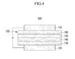
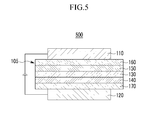
- FIGS. 1 to 5 are cross-sectional views showing organic photoelectric devices including the compound for an organic photoelectric device.
- the organic photoelectric devices 100, 200, 300, 400, and 500 includes at least one organic thin layer 105 interposed between an anode 120 and a cathode 110.
- a substrate of an organic photoelectric device is not particularly limited in the related arts, but a glass substrate or a transparent plastic substrate having excellent transparency, surface smoothness, handling ease, and water repellency.
- the anode 120 includes an anode material laving a large work function to help hole injection into an organic thin layer.
- the anode material includes a metal such as nickel, platinum, vanadium, chromium, copper, zinc, gold, and the like or an alloy of the foregoing metals; metal oxide such as zinc oxide, indium oxide, indium tin oxide (ITO), indium zinc oxide (IZO), and the like; a combined metal and oxide such as ZnO/Al, SnO 2 /Sb, and the like.
- the anode material is not limited thereto.
- the anode material may be a transparent electrode including ITO.
- the cathode 110 includes a cathode material having a small work function to help electron injection into an organic thin layer.
- the cathode material includes a metal such as magnesium, calcium, sodium, potassium, titanium, indium, yttrium, lithium, gadolinium, aluminum, silver, tin, lead, cesium, barium, and the metal, or alloys thereof; or a multi-layered material such as LiF/Al, LiO 2 /Al, LiF/Ca, LiF/Al, BaF 2 /Ca, and the like.
- the cathode material is not limited to the above materials.
- the cathode material may be a metal electrode such as aluminum.
- the organic photoelectric device 100 includes an organic thin layer 105 including only an emission layer 130.
- a double-layered organic photoelectric device 200 includes an organic thin layer 105 including an emission layer 230 including an electron transport layer (ETL), and a hole transport layer (HTL) 140.
- the emission layer 130 also functions as an electron transport layer (ETL), and the hole transport layer (HTL) 140 layer has an excellent binding property with a transparent electrode such as ITO or an excellent hole transporting property.
- the hole transport layer (HTL) 140 may include generally-used hole transport material without limitation, for example poly (3,4-ethylenedioxy-thiophene) (PEDOT) doped with poly(styrenesulfonate) (PSS) (PEDOT:PSS), N,N'-bis (3-methylphenyl)-N,N-diphenyl-[1,1'-biphenyl]-4,4'-diamine (TPD), N,N'-di (1-naphthyl)-N,N'-diphenylbenzidine (NPB) and the like, along with the compound for an organic photoelectric device according to one embodiment of the present invention.
- the hole transport material is not limited to the above materials.
- a three-layered organic photoelectric device 300 includes an organic thin layer 105 including an electron transport layer (ETL) 150, an emission layer 130, and a hole transport layer (HTL) 140.
- the emission layer 130 is independently installed, and layers having an excellent electron transporting property or an excellent hole transporting property are separately stacked.
- the electron transport layer (ETL) 150 may include generally-used electron transport material without limitation, for example, aluminum tris(8-hydroxyquinoline) (Alq 3 ); a 1,3,4-oxadiazole derivative such as 2-(4-biphenyl-5-phenyl-1,3,4-oxadiazole (PBD); a quinoxalin derivative such as 1,3,4-tris[(3-phenyl-6-trifluoromethyl) quinoxalin-2-yl]benzene (TPQ); and a triazole derivative, along with the compound for an organic photoelectric device according to one embodiment of the present invention.
- the electron transport material is not limited to the above materials.
- FIG. 4 shows a four-layered organic photoelectric device 400 that includes an organic thin layer 105 including an electron injection layer (EIL) 160, an emission layer 130, a hole transport layer (HTL) 140, and a hole injection layer (HIL) 170 for binding with the cathode of ITO.
- EIL electron injection layer
- HTL hole transport layer
- HIL hole injection layer
- FIG. 5 shows a five layered organic photoelectric device 500 that includes an organic thin layer 105 including an electron transport layer (ETL) 150, an emission layer 130, a hole transport layer (HTL) 140, and a hole injection layer (HIL) 170, and further includes an electron injection layer (EIL) 160 to achieve a low voltage.
- ETL electron transport layer
- HTL hole transport layer
- HIL hole injection layer
- the emission layers 130 and 230 may have a thickness of 5 to 1000 nm
- the hole transport layer (HTL) 140 and electron transport layer (ETL) 150 may have a thickness of 10 to 10,000 ⁇ , respectively.
- the thicknesses are not limited to the above range.
- the organic thin layer 105 selected from the electron transport layer (ETL) 150, electron injection layer (EIL) 160, emission layer 130 and 230, hole transport layer (HTL) 140, hole injection layer (HIL) 170 and a combination thereof includes the compound for an organic photoelectric device according to one embodiment.
- the material for the organic photoelectric device may be used for an electron transport layer (ETL) 150 including the electron transport layer (ETL) 150 or electron injection layer (EIL) 160.
- ETL electron transport layer
- EIL electron injection layer
- the material for the organic photoelectric device may be included as a phosphorescent host, and the emission layer 130 and 230 may further include a dopant.
- the dopant may be a red, green and blue, or white phosphorescent dopant.
- the organic photoelectric device may be fabricated by: forming an anode on a substrate, forming an organic thin layer in accordance with a dry coating method such as evaporation, sputtering, plasma plating, and ion plating, or a wet coating method such as spin coating, dipping, and flow coating; and providing a cathode thereon.
- a dry coating method such as evaporation, sputtering, plasma plating, and ion plating
- a wet coating method such as spin coating, dipping, and flow coating
- Another embodiment of the present invention provides a display device including the organic photoelectric device.
- a compound for an organic photoelectric device was synthesized according to the following reaction scheme 1.
- the agitated reactant was cooled down to a room temperature to complete the reaction and then, extracted with methylene chloride and cleaned with water. Next, the reactant was treated with anhydrous magnesium sulfate to remove moisture and filtrated to remove an organic solvent therein. The final residue was purified through silica gel chromatography using a mixed solvent prepared by mixing methylene chloride and hexane in a volume ratio of 1:1, obtaining 9 g of an intermediate product (B) (a yield: 82.7 %).
- the reactant was extracted with methylenechloride and cleaned with water, after the organic solvent therein was distillated and removed under reduced pressure. Then, the reactant was treated with anhydrous magnesium sulfate to remove moisture and filtrated to remove an organic solvent therein. The final residue was purified through silica gel chromatography using a mixed solvent prepared by mixing methylenechloride and hexane in a volume ratio of 2:1, obtaining 5.3 g of an intermediate product (C) (a yield: 71.5 %).
- the agitated reactant was cooled down to a room temperature to complete the reaction and then, extracted with methylene chloride and cleaned with water. Then, the resulting reactant was treated with anhydrous magnesium sulfate to remove moisture and filtrated to remove an organic solvent therein. The final residue was purified and recrystallized through silica gel chromatography using a mixed solvent prepared by mixing methylene chloride and hexane in a volume ratio of 1:3, obtaining 4 g of a compound for an organic photoelectric device (a yield: 51.3 %).
- a compound for an organic photoelectric device was synthesized according to the following reaction scheme 2.
- the resulting reactant was cooled down to a room temperature to complete the reaction and then, extracted with methylene chloride and cleaned with water. Then, the reactant was treated with anhydrous magnesium sulfate and filtrated to remove an organic solvent therein. The final residue was purified through silica gel chromatography using a mixed solvent prepared by mixing methylenechloride and hexane in a volume ratio of 1:1, obtaining 7 g of an intermediate product (E) (a yield: 72 %).
- the reactant was distillated to remove an organic solvent under a reduced pressure and then, extracted with methylene chloride and cleaned with water. Next, the reactant was treated with anhydrous magnesium sulfate to remove moisture and filtrated to remove an organic solvent therein. The final residue was purified through silica gel chromatography using a mixed solvent prepared by mixing methylenechloride and hexane in a volume ratio of 2:1, obtaining 4.3 g of an intermediate product (F) (a yield: 65.9 %).
- the mixture was agitated for 30 minutes. Then, the mixture was further agitated at a room temperature for 20 minutes, and 2.43 g (9.09 mmol) of 2-chloro-4,6-diphenyl triazine was added thereto at -78 °C. The mixture was agitated at a room temperature for 12 minutes.
- the reactant was cooled down to a room temperature to complete the reaction and then, extracted with methylene chloride and cleaned with water. Then, the reactant was treated with anhydrous magnesium sulfate to remove moisture and filtrated to remove an organic solvent therein. The final residue was purified and recrystallized through silica gel chromatography using a mixed solvent prepared by mixing methylenechloride and hexane in a volume ratio of 1:3, obtaining 3.2 g of a compound for an organic photoelectric device (a yield: 54.1 %).
- ITO was formed to be 1000 ⁇ thick as an anode
- aluminum (AI) was formed to be 1500 ⁇ thick as a cathode.
- an anode for an organic light emitting diode was fabricated by cutting an ITO glass substrate with 15 ⁇ /cm 2 of sheet resistance to have a size of 50 mm ⁇ 50 mm ⁇ 0.7 mm and then, ultrasonic wave cleaning it in acetone and isopropyl alcohol and pure water respectively for 15 minutes and UV ozone-cleaning it for 30 minutes.
- a 800 A hole transport layer was formed by depositing N,N'-di(1-naphthyl)-N,N'-diphenylbenzidine (NPB) (70 nm) and 4,4',4"-tri(N-carbazolyl)triphenylamine (TCTA) (10 nm) with a vacuum degree of 650 ⁇ 10 -7 Pa at a deposit speed ranging from 0.1 to 0.3 nm/s.
- NPB N,N'-di(1-naphthyl)-N,N'-diphenylbenzidine
- TCTA 4,4',4"-tri(N-carbazolyl)triphenylamine
- a 300 A-thick emission layer was formed by using the compound synthesized according to Example 1 under the same vacuum deposition condition, and a phosphorescent dopant, Ir(PPy) 3 , was simultaneously deposited.
- the phosphorescence dopant was deposited in an amount of 7 wt% based on 100 wt% of the total weight of the emission layer by regulating its deposition speed.
- a 50 A-thick hole-blocking layer was formed by depositing bis(8-hydroxy-2-methylquinolinato)-aluminumbiphenoxide (BAlq) under the same vacuum deposition condition.
- ETL electron transport layer
- the organic light emitting diode had a structure of ITO/ NPB (70 nm)/ TCTA (10 nm)/ EML (the compound (93 wt%) of Example 1 + Ir(PPy) 3 (7 wt%), 30 nm)/ Balq (5 nm)/ Alq 3 (20 nm)/ LiF (0.5 nm) / Al (150 nm).
- An organic light emitting diode was fabricated according to the same method as Example 3 except for using 4,4-N,N-dicarbazolebiphenyl (CBP) as a host for an emission layer instead of the compound of Example 1.
- CBP 4,4-N,N-dicarbazolebiphenyl
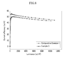
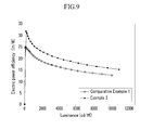
- Example 3 and Comparative Example 1 were measured regarding current density change and luminance change depending on voltage and luminous efficiency.
- the current density change and luminance change depending on voltage and luminous efficiency were measured in the following method. The results are provided in the following Table 1.
- the organic light emitting diodes were measured regarding current using a current-voltage meter (Keithley 2400) while their voltages were increased from 0 V to 10 V. The results are provided in FIG. 6 .
- the organic light emitting diodes were measured regarding luminance using a luminance meter (Minolta Cs-1000A), while their voltages were increased from 0 V to 10 V. The results are provided in FIG. 7 .
- the organic light emitting diodes were measured regarding color coordinate using a luminance meter (Minolta Cs-100A). The results are provided in the following Table 1. (Table 1) Device Host material of emission layer at 2000 cd/m 2 Driving voltage (V) Current efficiency (cd/A) Electric power efficiency (Im/W) Color coordinate (x,y) Example 3 Example 1 7.2 51.8 22.6 0.308, 0.622 Comparative Example 1 CBP 8.2 49.2 18.8 0.295, 0.622
- the organic light emitting diode of Example 3 had about 1 V lower driving voltage than the one of Comparative Example 1 and very improved current efficiency and electric power efficiency compared therewith. Accordingly, the compound according to Example 1 was identified to lower driving voltage and to improve luminance and efficiency of an organic light emitting diode.
Landscapes
- Chemical & Material Sciences (AREA)
- Organic Chemistry (AREA)
- Engineering & Computer Science (AREA)
- Materials Engineering (AREA)
- Physics & Mathematics (AREA)
- Spectroscopy & Molecular Physics (AREA)
- Manufacturing & Machinery (AREA)
- Electroluminescent Light Sources (AREA)
- Plural Heterocyclic Compounds (AREA)
Applications Claiming Priority (2)
| Application Number | Priority Date | Filing Date | Title |
|---|---|---|---|
| KR20090057234A KR101333694B1 (ko) | 2009-06-25 | 2009-06-25 | 유기광전소자용 화합물 및 이를 포함하는 유기광전소자 |
| PCT/KR2010/004156 WO2010151083A2 (ko) | 2009-06-25 | 2010-06-25 | 유기광전소자용 화합물 및 이를 포함하는 유기광전소자 |
Publications (3)
| Publication Number | Publication Date |
|---|---|
| EP2447334A2 true EP2447334A2 (de) | 2012-05-02 |
| EP2447334A4 EP2447334A4 (de) | 2013-01-02 |
| EP2447334B1 EP2447334B1 (de) | 2014-09-17 |
Family
ID=43387072
Family Applications (1)
| Application Number | Title | Priority Date | Filing Date |
|---|---|---|---|
| EP20100792365 Active EP2447334B1 (de) | 2009-06-25 | 2010-06-25 | Verbindung für ein organisches photoelektrisches element und organisches photoelektrisches element damit |
Country Status (6)
| Country | Link |
|---|---|
| US (1) | US9017827B2 (de) |
| EP (1) | EP2447334B1 (de) |
| JP (1) | JP5746162B2 (de) |
| KR (1) | KR101333694B1 (de) |
| CN (1) | CN102459507B (de) |
| WO (1) | WO2010151083A2 (de) |
Cited By (3)
| Publication number | Priority date | Publication date | Assignee | Title |
|---|---|---|---|---|
| WO2015170930A1 (en) * | 2014-05-08 | 2015-11-12 | Rohm And Haas Electronic Materials Korea Ltd. | An electron transport material and an organic electroluminescence device comprising the same |
| WO2017094458A1 (ja) | 2015-11-30 | 2017-06-08 | 日本化学工業株式会社 | 電気化学発光セル、電気化学発光セルの発光層形成用組成物、及び電気化学発光セルの発光層用イオン性化合物 |
| EP4520758A4 (de) * | 2022-06-02 | 2026-04-01 | Sfc Co Ltd | Organische verbindung und organische lichtemittierende vorrichtung damit |
Families Citing this family (20)
| Publication number | Priority date | Publication date | Assignee | Title |
|---|---|---|---|---|
| DE102009031021A1 (de) * | 2009-06-30 | 2011-01-05 | Merck Patent Gmbh | Materialien für organische Elektrolumineszenzvorrichtungen |
| KR20110009920A (ko) * | 2009-07-23 | 2011-01-31 | 다우어드밴스드디스플레이머티리얼 유한회사 | 신규한 유기 발광 화합물 및 이를 포함하는 유기 전계 발광 소자 |
| US8586206B2 (en) * | 2010-06-30 | 2013-11-19 | Idemitsu Kosan Co., Ltd. | Aromatic amine derivative and organic electroluminescence device using the same |
| KR101832171B1 (ko) * | 2010-10-25 | 2018-04-16 | 삼성디스플레이 주식회사 | 축합환 화합물, 이를 포함한 유기 발광 소자 및 상기 유기 발광 소자를 포함한 평판 표시 장치 |
| US20130306961A1 (en) * | 2011-02-11 | 2013-11-21 | Idemitsu Kosen Co. Ltd | Organic light emitting device and materials for use in same |
| KR20130015400A (ko) * | 2011-08-03 | 2013-02-14 | 삼성디스플레이 주식회사 | 헤테로고리 화합물 및 이를 포함하는 유기 전계 발광 소자 |
| KR102054229B1 (ko) * | 2012-01-13 | 2019-12-11 | 덕산네오룩스 주식회사 | 유기전기 소자용 화합물, 이를 이용한 유기전기소자 및 그 전자 장치 |
| EP2935276B1 (de) * | 2012-12-21 | 2017-11-01 | Merck Patent GmbH | Materialien für organische elektrolumineszenzvorrichtungen |
| KR101577104B1 (ko) | 2012-12-28 | 2015-12-14 | 주식회사 두산 | 유기 화합물 및 이를 포함하는 유기 전계 발광 소자 |
| KR102120894B1 (ko) * | 2013-05-03 | 2020-06-10 | 삼성디스플레이 주식회사 | 유기 발광 소자 |
| KR101627743B1 (ko) * | 2013-08-07 | 2016-06-07 | 제일모직 주식회사 | 화합물, 이를 포함하는 발광 재료, 유기 광전자 소자 및 상기 유기 광전자 소자를 포함하는 표시장치 |
| KR102411748B1 (ko) * | 2014-03-17 | 2022-06-23 | 롬엔드하스전자재료코리아유한회사 | 전자 버퍼 재료 및 유기 전계 발광 소자 |
| JP6163185B2 (ja) | 2014-10-09 | 2017-07-12 | 日本化学工業株式会社 | 電気化学発光セル及び電気化学発光セルの発光層形成用組成物 |
| KR102417121B1 (ko) * | 2014-10-17 | 2022-07-06 | 삼성디스플레이 주식회사 | 유기 발광 소자 |
| KR101818581B1 (ko) * | 2014-10-31 | 2018-01-15 | 삼성에스디아이 주식회사 | 유기 광전자 소자 및 표시 장치 |
| KR102432080B1 (ko) * | 2014-12-08 | 2022-08-16 | 엘지디스플레이 주식회사 | 유기전계발광소자 |
| EP3032605B1 (de) | 2014-12-08 | 2019-08-21 | LG Display Co., Ltd. | Organische lichtemittierende anzeigevorrichtung |
| JP5994038B1 (ja) * | 2014-12-12 | 2016-09-21 | 日本化学工業株式会社 | 電気化学発光セル、電気化学発光セルの発光層形成用組成物、及び電気化学発光セルの発光層用イオン性化合物 |
| CN108203403A (zh) * | 2016-12-20 | 2018-06-26 | 武汉尚赛光电科技有限公司 | 具有热致延迟荧光的发光材料、其应用及电致发光器件 |
| CN119899175B (zh) * | 2024-12-16 | 2025-12-05 | 阜阳欣奕华新材料科技股份有限公司 | 三嗪类化合物、有机电致发光器件、显示装置 |
Family Cites Families (14)
| Publication number | Priority date | Publication date | Assignee | Title |
|---|---|---|---|---|
| EP0765106B1 (de) * | 1995-09-25 | 2002-11-27 | Toyo Ink Manufacturing Co., Ltd. | Leuchtemittierender Stoff für organische Elektrolumineszensvorrichtung, und organische Elektrolumineszensvorrichtung mit diesem leuchtemittierendem dafür geeignetem Stoff |
| US5952115A (en) * | 1997-10-02 | 1999-09-14 | Xerox Corporation | Electroluminescent devices |
| US5942340A (en) * | 1997-10-02 | 1999-08-24 | Xerox Corporation | Indolocarbazole electroluminescent devices |
| US7485376B2 (en) * | 2003-03-26 | 2009-02-03 | Konica Minolta Holdings, Inc. | Organic electroluminescent element, illuminator, and display |
| KR101030010B1 (ko) * | 2004-09-18 | 2011-04-20 | 삼성모바일디스플레이주식회사 | 청색 발광 고분자 및 이를 채용한 유기 전계 발광 소자 |
| KR101146976B1 (ko) | 2005-01-06 | 2012-05-23 | 삼성모바일디스플레이주식회사 | 청색 발광 고분자 및 이를 채용한 유기 전계 발광 소자 |
| KR101156529B1 (ko) | 2005-10-18 | 2012-06-20 | 삼성에스디아이 주식회사 | 신규한 홀 전달물질 및 이를 이용한 고체전해질 및광전변환소자 |
| DE102006031990A1 (de) | 2006-07-11 | 2008-01-17 | Merck Patent Gmbh | Neue Materialien für organische Elektrolumineszenzvorrichtungen |
| US8062769B2 (en) * | 2006-11-09 | 2011-11-22 | Nippon Steel Chemical Co., Ltd. | Indolocarbazole compound for use in organic electroluminescent device and organic electroluminescent device |
| KR20080047209A (ko) * | 2006-11-24 | 2008-05-28 | 삼성전자주식회사 | 유기 발광 화합물 및 이를 구비한 유기 발광 소자 |
| DE102008017591A1 (de) * | 2008-04-07 | 2009-10-08 | Merck Patent Gmbh | Neue Materialien für organische Elektrolumineszenzvorrichtungen |
| KR101026171B1 (ko) * | 2008-07-01 | 2011-04-05 | 덕산하이메탈(주) | 신규의 축합 카바졸 유도체 및 이를 포함하는 유기전계발광 소자 |
| DE102009005288A1 (de) * | 2009-01-20 | 2010-07-22 | Merck Patent Gmbh | Materialien für organische Elektrolumineszenzvorrichtungen |
| DE102009023155A1 (de) * | 2009-05-29 | 2010-12-02 | Merck Patent Gmbh | Materialien für organische Elektrolumineszenzvorrichtungen |
-
2009
- 2009-06-25 KR KR20090057234A patent/KR101333694B1/ko active Active
-
2010
- 2010-06-25 CN CN201080026243.2A patent/CN102459507B/zh active Active
- 2010-06-25 JP JP2012517398A patent/JP5746162B2/ja active Active
- 2010-06-25 WO PCT/KR2010/004156 patent/WO2010151083A2/ko not_active Ceased
- 2010-06-25 EP EP20100792365 patent/EP2447334B1/de active Active
-
2011
- 2011-12-23 US US13/336,019 patent/US9017827B2/en active Active
Cited By (4)
| Publication number | Priority date | Publication date | Assignee | Title |
|---|---|---|---|---|
| WO2015170930A1 (en) * | 2014-05-08 | 2015-11-12 | Rohm And Haas Electronic Materials Korea Ltd. | An electron transport material and an organic electroluminescence device comprising the same |
| WO2017094458A1 (ja) | 2015-11-30 | 2017-06-08 | 日本化学工業株式会社 | 電気化学発光セル、電気化学発光セルの発光層形成用組成物、及び電気化学発光セルの発光層用イオン性化合物 |
| US10930872B2 (en) | 2015-11-30 | 2021-02-23 | Nippon Chemical Industrial Co., Ltd. | Light-emitting electrochemical cell, composition for forming light-emitting layer of light-emitting electrochemical cell, and ionic compound for light-emitting layer of light-emitting electrochemical cell |
| EP4520758A4 (de) * | 2022-06-02 | 2026-04-01 | Sfc Co Ltd | Organische verbindung und organische lichtemittierende vorrichtung damit |
Also Published As
| Publication number | Publication date |
|---|---|
| EP2447334A4 (de) | 2013-01-02 |
| KR20100138630A (ko) | 2010-12-31 |
| JP5746162B2 (ja) | 2015-07-08 |
| WO2010151083A2 (ko) | 2010-12-29 |
| CN102459507A (zh) | 2012-05-16 |
| EP2447334B1 (de) | 2014-09-17 |
| US20120091446A1 (en) | 2012-04-19 |
| JP2012531737A (ja) | 2012-12-10 |
| US9017827B2 (en) | 2015-04-28 |
| CN102459507B (zh) | 2015-07-22 |
| KR101333694B1 (ko) | 2013-11-27 |
| WO2010151083A3 (ko) | 2011-04-14 |
Similar Documents
| Publication | Publication Date | Title |
|---|---|---|
| EP2447334B1 (de) | Verbindung für ein organisches photoelektrisches element und organisches photoelektrisches element damit | |
| EP2447335B1 (de) | Verbindung für ein organisches photoelektrisches element und organisches photoelektrisches element damit | |
| EP2431445B1 (de) | Verbindung für organische photoelektrische vorrichtung und organische photoelektrische vorrichtung damit | |
| EP3460024B1 (de) | Verbindung für eine organische photoelektrische vorrichtung und organische photoelektrische vorrichtung damit | |
| EP2376594B1 (de) | Verbindung für eine organische photoelektrische vorrichtung sowie sie enthaltende organische photoelektrische vorrichtung | |
| TWI471406B (zh) | A phosphorescent element, and an organic electroluminescent device using the same | |
| CN103732603B (zh) | 包含氮杂苯并咪唑碳烯配体的金属配合物及其在oled中的用途 | |
| EP2315753B1 (de) | Material für eine organische photoelektrische vorrichtung und organische photoelektrische vorrichtung damit | |
| EP2452997A2 (de) | Verbindung für ein organisches photoelektrisches element und organisches photoelektrisches element damit | |
| KR101247626B1 (ko) | 유기광전소자용 화합물 및 이를 포함하는 유기광전소자 | |
| EP2383323A2 (de) | Neue verbindungen für eine organische photoelektrische vorrichtung sowie sie enthaltende organische photoelektrische vorrichtung | |
| KR20150111271A (ko) | 신규한 유기발광화합물 및 이를 포함하는 유기 발광 소자 | |
| KR20100075079A (ko) | 신규한 유기광전소자용 화합물 및 이를 포함하는 유기광전소자 | |
| TWI483936B (zh) | 用於有機光電元件之新穎化合物及包括該化合物之有機光電元件 | |
| JP2008120696A (ja) | 新規なトリピリジルフェニル誘導体、それよりなる電子輸送材料およびそれを含む有機エレクトロルミネッセンス素子 | |
| WO2014104545A1 (ko) | 유기광전자소자용 화합물, 이를 포함하는 유기발광소자 및 상기 유기발광소자를 포함하는 표시장치 | |
| KR20150064687A (ko) | 신규한 청색 형광 호스트 화합물 및 이를 포함하는 유기발광소자 | |
| JP2009126793A (ja) | 新規なジ(ピリジルフェニル)誘導体、それよりなる電子輸送材料およびそれを含む有機エレクトロルミネッセンス素子 | |
| KR20100121267A (ko) | 유기광전소자용 화합물 및 이를 포함하는 유기광전소자 | |
| KR20150124924A (ko) | 신규한 화합물 및 이를 포함하는 유기발광소자 | |
| Pei et al. | Highly twisted organic molecules with ortho linkage as the efficient bipolar hosts for sky-blue thermally activated delayed fluorescence emitter in OLEDs | |
| JP5001914B2 (ja) | ビスホスフィンジオキサイド誘導体よりなるホスト材料およびビスホスフィンジオキサイド誘導体を含有する有機エレクトロルミネッセンス素子 | |
| CN101331145A (zh) | 金属配位化合物以及应用该化合物的有机电致发光元件 |
Legal Events
| Date | Code | Title | Description |
|---|---|---|---|
| PUAI | Public reference made under article 153(3) epc to a published international application that has entered the european phase |
Free format text: ORIGINAL CODE: 0009012 |
|
| 17P | Request for examination filed |
Effective date: 20111128 |
|
| AK | Designated contracting states |
Kind code of ref document: A2 Designated state(s): AL AT BE BG CH CY CZ DE DK EE ES FI FR GB GR HR HU IE IS IT LI LT LU LV MC MK MT NL NO PL PT RO SE SI SK SM TR |
|
| DAX | Request for extension of the european patent (deleted) | ||
| A4 | Supplementary search report drawn up and despatched |
Effective date: 20121204 |
|
| RIC1 | Information provided on ipc code assigned before grant |
Ipc: H05B 33/14 20060101ALI20121128BHEP Ipc: H05B 33/10 20060101ALI20121128BHEP Ipc: C09K 11/06 20060101AFI20121128BHEP |
|
| GRAP | Despatch of communication of intention to grant a patent |
Free format text: ORIGINAL CODE: EPIDOSNIGR1 |
|
| INTG | Intention to grant announced |
Effective date: 20140416 |
|
| GRAS | Grant fee paid |
Free format text: ORIGINAL CODE: EPIDOSNIGR3 |
|
| GRAA | (expected) grant |
Free format text: ORIGINAL CODE: 0009210 |
|
| AK | Designated contracting states |
Kind code of ref document: B1 Designated state(s): AL AT BE BG CH CY CZ DE DK EE ES FI FR GB GR HR HU IE IS IT LI LT LU LV MC MK MT NL NO PL PT RO SE SI SK SM TR |
|
| REG | Reference to a national code |
Ref country code: GB Ref legal event code: FG4D |
|
| REG | Reference to a national code |
Ref country code: CH Ref legal event code: EP |
|
| REG | Reference to a national code |
Ref country code: IE Ref legal event code: FG4D |
|
| REG | Reference to a national code |
Ref country code: AT Ref legal event code: REF Ref document number: 687716 Country of ref document: AT Kind code of ref document: T Effective date: 20141015 |
|
| REG | Reference to a national code |
Ref country code: DE Ref legal event code: R096 Ref document number: 602010019046 Country of ref document: DE Effective date: 20141030 |
|
| REG | Reference to a national code |
Ref country code: NL Ref legal event code: T3 |
|
| PG25 | Lapsed in a contracting state [announced via postgrant information from national office to epo] |
Ref country code: LT Free format text: LAPSE BECAUSE OF FAILURE TO SUBMIT A TRANSLATION OF THE DESCRIPTION OR TO PAY THE FEE WITHIN THE PRESCRIBED TIME-LIMIT Effective date: 20140917 Ref country code: SE Free format text: LAPSE BECAUSE OF FAILURE TO SUBMIT A TRANSLATION OF THE DESCRIPTION OR TO PAY THE FEE WITHIN THE PRESCRIBED TIME-LIMIT Effective date: 20140917 Ref country code: NO Free format text: LAPSE BECAUSE OF FAILURE TO SUBMIT A TRANSLATION OF THE DESCRIPTION OR TO PAY THE FEE WITHIN THE PRESCRIBED TIME-LIMIT Effective date: 20141217 Ref country code: GR Free format text: LAPSE BECAUSE OF FAILURE TO SUBMIT A TRANSLATION OF THE DESCRIPTION OR TO PAY THE FEE WITHIN THE PRESCRIBED TIME-LIMIT Effective date: 20141218 Ref country code: FI Free format text: LAPSE BECAUSE OF FAILURE TO SUBMIT A TRANSLATION OF THE DESCRIPTION OR TO PAY THE FEE WITHIN THE PRESCRIBED TIME-LIMIT Effective date: 20140917 |
|
| REG | Reference to a national code |
Ref country code: LT Ref legal event code: MG4D |
|
| PG25 | Lapsed in a contracting state [announced via postgrant information from national office to epo] |
Ref country code: HR Free format text: LAPSE BECAUSE OF FAILURE TO SUBMIT A TRANSLATION OF THE DESCRIPTION OR TO PAY THE FEE WITHIN THE PRESCRIBED TIME-LIMIT Effective date: 20140917 Ref country code: LV Free format text: LAPSE BECAUSE OF FAILURE TO SUBMIT A TRANSLATION OF THE DESCRIPTION OR TO PAY THE FEE WITHIN THE PRESCRIBED TIME-LIMIT Effective date: 20140917 Ref country code: CY Free format text: LAPSE BECAUSE OF FAILURE TO SUBMIT A TRANSLATION OF THE DESCRIPTION OR TO PAY THE FEE WITHIN THE PRESCRIBED TIME-LIMIT Effective date: 20140917 |
|
| REG | Reference to a national code |
Ref country code: AT Ref legal event code: MK05 Ref document number: 687716 Country of ref document: AT Kind code of ref document: T Effective date: 20140917 |
|
| PG25 | Lapsed in a contracting state [announced via postgrant information from national office to epo] |
Ref country code: CZ Free format text: LAPSE BECAUSE OF FAILURE TO SUBMIT A TRANSLATION OF THE DESCRIPTION OR TO PAY THE FEE WITHIN THE PRESCRIBED TIME-LIMIT Effective date: 20140917 Ref country code: RO Free format text: LAPSE BECAUSE OF FAILURE TO SUBMIT A TRANSLATION OF THE DESCRIPTION OR TO PAY THE FEE WITHIN THE PRESCRIBED TIME-LIMIT Effective date: 20140917 Ref country code: EE Free format text: LAPSE BECAUSE OF FAILURE TO SUBMIT A TRANSLATION OF THE DESCRIPTION OR TO PAY THE FEE WITHIN THE PRESCRIBED TIME-LIMIT Effective date: 20140917 Ref country code: SK Free format text: LAPSE BECAUSE OF FAILURE TO SUBMIT A TRANSLATION OF THE DESCRIPTION OR TO PAY THE FEE WITHIN THE PRESCRIBED TIME-LIMIT Effective date: 20140917 Ref country code: IS Free format text: LAPSE BECAUSE OF FAILURE TO SUBMIT A TRANSLATION OF THE DESCRIPTION OR TO PAY THE FEE WITHIN THE PRESCRIBED TIME-LIMIT Effective date: 20150117 Ref country code: PT Free format text: LAPSE BECAUSE OF FAILURE TO SUBMIT A TRANSLATION OF THE DESCRIPTION OR TO PAY THE FEE WITHIN THE PRESCRIBED TIME-LIMIT Effective date: 20150119 Ref country code: ES Free format text: LAPSE BECAUSE OF FAILURE TO SUBMIT A TRANSLATION OF THE DESCRIPTION OR TO PAY THE FEE WITHIN THE PRESCRIBED TIME-LIMIT Effective date: 20140917 |
|
| PG25 | Lapsed in a contracting state [announced via postgrant information from national office to epo] |
Ref country code: PL Free format text: LAPSE BECAUSE OF FAILURE TO SUBMIT A TRANSLATION OF THE DESCRIPTION OR TO PAY THE FEE WITHIN THE PRESCRIBED TIME-LIMIT Effective date: 20140917 Ref country code: AT Free format text: LAPSE BECAUSE OF FAILURE TO SUBMIT A TRANSLATION OF THE DESCRIPTION OR TO PAY THE FEE WITHIN THE PRESCRIBED TIME-LIMIT Effective date: 20140917 |
|
| REG | Reference to a national code |
Ref country code: DE Ref legal event code: R097 Ref document number: 602010019046 Country of ref document: DE |
|
| PLBE | No opposition filed within time limit |
Free format text: ORIGINAL CODE: 0009261 |
|
| STAA | Information on the status of an ep patent application or granted ep patent |
Free format text: STATUS: NO OPPOSITION FILED WITHIN TIME LIMIT |
|
| PG25 | Lapsed in a contracting state [announced via postgrant information from national office to epo] |
Ref country code: DK Free format text: LAPSE BECAUSE OF FAILURE TO SUBMIT A TRANSLATION OF THE DESCRIPTION OR TO PAY THE FEE WITHIN THE PRESCRIBED TIME-LIMIT Effective date: 20140917 |
|
| 26N | No opposition filed |
Effective date: 20150618 |
|
| PG25 | Lapsed in a contracting state [announced via postgrant information from national office to epo] |
Ref country code: IT Free format text: LAPSE BECAUSE OF FAILURE TO SUBMIT A TRANSLATION OF THE DESCRIPTION OR TO PAY THE FEE WITHIN THE PRESCRIBED TIME-LIMIT Effective date: 20140917 |
|
| PG25 | Lapsed in a contracting state [announced via postgrant information from national office to epo] |
Ref country code: SI Free format text: LAPSE BECAUSE OF FAILURE TO SUBMIT A TRANSLATION OF THE DESCRIPTION OR TO PAY THE FEE WITHIN THE PRESCRIBED TIME-LIMIT Effective date: 20140917 |
|
| PG25 | Lapsed in a contracting state [announced via postgrant information from national office to epo] |
Ref country code: MC Free format text: LAPSE BECAUSE OF FAILURE TO SUBMIT A TRANSLATION OF THE DESCRIPTION OR TO PAY THE FEE WITHIN THE PRESCRIBED TIME-LIMIT Effective date: 20140917 |
|
| REG | Reference to a national code |
Ref country code: CH Ref legal event code: PL |
|
| GBPC | Gb: european patent ceased through non-payment of renewal fee |
Effective date: 20150625 |
|
| PG25 | Lapsed in a contracting state [announced via postgrant information from national office to epo] |
Ref country code: LU Free format text: LAPSE BECAUSE OF FAILURE TO SUBMIT A TRANSLATION OF THE DESCRIPTION OR TO PAY THE FEE WITHIN THE PRESCRIBED TIME-LIMIT Effective date: 20150625 |
|
| REG | Reference to a national code |
Ref country code: IE Ref legal event code: MM4A |
|
| REG | Reference to a national code |
Ref country code: FR Ref legal event code: ST Effective date: 20160229 |
|
| PG25 | Lapsed in a contracting state [announced via postgrant information from national office to epo] |
Ref country code: CH Free format text: LAPSE BECAUSE OF NON-PAYMENT OF DUE FEES Effective date: 20150630 Ref country code: IE Free format text: LAPSE BECAUSE OF NON-PAYMENT OF DUE FEES Effective date: 20150625 Ref country code: LI Free format text: LAPSE BECAUSE OF NON-PAYMENT OF DUE FEES Effective date: 20150630 Ref country code: GB Free format text: LAPSE BECAUSE OF NON-PAYMENT OF DUE FEES Effective date: 20150625 |
|
| PG25 | Lapsed in a contracting state [announced via postgrant information from national office to epo] |
Ref country code: FR Free format text: LAPSE BECAUSE OF NON-PAYMENT OF DUE FEES Effective date: 20150630 |
|
| PG25 | Lapsed in a contracting state [announced via postgrant information from national office to epo] |
Ref country code: MT Free format text: LAPSE BECAUSE OF FAILURE TO SUBMIT A TRANSLATION OF THE DESCRIPTION OR TO PAY THE FEE WITHIN THE PRESCRIBED TIME-LIMIT Effective date: 20140917 |
|
| PG25 | Lapsed in a contracting state [announced via postgrant information from national office to epo] |
Ref country code: HU Free format text: LAPSE BECAUSE OF FAILURE TO SUBMIT A TRANSLATION OF THE DESCRIPTION OR TO PAY THE FEE WITHIN THE PRESCRIBED TIME-LIMIT; INVALID AB INITIO Effective date: 20100625 Ref country code: SM Free format text: LAPSE BECAUSE OF FAILURE TO SUBMIT A TRANSLATION OF THE DESCRIPTION OR TO PAY THE FEE WITHIN THE PRESCRIBED TIME-LIMIT Effective date: 20140917 Ref country code: BG Free format text: LAPSE BECAUSE OF FAILURE TO SUBMIT A TRANSLATION OF THE DESCRIPTION OR TO PAY THE FEE WITHIN THE PRESCRIBED TIME-LIMIT Effective date: 20140917 |
|
| PG25 | Lapsed in a contracting state [announced via postgrant information from national office to epo] |
Ref country code: TR Free format text: LAPSE BECAUSE OF FAILURE TO SUBMIT A TRANSLATION OF THE DESCRIPTION OR TO PAY THE FEE WITHIN THE PRESCRIBED TIME-LIMIT Effective date: 20140917 |
|
| PG25 | Lapsed in a contracting state [announced via postgrant information from national office to epo] |
Ref country code: BE Free format text: LAPSE BECAUSE OF FAILURE TO SUBMIT A TRANSLATION OF THE DESCRIPTION OR TO PAY THE FEE WITHIN THE PRESCRIBED TIME-LIMIT Effective date: 20140917 |
|
| PG25 | Lapsed in a contracting state [announced via postgrant information from national office to epo] |
Ref country code: MK Free format text: LAPSE BECAUSE OF FAILURE TO SUBMIT A TRANSLATION OF THE DESCRIPTION OR TO PAY THE FEE WITHIN THE PRESCRIBED TIME-LIMIT Effective date: 20140917 |
|
| PG25 | Lapsed in a contracting state [announced via postgrant information from national office to epo] |
Ref country code: AL Free format text: LAPSE BECAUSE OF FAILURE TO SUBMIT A TRANSLATION OF THE DESCRIPTION OR TO PAY THE FEE WITHIN THE PRESCRIBED TIME-LIMIT Effective date: 20140917 |
|
| P01 | Opt-out of the competence of the unified patent court (upc) registered |
Effective date: 20230528 |
|
| PGFP | Annual fee paid to national office [announced via postgrant information from national office to epo] |
Ref country code: DE Payment date: 20250604 Year of fee payment: 16 |
|
| PGFP | Annual fee paid to national office [announced via postgrant information from national office to epo] |
Ref country code: NL Payment date: 20250613 Year of fee payment: 16 |