EP2447986A1 - Harzformverfahren zur Verkapselung und Vorrichtung für elektrische Schaltkomponente - Google Patents
Harzformverfahren zur Verkapselung und Vorrichtung für elektrische Schaltkomponente Download PDFInfo
- Publication number
- EP2447986A1 EP2447986A1 EP11186409A EP11186409A EP2447986A1 EP 2447986 A1 EP2447986 A1 EP 2447986A1 EP 11186409 A EP11186409 A EP 11186409A EP 11186409 A EP11186409 A EP 11186409A EP 2447986 A1 EP2447986 A1 EP 2447986A1
- Authority
- EP
- European Patent Office
- Prior art keywords
- resin
- mold
- molding
- external connection
- connection terminal
- Prior art date
- Legal status (The legal status is an assumption and is not a legal conclusion. Google has not performed a legal analysis and makes no representation as to the accuracy of the status listed.)
- Granted
Links
Images


Classifications
-
- H—ELECTRICITY
- H10—SEMICONDUCTOR DEVICES; ELECTRIC SOLID-STATE DEVICES NOT OTHERWISE PROVIDED FOR
- H10W—GENERIC PACKAGES, INTERCONNECTIONS, CONNECTORS OR OTHER CONSTRUCTIONAL DETAILS OF DEVICES COVERED BY CLASS H10
- H10W74/00—Encapsulations, e.g. protective coatings
- H10W74/01—Manufacture or treatment
- H10W74/016—Manufacture or treatment using moulds
-
- H—ELECTRICITY
- H10—SEMICONDUCTOR DEVICES; ELECTRIC SOLID-STATE DEVICES NOT OTHERWISE PROVIDED FOR
- H10W—GENERIC PACKAGES, INTERCONNECTIONS, CONNECTORS OR OTHER CONSTRUCTIONAL DETAILS OF DEVICES COVERED BY CLASS H10
- H10W74/00—Encapsulations, e.g. protective coatings
- H10W74/01—Manufacture or treatment
-
- B—PERFORMING OPERATIONS; TRANSPORTING
- B29—WORKING OF PLASTICS; WORKING OF SUBSTANCES IN A PLASTIC STATE IN GENERAL
- B29C—SHAPING OR JOINING OF PLASTICS; SHAPING OF MATERIAL IN A PLASTIC STATE, NOT OTHERWISE PROVIDED FOR; AFTER-TREATMENT OF THE SHAPED PRODUCTS, e.g. REPAIRING
- B29C45/00—Injection moulding, i.e. forcing the required volume of moulding material through a nozzle into a closed mould; Apparatus therefor
- B29C45/14—Injection moulding, i.e. forcing the required volume of moulding material through a nozzle into a closed mould; Apparatus therefor incorporating preformed parts or layers, e.g. injection moulding around inserts or for coating articles
- B29C45/14065—Positioning or centering articles in the mould
-
- B—PERFORMING OPERATIONS; TRANSPORTING
- B29—WORKING OF PLASTICS; WORKING OF SUBSTANCES IN A PLASTIC STATE IN GENERAL
- B29C—SHAPING OR JOINING OF PLASTICS; SHAPING OF MATERIAL IN A PLASTIC STATE, NOT OTHERWISE PROVIDED FOR; AFTER-TREATMENT OF THE SHAPED PRODUCTS, e.g. REPAIRING
- B29C45/00—Injection moulding, i.e. forcing the required volume of moulding material through a nozzle into a closed mould; Apparatus therefor
- B29C45/14—Injection moulding, i.e. forcing the required volume of moulding material through a nozzle into a closed mould; Apparatus therefor incorporating preformed parts or layers, e.g. injection moulding around inserts or for coating articles
- B29C45/14639—Injection moulding, i.e. forcing the required volume of moulding material through a nozzle into a closed mould; Apparatus therefor incorporating preformed parts or layers, e.g. injection moulding around inserts or for coating articles for obtaining an insulating effect, e.g. for electrical components
- B29C45/14655—Injection moulding, i.e. forcing the required volume of moulding material through a nozzle into a closed mould; Apparatus therefor incorporating preformed parts or layers, e.g. injection moulding around inserts or for coating articles for obtaining an insulating effect, e.g. for electrical components connected to or mounted on a carrier, e.g. lead frame
-
- H—ELECTRICITY
- H10—SEMICONDUCTOR DEVICES; ELECTRIC SOLID-STATE DEVICES NOT OTHERWISE PROVIDED FOR
- H10W—GENERIC PACKAGES, INTERCONNECTIONS, CONNECTORS OR OTHER CONSTRUCTIONAL DETAILS OF DEVICES COVERED BY CLASS H10
- H10W74/00—Encapsulations, e.g. protective coatings
-
- H—ELECTRICITY
- H10—SEMICONDUCTOR DEVICES; ELECTRIC SOLID-STATE DEVICES NOT OTHERWISE PROVIDED FOR
- H10W—GENERIC PACKAGES, INTERCONNECTIONS, CONNECTORS OR OTHER CONSTRUCTIONAL DETAILS OF DEVICES COVERED BY CLASS H10
- H10W74/00—Encapsulations, e.g. protective coatings
- H10W74/10—Encapsulations, e.g. protective coatings characterised by their shape or disposition
- H10W74/111—Encapsulations, e.g. protective coatings characterised by their shape or disposition the semiconductor body being completely enclosed
- H10W74/114—Encapsulations, e.g. protective coatings characterised by their shape or disposition the semiconductor body being completely enclosed by a substrate and the encapsulations
- H10W74/117—Encapsulations, e.g. protective coatings characterised by their shape or disposition the semiconductor body being completely enclosed by a substrate and the encapsulations the substrate having spherical bumps for external connection
-
- H—ELECTRICITY
- H10—SEMICONDUCTOR DEVICES; ELECTRIC SOLID-STATE DEVICES NOT OTHERWISE PROVIDED FOR
- H10W—GENERIC PACKAGES, INTERCONNECTIONS, CONNECTORS OR OTHER CONSTRUCTIONAL DETAILS OF DEVICES COVERED BY CLASS H10
- H10W76/00—Containers; Fillings or auxiliary members therefor; Seals
- H10W76/10—Containers or parts thereof
Definitions
- the present invention relates to a resin encapsulation molding method for an electrical circuit component and a resin encapsulation molding apparatus for an electrical circuit component.
- the present invention particularly relates to a resin encapsulation molding method for an electrical circuit component to encapsulate, with a resin material, electrical circuit components that include a resin molded connector part and a substrate and a metal external connection terminal, and to mold the encapsulating resin material and a resin encapsulation molding apparatus for an electrical circuit component used in the method.
- an electronic control device to be equipped in a vehicle for example, an electronic control device for an engine may be mounted within an engine room, and a control device for an automatic transmission may be mounted on an automatic transmission.
- a control device for an automatic transmission may be mounted on an automatic transmission.
- Resin molding technologies such as transfer molding are employed as a technology of encapsulating the entire substrate with a resin material and molding the encapsulating resin material as above.
- the entire substrate is attached onto a lead frame in advance, and the lead frame is then arranged within a cavity of a mold for transfer molding, thereby allowing the entire substrate to be arranged at a predetermined position in the cavity.
- the lead frame enables that in encapsulating the entire substrate with a resin material and molding the encapsulating resin material, the entire substrate attached onto the lead frame is arranged at a predetermined position in a cavity of a mold for resin molding by means of that lead frame.
- a substrate which does not use the above-described lead frame has the following problems when the entire substrate is encapsulated with a resin material and the encapsulating resin material is molded.
- an electronic control device which includes a resin molded connector part and a glass epoxy substrate and a metal external connection terminal to be connected to a battery equipment
- the operation of arranging each of the components will be difficult and inefficient.
- encapsulating the components with a resin material and molding the encapsulating resin material cannot be performed efficiently and reliably.
- a resin molded connector part 1 is arranged in a cavity to be fitted with 3 provided in a mold surface of a mold for resin molding 2, and a glass epoxy substrate 4, a metal external connection terminal 5 and the like which are electrically connected to connector part 1 are arranged in a molding cavity 6 provided in the mold surface, if it is not ensured that each of the above-described components is arranged at a predetermined position in each cavity, then a failure will occur in mold matching of mold for resin molding 2 (mold clamping operation).
- a resin encapsulation molding method for an electrical circuit component according to the present invention is a resin encapsulation molding method for an electrical circuit component to encapsulate, with a resin material, a plurality of electrical circuit component that include a resin molded article and a substrate and an external connection terminal electrically connected to the resin molded article, and to mold the encapsulating resin material.
- the method includes the steps of: fitting the resin molded article into a cavity to be fitted with provided in a mold surface of a mold for resin molding and fitting the substrate and the external connection terminal into a molding cavity provided in the mold surface of the mold for resin molding; guiding the resin molded article to a predetermined position in the cavity to be fitted with by means of a first guiding member provided at the mold for resin molding and guiding the substrate and the external connection terminal to the molding cavity by means of a second guiding member provided at the mold for resin molding; causing a fixing member provided at the mold for resin molding to support the external connection terminal, by guiding the external connection terminal to a predetermined position in the mold for resin molding and by pressing a constricted portion formed on a lateral surface of the external connection terminal against the fixing member; clamping the mold for resin molding; encapsulating the substrate and the external connection terminal fitted into the molding cavity, by injecting the resin material into the molding cavity formed by mold clamping of the mold for resin molding to fill the molding cavity; molding the resin material encapsulating the substrate
- the step of clamping the mold for resin molding includes the step of bringing a pressing surface of a pressing member provided at the mold for resin molding into contact with a surface of the external connection terminal, by means of elastic force.
- a resin encapsulation molding apparatus for an electrical circuit component is a resin encapsulation molding apparatus for an electrical circuit component to encapsulate, with a resin material, a plurality of electrical circuit components that include a resin molded article and a substrate and an external connection terminal electrically connected to the resin molded article, and to mold the encapsulating resin material.
- the apparatus is equipped with a mold for resin molding.
- the mold for resin molding includes a cavity to be fitted with, a molding cavity, a first guiding member, a second guiding member, and a pressing and supporting part.
- the cavity to be fitted with is to be fitted with the resin molded article.
- the molding cavity is to be fitted with the substrate and the external connection terminal.
- the first guiding member is to guide the resin molded article to a predetermined position in the cavity to be fitted with.
- the second guiding member is to guide the substrate and the external connection terminal to the molding cavity.
- the pressing and supporting part includes a fixing member and is to cause the fixing member to support the external connection terminal by pressing a constricted portion formed on a lateral surface of the external connection terminal against the fixing member.
- the mold for resin molding includes a first pressing member having a pressing surface which comes into contact with a surface of the external connection terminal by means of elastic force.
- the mold for resin molding includes a second pressing member having a pressing surface which comes into contact with a back surface of said external connection terminal by means of elastic force.
- each component can be efficiently and reliably fitted into a predetermined cavity (cavity to be fitted with, molding cavity) in the mold for resin molding because the resin molded article can be guided via the first guiding member to the cavity to be fitted with, and the substrate and the external connection terminal can be guided via the second guiding member to the molding cavity.
- the external connection terminal is arranged at a predetermined position by causing the fixing member to support the external connection terminal, through guiding the external connection terminal to a predetermined position and through pressing the constricted portion formed on opposing lateral surfaces of the external connection terminal against the fixing member.
- the constricted portion of the external connection terminal is supported by the fixing member, even if part of encapsulating melted resin material flows out of the mold surface of the mold for resin molding to the outside of the cavity, the resin is prevented from adhering to the constricted portion. Therefore, it can be ensured that a resin flash is prevented from being formed on the constricted portion.
- the pressing surface of the pressing member (the first pressing member, the second pressing member) provided at the mold for resin molding into contact with a surface of the external connection terminal, it can be further ensured that a resin flash is prevented from being formed on the front surface of the external connection terminal, as well as the back surface of the external connection terminal.
- the resin encapsulation molding method for an electrical circuit component or the resin encapsulation molding apparatus for an electrical circuit component according to the present invention can ensure, without using a lead frame, that each component is fitted into a predetermined cavity even when each component of electrical circuit components that include a resin molded connector part (resin molded article) and a substrate and a metal external connection terminal electrically connected to the connector part is individually and directly fitted into a predetermined cavity (cavity to be fitted with, molding cavity) in a mold for resin molding.
- the resin encapsulation molding method for an electrical circuit component or the resin encapsulation molding apparatus for an electrical circuit component according to the present invention can efficiently and reliably prevent a resin flash from being formed through adhesion of part of a resin material to a constricted portion of or a surface of the external connection terminal which protrudes from the resin encapsulation molded body made into one piece with the connector part.
- a resin encapsulation molding apparatus according to a first embodiment of the present invention will be hereinafter described with reference to Figs. 1-6 .
- Fig. 1 shows the main parts of a resin encapsulation molding apparatus for an electrical circuit component according to the first embodiment of the present invention.
- This resin encapsulation molding apparatus is equipped with a mold for resin molding 20 for encapsulating with a resin material and integrally molding electrical circuit components made up of a plurality of components that include a resin molded article (connector part) 10 and a glass epoxy substrate 40 and a metal external connection terminal 50 to be connected to a battery equipment which are electrically connected to the resin molded article.
- a bottom mold 21 in mold for resin molding 20 has a mold surface in which a cavity to be fitted with 30 to be fitted with the lower half of resin molded article 10 and a molding cavity 60 to be fitted with the lower halves of glass epoxy substrate 40 and external connection terminal 50 are provided.
- bottom mold 21 is provided with a guiding member 70 for guiding resin molded article 10 to a predetermined position in cavity to be fitted with 30 and a guiding member 80 for guiding glass epoxy substrate 40 and external connection terminal 50 to molding cavity 60.
- Guiding member 70 has a tapered surface 71 formed thereon.
- Guiding member 80 has a tapered surface 81 formed thereon.
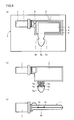
- guiding members 70 are arranged at two points in front of and at the rear of cavity to be fitted with 30, respectively, while guiding members 80 are arranged at two points on the right and left of external connection terminal 50 in a manner to adjoin opposing lateral surfaces of a tip end of external connection terminal 50, respectively.
- bottom mold 21 is provided with a pressing and supporting part 90 to support external connection terminal 50.
- Pressing and supporting part 90 presses a constricted portion 51, which is formed on each of the opposing lateral surfaces of external connection terminal 50, against a fixing member 91 provided at a predetermined position at bottom mold 21, thereby causing fixing member 91 to support external connection terminal 50.
- fixing members 91 are arranged at two points on the right and left on bottom mold 21 corresponding to the positions of right and left constricted portions 51, respectively.
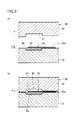
- a top mold 22 is arranged opposite bottom mold 21, as shown in Fig. 1 (b) .
- Bottom mold 21 and top mold 22 are arranged in a manner to enable opposing mold surfaces of bottom mold 21 and top mold 22 to be joined together (brought into contact) and separated from each other. It is noted that in a resin molding process, when a mold surface of a top mold and a mold surface of a bottom mold are joined together as shown in Fig. 1 (b) , it is called “mold clamping". On the other hand, when the mold surface of the top mold and the mold surface the bottom mold are separated from each other (see Fig. 2 ), it is called “mold opening".
- top mold 22 In a portion of the mold surface of top mold 22 opposite cavity to be fitted with 30 of bottom mold 21, a cavity to be fitted with 31 which is to be fitted with the upper half of resin molded article 10 is provided.
- a molding cavity 61 which is to be fitted with the upper halves of substrate 40 and external connection terminal 50 is provided.
- Pressing and supporting part 90 of external connection terminal 50 is provided so that when each component of the electrical circuit components is integrally resin encapsulated to mold a resin encapsulation molded body encapsulating an electrical circuit component, it is prevented that a resin lump (see resin lump 8a in Fig. 8 ) is formed through adhesion of part of an encapsulating melted resin material (flowable resin) to constricted portions 51 (see Fig. 6 ) formed on the opposing lateral surfaces of an external connection terminal 50a which will protrude from the resin encapsulation molded body.
- pressing and supporting part 90 includes fixing member 91 provided on bottom mold 21 and a pushing-out member 92 for pushing external connection terminal 50 out toward fixing member 91.
- fixing member 91 is provided at a position to be fitted to constricted portion 51 formed on each of the opposing lateral surfaces of external connection terminal 50.
- fixing members 91 are provided at predetermined positions at two points on the right and left on bottom mold 21 in a manner to correspond to the respective positions of constricted portions 51 at two points on the right and left of external connection terminal 50.
- Pushing-out member 92 is arranged at a portion of top mold 22 in the vicinity of the tip of external connection terminal 50 arranged on the mold surface of bottom mold 21.
- pushing-out members 92 are arranged at positions at two points on the right and left on the top mold. Further, pushing-out member 92 is arranged to be able to move vertically in top mold 22. In a state just before bottom mold 21 and top mold 22 are clamped together, pushing pushing-out member 92 down results in that a bottom surface portion of pushing-out member 92 adjoins the tip end of external connection terminal 50, and a tapered surface 92a formed on the bottom surface portion pushes the tip end of external connection terminal 50 out toward fixing member 91.
- cavity to be fitted with 30, 31 of mold for resin molding 20 is provided with a protrusion pin 23.
- Molding cavity 60, 61 is provided with a protrusion pin 24.
- the component fitted into cavity to be fitted with 30, 31 is held at a predetermined height (position) by causing a tip end portion of protrusion pin 23 to protrude into cavity to be fitted with 30, 31, while the component fitted into molding cavity 60, 61 is held at a predetermined height (position) by causing a tip end portion of protrusion pin 24 to protrude into molding cavity 60, 61.
- protrusion pins 23, 24 can serve as a supporting pin for each component.
- pushing-out member 92 of pressing and supporting parts 90 is shown as being arranged in a symmetrical pair (a multiple arrangement) on the top mold 22 at positions in front of right and left guiding members 80 provided at bottom mold 21.
- the pushing-out member one (single) pushing-out member may be provided, which is configured such that pushing the pushing-out member down results in that a bottom surface portion of the pushing-out member adjoins the tip end of the external connection terminal, and a tapered surface formed on the bottom surface portion pushes the tip end of external connection terminal out toward the fixing member.
- resin molded article (connector part) 10 is fitted into cavity to be fitted with 30 provided in the mold surface of bottom mold 21 of mold for resin molding 20, and glass epoxy substrate 40 and external connection terminal 50 are fitted into molding cavity 60 (the step of fitting a plurality of components).
- a plurality of components may be introduced between opened top mold 22 and bottom mold 21 automatically with any suitable carrying device or manually.
- the guiding member provided at the mold for resin molding guides the resin molded article to a predetermined position in the cavity to be fitted with and guides the substrate and the external connection terminal to the molding cavity (the step of assisting the fitting of a plurality of components). It is noted that this step may be performed simultaneously with the step of fitting a plurality of components.
- Tapered surface 71 of guiding member 70 provided at bottom mold 21 fits resin molded article 10 into cavity to be fitted with 30 and guides the lower half of resin molded article 10 to a predetermined position in cavity to be fitted with 30.
- Tapered surface 81 of guiding member 80 provided at bottom mold 21 fits external connection terminal 50 into molding cavity 60 and guides the lower half of external connection terminal 50 to a predetermined position in molding cavity 60.
- glass epoxy substrate 40 is one in which it is integrally connected to external connection terminal 50, then the above-described step of assisting the fitting of external connection terminal 50 causes glass epoxy substrate 40 to have its lower half fitted into molding cavity 60.
- glass epoxy substrate 40 and external connection terminal 50 are electrically connected but not made into one piece, then fitting resin molded article 10 into cavity to be fitted with 30 and fitting external connection terminal 50 into molding cavity 60 cause glass epoxy substrate 40 and external connection terminal 50 to sequentially have their respective lower halves fitted into molding cavity 60.
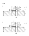
- External connection terminal 50 is then guided to a predetermined position, and two constricted portions 51, 51 of external connection terminal 50 are pressed against two fixing members 91, 91 so that external connection terminal 50 is supported by fixing members 91, 91 (the step of pressing and supporting an external connection terminal).
- two constricted portions 51, 51 of external connection terminal 50 are in a state of being fitted with two fixing members 91, 91 provided at mold for resin molding (bottom mold 21).
- top mold 22 is lowered to a position H at which the mold surface of top mold 22 and the mold surface of bottom mold 21 are just before being joined together, i.e. mold clamping.
- external connection terminal 50 is not under any mold clamping pressure applied by the top mold and the bottom mold.
- pushing pushing-out member 92 down in this state results in that the bottom surface portion of the pushing-out member adjoins the tip end of external connection terminal 50, and tapered surface 92a formed on the bottom surface portion pushes external connection terminal 50 out toward fixing member 91, as shown in Fig. 5 (a) .
- top mold 22 and the mold surface of bottom mold 21 are then joined together (the step of clamping molds).
- Glass epoxy substrate 40 and external connection terminal 50 are then encapsulated with a resin material, and the resin material encapsulating glass epoxy substrate 40 and the like are molded (the step of resin encapsulation molding a substrate and an external connection terminal).
- a thermosetting melted resin material (flowable resin) R is injected into molding cavity 60, 61 (see Fig. 1 (a) ) and fills molding cavity 60, 61.
- the resin material encapsulates glass epoxy substrate 40 and external connection terminal 50 which are fitted into the molding cavity, and the encapsulating resin material is molded.
- a resin encapsulation molded body (solidified resin) encapsulating glass epoxy substrate 40 and external connection terminal 50 is formed, and the resin encapsulation molded body and resin molded article (connector part) 10 are connected integrally together, so that a resin encapsulation molded article is formed.
- top mold 22 and the mold surface of bottom mold 21 are then separated from each other (the step of opening molds).
- the resin encapsulation molded article encapsulating an electrical circuit component is then removed from between top mold 22 and bottom mold 21 (the step of removing a product).
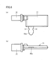
- resin molded article (connector part) 10 and a resin encapsulation molded body 77 encapsulating the glass epoxy substrate and the external connection terminal are integrally connected together, so that they are made into one piece.
- No resin lump or resin flash is formed on two constricted portions 51, 51 of and upper and lower surfaces of terminal 50a which protrudes from resin encapsulating molded body 77.
- the resin encapsulation molding apparatus according to the second embodiment has a structure which can further ensure that a resin flash is prevented from being formed on a surface of terminal 50a protruding from resin encapsulation molded body 77. It is noted that to avoid redundancy in the description, same members as those of the above-described resin encapsulation molding apparatus have the same reference characters allotted in Fig. 7 .
- the tip end of external connection terminal 50 which is not fitted into molding cavity 61, 60 of top mold 22 and bottom mold 21, will be sandwiched between the mold surface of the top mold and the mold surface of the bottom mold, under a mold clamping pressure.
- the tip end of external connection terminal serves as terminal 50a for external connection which protrudes from resin encapsulating molded body 77 (see Fig. 6 ).
- connection terminal 50 when the tip end of connection terminal 50 is under an appropriate mold clamping pressure applied by the top mold and the bottom mold, it can be prevented that a resin flash is formed through adhesion of part of a melted resin material (flowable resin) to a surface of terminal 50a.
- external connection terminal 50 varies in thickness. For this reason, for example, when the external connection terminal has a thickness less than a predetermined thickness, in clamping the top mold and the bottom mold together, a gap may develop between the tip end of the external connection terminal and the mold surface of the top mold or the mold surface of the bottom mold. If so, this gap may cause a resin flash to be formed through adhesion of part of the molten resin material to a surface of terminal 50a.
- a resin flash adhesion preventing part having a pressing member is provided so that in clamping top mold 22 and bottom mold 21 together, no gap develops between a surface of terminal 50a protruding from resin encapsulation molded body 77 and the mold surface of top mold 22 or the mold surface of bottom mold 21.
- the resin flash adhesion preventing part 93 includes the pressing member 93a fitted into top mold 22 in a vertically movable manner and an elastic member 93b. Pressing member 93a is pushed out downward because of the elasticity of elastic member 93b. In clamping top mold 22 and bottom mold 21 together, a pressing surface 93c provided on the bottom end surface of pressing member 93a comes into contact with a surface (upper surface) of terminal 50a arranged on bottom mold 21, by means of elastic force.
- Fig. 7 shows the resin encapsulation molding apparatus in which resin flash adhesion preventing part 93 is provided only at top mold 22, a resin flash adhesion preventing part having the same functions may also be provided at bottom mold 21.
- pressing surfaces of the pressing members come into contact with the front surface (upper surface) and the back surface (lower surface) of terminal 50a, respectively, by means of elastic force.
- pressing surface 93c of pressing member 93a comes into contact with a surface of terminal 50a by means of elastic force just before top mold 22 and bottom mold 21 are clamped together (the step of preventing adhesion of a resin flash).
- thermosetting resin material is used as a resin material in each embodiment above
- thermoplastic resin material may be employed.
- resin materials in various shapes such as a granular resin material (granular resin), a liquid resin material (liquid resin), a powdered resin material having a prescribed particle size distribution (powdered resin), a powdery resin material (powdery resin), a pasty resin material (pasty resin), a tablet resin material (tablet resin), or the like can be employed.
- epoxy resin epoxy resin
- silicon-based resin material silicon resin
- a technique for injecting flowable resin R into molding cavity 60, 61 and filling the molding cavity a known method of injecting and filling can be used.
- a transfer molding, an injection molding, or the like can be used.
- a resin tablet (epoxy-based resin material) supplied into a pot is heated to melt.
- the melted resin material flowable resin
- the melted resin material is injected via a resin path (a cull part, a runner, a gate) into molding cavity 60, 61 and fills the molding cavity.
- a mold for resin molding (a top mold, a bottom mold) can be opened, thereby providing a resin encapsulation molded article encapsulating an electrical circuit component.
Landscapes
- Engineering & Computer Science (AREA)
- Manufacturing & Machinery (AREA)
- Mechanical Engineering (AREA)
- Encapsulation Of And Coatings For Semiconductor Or Solid State Devices (AREA)
- Injection Moulding Of Plastics Or The Like (AREA)
- Moulds For Moulding Plastics Or The Like (AREA)
- Non-Metallic Protective Coatings For Printed Circuits (AREA)
Applications Claiming Priority (1)
| Application Number | Priority Date | Filing Date | Title |
|---|---|---|---|
| JP2010245906A JP5385886B2 (ja) | 2010-11-02 | 2010-11-02 | 電気回路部品の樹脂封止成形方法及び装置 |
Publications (2)
| Publication Number | Publication Date |
|---|---|
| EP2447986A1 true EP2447986A1 (de) | 2012-05-02 |
| EP2447986B1 EP2447986B1 (de) | 2014-06-04 |
Family
ID=45001640
Family Applications (1)
| Application Number | Title | Priority Date | Filing Date |
|---|---|---|---|
| EP11186409.6A Active EP2447986B1 (de) | 2010-11-02 | 2011-10-24 | Harzformverfahren zur Verkapselung und Vorrichtung für elektrische Schaltkomponente |
Country Status (4)
| Country | Link |
|---|---|
| EP (1) | EP2447986B1 (de) |
| JP (1) | JP5385886B2 (de) |
| KR (1) | KR101311027B1 (de) |
| CN (1) | CN102463653B (de) |
Cited By (1)
| Publication number | Priority date | Publication date | Assignee | Title |
|---|---|---|---|---|
| DE102019121229A1 (de) * | 2019-08-06 | 2021-02-11 | Infineon Technologies Ag | Elektronische Vorrichtungen mit elektrisch isolierten Lastelektroden |
Families Citing this family (6)
| Publication number | Priority date | Publication date | Assignee | Title |
|---|---|---|---|---|
| WO2013136926A1 (ja) * | 2012-03-16 | 2013-09-19 | 株式会社村田製作所 | 封止用樹脂シートの製造装置および封止用樹脂シートの製造方法 |
| CN102738020A (zh) * | 2012-06-26 | 2012-10-17 | 铜陵三佳山田科技有限公司 | 一种防止型芯孔处水平溢料的集成电路塑料封装模具 |
| JP6804410B2 (ja) * | 2017-08-09 | 2020-12-23 | Towa株式会社 | 搬送機構、樹脂成形装置、成形対象物の成形型への受け渡し方法、及び樹脂成形品の製造方法 |
| US11145966B2 (en) * | 2019-08-28 | 2021-10-12 | Pctel, Inc. | Over-molded thin film antenna device |
| CN114889039A (zh) * | 2022-04-19 | 2022-08-12 | 微智医疗器械有限公司 | 视网膜植入体柔性电极及其包胶模具、包胶方法 |
| CN117207442A (zh) * | 2023-11-09 | 2023-12-12 | 成都宝利根创科电子有限公司 | 一种端子模内成型方法 |
Citations (6)
| Publication number | Priority date | Publication date | Assignee | Title |
|---|---|---|---|---|
| EP0257681A2 (de) * | 1986-08-27 | 1988-03-02 | STMicroelectronics S.r.l. | Verfahren zur Herstellung von in Kunststoff eingeschmolzenen Halbleiterbauelementen und damit hergestellte Bauelemente |
| US5384286A (en) * | 1991-08-16 | 1995-01-24 | Mitsubishi Denki Kabushiki Kaisha | Process for encapsulating a semiconductor chip, leadframe and heatsink |
| JP2003037241A (ja) | 2001-07-24 | 2003-02-07 | Hitachi Ltd | 電気回路基板パッケージ品および電気回路基板パッケージ品の製造方法 |
| US20030180985A1 (en) * | 2002-03-20 | 2003-09-25 | Mitsubishi Denki Kabushiki Kaisha | Method for manufacturing a semiconductor device and a resin sealing device therefor |
| US20040166605A1 (en) * | 2002-10-10 | 2004-08-26 | Bunshi Kuratomi | Fabrication method of semiconductor integrated circuit device |
| WO2010038660A1 (ja) * | 2008-09-30 | 2010-04-08 | Towa株式会社 | 電子部品の圧縮樹脂封止成形方法及びそのための装置 |
Family Cites Families (8)
| Publication number | Priority date | Publication date | Assignee | Title |
|---|---|---|---|---|
| JPH0831489B2 (ja) * | 1987-07-20 | 1996-03-27 | サンケン電気株式会社 | 樹脂封止型電気部品の製造方法 |
| JP3397741B2 (ja) * | 2000-03-07 | 2003-04-21 | Towa株式会社 | 基板の位置決め機構及び位置決め方法 |
| JP4153862B2 (ja) * | 2003-10-24 | 2008-09-24 | 第一精工株式会社 | 半導体樹脂封止用金型 |
| JP4084844B2 (ja) * | 2005-09-27 | 2008-04-30 | Towa株式会社 | 電子部品の樹脂封止成形方法及び装置 |
| JP2007095804A (ja) * | 2005-09-27 | 2007-04-12 | Towa Corp | 電子部品の樹脂封止成形方法及び装置 |
| JP2007281364A (ja) * | 2006-04-11 | 2007-10-25 | Towa Corp | 電子部品の樹脂封止成形方法及び装置 |
| JP2009124012A (ja) * | 2007-11-16 | 2009-06-04 | Towa Corp | 電子部品の圧縮成形方法及び金型 |
| JP5056717B2 (ja) * | 2008-10-16 | 2012-10-24 | 株式会社デンソー | モールドパッケージの製造方法 |
-
2010
- 2010-11-02 JP JP2010245906A patent/JP5385886B2/ja active Active
-
2011
- 2011-10-24 EP EP11186409.6A patent/EP2447986B1/de active Active
- 2011-10-26 KR KR1020110109710A patent/KR101311027B1/ko active Active
- 2011-11-02 CN CN201110344139.4A patent/CN102463653B/zh active Active
Patent Citations (6)
| Publication number | Priority date | Publication date | Assignee | Title |
|---|---|---|---|---|
| EP0257681A2 (de) * | 1986-08-27 | 1988-03-02 | STMicroelectronics S.r.l. | Verfahren zur Herstellung von in Kunststoff eingeschmolzenen Halbleiterbauelementen und damit hergestellte Bauelemente |
| US5384286A (en) * | 1991-08-16 | 1995-01-24 | Mitsubishi Denki Kabushiki Kaisha | Process for encapsulating a semiconductor chip, leadframe and heatsink |
| JP2003037241A (ja) | 2001-07-24 | 2003-02-07 | Hitachi Ltd | 電気回路基板パッケージ品および電気回路基板パッケージ品の製造方法 |
| US20030180985A1 (en) * | 2002-03-20 | 2003-09-25 | Mitsubishi Denki Kabushiki Kaisha | Method for manufacturing a semiconductor device and a resin sealing device therefor |
| US20040166605A1 (en) * | 2002-10-10 | 2004-08-26 | Bunshi Kuratomi | Fabrication method of semiconductor integrated circuit device |
| WO2010038660A1 (ja) * | 2008-09-30 | 2010-04-08 | Towa株式会社 | 電子部品の圧縮樹脂封止成形方法及びそのための装置 |
Cited By (3)
| Publication number | Priority date | Publication date | Assignee | Title |
|---|---|---|---|---|
| DE102019121229A1 (de) * | 2019-08-06 | 2021-02-11 | Infineon Technologies Ag | Elektronische Vorrichtungen mit elektrisch isolierten Lastelektroden |
| US11646258B2 (en) | 2019-08-06 | 2023-05-09 | Infineon Technologies Ag | Electronic devices including electrically insulated load electrodes |
| DE102019121229B4 (de) * | 2019-08-06 | 2025-08-14 | Infineon Technologies Ag | Elektronische Vorrichtungen mit elektrisch isolierten Lastelektroden und zugehörige Herstellungsverfahren |
Also Published As
| Publication number | Publication date |
|---|---|
| JP2012099628A (ja) | 2012-05-24 |
| KR101311027B1 (ko) | 2013-09-24 |
| CN102463653A (zh) | 2012-05-23 |
| CN102463653B (zh) | 2014-09-17 |
| EP2447986B1 (de) | 2014-06-04 |
| KR20120046684A (ko) | 2012-05-10 |
| JP5385886B2 (ja) | 2014-01-08 |
Similar Documents
| Publication | Publication Date | Title |
|---|---|---|
| EP2447986A1 (de) | Harzformverfahren zur Verkapselung und Vorrichtung für elektrische Schaltkomponente | |
| US8202457B2 (en) | Method and apparatus for producing battery pack | |
| KR101006621B1 (ko) | 전자 회로 장치 및 이의 제조 방법 | |
| US12255080B2 (en) | Semiconductor manufacturing apparatus and method of manufacturing semiconductor device using the same, and semiconductor device | |
| CN105280506B (zh) | 电子部件的树脂封装方法及树脂封装装置 | |
| US8300419B2 (en) | Electronic circuit device and method of making the same | |
| CN108028235B (zh) | 树脂封装装置以及树脂封装方法 | |
| TWI778332B (zh) | 樹脂成形裝置以及樹脂成形品的製造方法 | |
| US8122592B2 (en) | Method for producing a low-current switch module comprising electrical components | |
| KR960700875A (ko) | 반도체 장치의 수지봉지 방법 | |
| CN109383047B (zh) | 树脂成型装置以及树脂成型品的制造方法 | |
| JPH0521492A (ja) | 電気・電子部品の樹脂封止成形方法及びそれに用いる金型 | |
| KR102259426B1 (ko) | 압축 성형 장치, 압축 성형 방법 및 압축 성형품의 제조 방법 | |
| JPH0976282A (ja) | 電気・電子部品の樹脂封止成形方法及びそれに用いる金型 | |
| JPH03202327A (ja) | 樹脂成形用金型面のクリーニング方法とこの方法に用いられるクリーニング用シート部材及び連続自動樹脂成形方法 | |
| US6682952B2 (en) | Method of forming the resin sealed semiconductor device using the lead frame | |
| CN102157822B (zh) | 包括热熔元件的电气部件及其制造方法和工具 | |
| CN101017788A (zh) | 半导体装置的制造方法及半导体装置的制造装置 | |
| JP6861507B2 (ja) | 圧縮成形装置、圧縮成形方法、及び圧縮成形品の製造方法 | |
| JP2004311855A (ja) | 電子部品の樹脂封止成形用金型 | |
| TW421868B (en) | Device and method for encapsulating electronic component mounted on a carrier | |
| JP3795684B2 (ja) | 電子部品の樹脂封止成形方法 | |
| JP5723800B2 (ja) | 半導体チップの圧縮樹脂封止成形方法及び装置 | |
| JP2772489B2 (ja) | 電子部品の樹脂封止成形装置及びエジェクターピンの押込用治具 | |
| GB2054447A (en) | Encapsulating semiconductor devices by injection moulding |
Legal Events
| Date | Code | Title | Description |
|---|---|---|---|
| PUAI | Public reference made under article 153(3) epc to a published international application that has entered the european phase |
Free format text: ORIGINAL CODE: 0009012 |
|
| AK | Designated contracting states |
Kind code of ref document: A1 Designated state(s): AL AT BE BG CH CY CZ DE DK EE ES FI FR GB GR HR HU IE IS IT LI LT LU LV MC MK MT NL NO PL PT RO RS SE SI SK SM TR |
|
| AX | Request for extension of the european patent |
Extension state: BA ME |
|
| 17P | Request for examination filed |
Effective date: 20120613 |
|
| RIC1 | Information provided on ipc code assigned before grant |
Ipc: H01L 23/31 20060101ALI20130715BHEP Ipc: B29C 45/14 20060101ALI20130715BHEP Ipc: H01L 21/56 20060101AFI20130715BHEP Ipc: H01L 21/67 20060101ALI20130715BHEP |
|
| 17Q | First examination report despatched |
Effective date: 20130808 |
|
| GRAP | Despatch of communication of intention to grant a patent |
Free format text: ORIGINAL CODE: EPIDOSNIGR1 |
|
| INTG | Intention to grant announced |
Effective date: 20140116 |
|
| GRAS | Grant fee paid |
Free format text: ORIGINAL CODE: EPIDOSNIGR3 |
|
| GRAA | (expected) grant |
Free format text: ORIGINAL CODE: 0009210 |
|
| AK | Designated contracting states |
Kind code of ref document: B1 Designated state(s): AL AT BE BG CH CY CZ DE DK EE ES FI FR GB GR HR HU IE IS IT LI LT LU LV MC MK MT NL NO PL PT RO RS SE SI SK SM TR |
|
| REG | Reference to a national code |
Ref country code: GB Ref legal event code: FG4D |
|
| REG | Reference to a national code |
Ref country code: CH Ref legal event code: EP |
|
| REG | Reference to a national code |
Ref country code: AT Ref legal event code: REF Ref document number: 671508 Country of ref document: AT Kind code of ref document: T Effective date: 20140615 |
|
| REG | Reference to a national code |
Ref country code: IE Ref legal event code: FG4D |
|
| REG | Reference to a national code |
Ref country code: DE Ref legal event code: R096 Ref document number: 602011007384 Country of ref document: DE Effective date: 20140717 |
|
| REG | Reference to a national code |
Ref country code: AT Ref legal event code: MK05 Ref document number: 671508 Country of ref document: AT Kind code of ref document: T Effective date: 20140604 |
|
| REG | Reference to a national code |
Ref country code: NL Ref legal event code: VDEP Effective date: 20140604 |
|
| PG25 | Lapsed in a contracting state [announced via postgrant information from national office to epo] |
Ref country code: LT Free format text: LAPSE BECAUSE OF FAILURE TO SUBMIT A TRANSLATION OF THE DESCRIPTION OR TO PAY THE FEE WITHIN THE PRESCRIBED TIME-LIMIT Effective date: 20140604 Ref country code: FI Free format text: LAPSE BECAUSE OF FAILURE TO SUBMIT A TRANSLATION OF THE DESCRIPTION OR TO PAY THE FEE WITHIN THE PRESCRIBED TIME-LIMIT Effective date: 20140604 Ref country code: CY Free format text: LAPSE BECAUSE OF FAILURE TO SUBMIT A TRANSLATION OF THE DESCRIPTION OR TO PAY THE FEE WITHIN THE PRESCRIBED TIME-LIMIT Effective date: 20140604 Ref country code: GR Free format text: LAPSE BECAUSE OF FAILURE TO SUBMIT A TRANSLATION OF THE DESCRIPTION OR TO PAY THE FEE WITHIN THE PRESCRIBED TIME-LIMIT Effective date: 20140905 Ref country code: NO Free format text: LAPSE BECAUSE OF FAILURE TO SUBMIT A TRANSLATION OF THE DESCRIPTION OR TO PAY THE FEE WITHIN THE PRESCRIBED TIME-LIMIT Effective date: 20140904 |
|
| REG | Reference to a national code |
Ref country code: LT Ref legal event code: MG4D |
|
| PG25 | Lapsed in a contracting state [announced via postgrant information from national office to epo] |
Ref country code: SE Free format text: LAPSE BECAUSE OF FAILURE TO SUBMIT A TRANSLATION OF THE DESCRIPTION OR TO PAY THE FEE WITHIN THE PRESCRIBED TIME-LIMIT Effective date: 20140604 Ref country code: AT Free format text: LAPSE BECAUSE OF FAILURE TO SUBMIT A TRANSLATION OF THE DESCRIPTION OR TO PAY THE FEE WITHIN THE PRESCRIBED TIME-LIMIT Effective date: 20140604 Ref country code: LV Free format text: LAPSE BECAUSE OF FAILURE TO SUBMIT A TRANSLATION OF THE DESCRIPTION OR TO PAY THE FEE WITHIN THE PRESCRIBED TIME-LIMIT Effective date: 20140604 Ref country code: RS Free format text: LAPSE BECAUSE OF FAILURE TO SUBMIT A TRANSLATION OF THE DESCRIPTION OR TO PAY THE FEE WITHIN THE PRESCRIBED TIME-LIMIT Effective date: 20140604 Ref country code: HR Free format text: LAPSE BECAUSE OF FAILURE TO SUBMIT A TRANSLATION OF THE DESCRIPTION OR TO PAY THE FEE WITHIN THE PRESCRIBED TIME-LIMIT Effective date: 20140604 |
|
| REG | Reference to a national code |
Ref country code: HU Ref legal event code: AG4A Ref document number: E021515 Country of ref document: HU |
|
| PG25 | Lapsed in a contracting state [announced via postgrant information from national office to epo] |
Ref country code: CZ Free format text: LAPSE BECAUSE OF FAILURE TO SUBMIT A TRANSLATION OF THE DESCRIPTION OR TO PAY THE FEE WITHIN THE PRESCRIBED TIME-LIMIT Effective date: 20140604 Ref country code: ES Free format text: LAPSE BECAUSE OF FAILURE TO SUBMIT A TRANSLATION OF THE DESCRIPTION OR TO PAY THE FEE WITHIN THE PRESCRIBED TIME-LIMIT Effective date: 20140604 Ref country code: PT Free format text: LAPSE BECAUSE OF FAILURE TO SUBMIT A TRANSLATION OF THE DESCRIPTION OR TO PAY THE FEE WITHIN THE PRESCRIBED TIME-LIMIT Effective date: 20141006 Ref country code: RO Free format text: LAPSE BECAUSE OF FAILURE TO SUBMIT A TRANSLATION OF THE DESCRIPTION OR TO PAY THE FEE WITHIN THE PRESCRIBED TIME-LIMIT Effective date: 20140604 Ref country code: SK Free format text: LAPSE BECAUSE OF FAILURE TO SUBMIT A TRANSLATION OF THE DESCRIPTION OR TO PAY THE FEE WITHIN THE PRESCRIBED TIME-LIMIT Effective date: 20140604 Ref country code: EE Free format text: LAPSE BECAUSE OF FAILURE TO SUBMIT A TRANSLATION OF THE DESCRIPTION OR TO PAY THE FEE WITHIN THE PRESCRIBED TIME-LIMIT Effective date: 20140604 |
|
| PG25 | Lapsed in a contracting state [announced via postgrant information from national office to epo] |
Ref country code: NL Free format text: LAPSE BECAUSE OF FAILURE TO SUBMIT A TRANSLATION OF THE DESCRIPTION OR TO PAY THE FEE WITHIN THE PRESCRIBED TIME-LIMIT Effective date: 20140604 Ref country code: IS Free format text: LAPSE BECAUSE OF FAILURE TO SUBMIT A TRANSLATION OF THE DESCRIPTION OR TO PAY THE FEE WITHIN THE PRESCRIBED TIME-LIMIT Effective date: 20141004 Ref country code: PL Free format text: LAPSE BECAUSE OF FAILURE TO SUBMIT A TRANSLATION OF THE DESCRIPTION OR TO PAY THE FEE WITHIN THE PRESCRIBED TIME-LIMIT Effective date: 20140604 |
|
| REG | Reference to a national code |
Ref country code: DE Ref legal event code: R097 Ref document number: 602011007384 Country of ref document: DE |
|
| PLBE | No opposition filed within time limit |
Free format text: ORIGINAL CODE: 0009261 |
|
| STAA | Information on the status of an ep patent application or granted ep patent |
Free format text: STATUS: NO OPPOSITION FILED WITHIN TIME LIMIT |
|
| PG25 | Lapsed in a contracting state [announced via postgrant information from national office to epo] |
Ref country code: IT Free format text: LAPSE BECAUSE OF FAILURE TO SUBMIT A TRANSLATION OF THE DESCRIPTION OR TO PAY THE FEE WITHIN THE PRESCRIBED TIME-LIMIT Effective date: 20140604 Ref country code: DK Free format text: LAPSE BECAUSE OF FAILURE TO SUBMIT A TRANSLATION OF THE DESCRIPTION OR TO PAY THE FEE WITHIN THE PRESCRIBED TIME-LIMIT Effective date: 20140604 |
|
| 26N | No opposition filed |
Effective date: 20150305 |
|
| PG25 | Lapsed in a contracting state [announced via postgrant information from national office to epo] |
Ref country code: LU Free format text: LAPSE BECAUSE OF FAILURE TO SUBMIT A TRANSLATION OF THE DESCRIPTION OR TO PAY THE FEE WITHIN THE PRESCRIBED TIME-LIMIT Effective date: 20141024 Ref country code: MC Free format text: LAPSE BECAUSE OF FAILURE TO SUBMIT A TRANSLATION OF THE DESCRIPTION OR TO PAY THE FEE WITHIN THE PRESCRIBED TIME-LIMIT Effective date: 20140604 |
|
| REG | Reference to a national code |
Ref country code: CH Ref legal event code: PL |
|
| REG | Reference to a national code |
Ref country code: DE Ref legal event code: R097 Ref document number: 602011007384 Country of ref document: DE Effective date: 20150305 |
|
| REG | Reference to a national code |
Ref country code: IE Ref legal event code: MM4A |
|
| PG25 | Lapsed in a contracting state [announced via postgrant information from national office to epo] |
Ref country code: LI Free format text: LAPSE BECAUSE OF NON-PAYMENT OF DUE FEES Effective date: 20141031 Ref country code: SI Free format text: LAPSE BECAUSE OF FAILURE TO SUBMIT A TRANSLATION OF THE DESCRIPTION OR TO PAY THE FEE WITHIN THE PRESCRIBED TIME-LIMIT Effective date: 20140604 Ref country code: CH Free format text: LAPSE BECAUSE OF NON-PAYMENT OF DUE FEES Effective date: 20141031 |
|
| REG | Reference to a national code |
Ref country code: FR Ref legal event code: ST Effective date: 20150630 |
|
| PG25 | Lapsed in a contracting state [announced via postgrant information from national office to epo] |
Ref country code: FR Free format text: LAPSE BECAUSE OF NON-PAYMENT OF DUE FEES Effective date: 20141031 |
|
| PG25 | Lapsed in a contracting state [announced via postgrant information from national office to epo] |
Ref country code: IE Free format text: LAPSE BECAUSE OF NON-PAYMENT OF DUE FEES Effective date: 20141024 |
|
| PG25 | Lapsed in a contracting state [announced via postgrant information from national office to epo] |
Ref country code: SM Free format text: LAPSE BECAUSE OF FAILURE TO SUBMIT A TRANSLATION OF THE DESCRIPTION OR TO PAY THE FEE WITHIN THE PRESCRIBED TIME-LIMIT Effective date: 20140604 |
|
| GBPC | Gb: european patent ceased through non-payment of renewal fee |
Effective date: 20151024 |
|
| PG25 | Lapsed in a contracting state [announced via postgrant information from national office to epo] |
Ref country code: BG Free format text: LAPSE BECAUSE OF FAILURE TO SUBMIT A TRANSLATION OF THE DESCRIPTION OR TO PAY THE FEE WITHIN THE PRESCRIBED TIME-LIMIT Effective date: 20140604 |
|
| PG25 | Lapsed in a contracting state [announced via postgrant information from national office to epo] |
Ref country code: GB Free format text: LAPSE BECAUSE OF NON-PAYMENT OF DUE FEES Effective date: 20151024 Ref country code: MT Free format text: LAPSE BECAUSE OF FAILURE TO SUBMIT A TRANSLATION OF THE DESCRIPTION OR TO PAY THE FEE WITHIN THE PRESCRIBED TIME-LIMIT Effective date: 20140604 Ref country code: BE Free format text: LAPSE BECAUSE OF FAILURE TO SUBMIT A TRANSLATION OF THE DESCRIPTION OR TO PAY THE FEE WITHIN THE PRESCRIBED TIME-LIMIT Effective date: 20140604 Ref country code: TR Free format text: LAPSE BECAUSE OF FAILURE TO SUBMIT A TRANSLATION OF THE DESCRIPTION OR TO PAY THE FEE WITHIN THE PRESCRIBED TIME-LIMIT Effective date: 20140604 |
|
| PG25 | Lapsed in a contracting state [announced via postgrant information from national office to epo] |
Ref country code: MK Free format text: LAPSE BECAUSE OF FAILURE TO SUBMIT A TRANSLATION OF THE DESCRIPTION OR TO PAY THE FEE WITHIN THE PRESCRIBED TIME-LIMIT Effective date: 20140604 |
|
| PG25 | Lapsed in a contracting state [announced via postgrant information from national office to epo] |
Ref country code: AL Free format text: LAPSE BECAUSE OF FAILURE TO SUBMIT A TRANSLATION OF THE DESCRIPTION OR TO PAY THE FEE WITHIN THE PRESCRIBED TIME-LIMIT Effective date: 20140604 |
|
| P01 | Opt-out of the competence of the unified patent court (upc) registered |
Effective date: 20230525 |
|
| PGFP | Annual fee paid to national office [announced via postgrant information from national office to epo] |
Ref country code: HU Payment date: 20251027 Year of fee payment: 15 |
|
| REG | Reference to a national code |
Ref country code: DE Ref legal event code: R079 Ref document number: 602011007384 Country of ref document: DE Free format text: PREVIOUS MAIN CLASS: H01L0021560000 Ipc: H10W0074010000 |
|
| PGFP | Annual fee paid to national office [announced via postgrant information from national office to epo] |
Ref country code: DE Payment date: 20251021 Year of fee payment: 15 |