EP2451068A2 - Motorantriebsvorrichtung - Google Patents
Motorantriebsvorrichtung Download PDFInfo
- Publication number
- EP2451068A2 EP2451068A2 EP11158797A EP11158797A EP2451068A2 EP 2451068 A2 EP2451068 A2 EP 2451068A2 EP 11158797 A EP11158797 A EP 11158797A EP 11158797 A EP11158797 A EP 11158797A EP 2451068 A2 EP2451068 A2 EP 2451068A2
- Authority
- EP
- European Patent Office
- Prior art keywords
- motor drive
- switching transistors
- drive circuit
- transistor
- gate
- Prior art date
- Legal status (The legal status is an assumption and is not a legal conclusion. Google has not performed a legal analysis and makes no representation as to the accuracy of the status listed.)
- Granted
Links
Images


Classifications
-
- H—ELECTRICITY
- H02—GENERATION; CONVERSION OR DISTRIBUTION OF ELECTRIC POWER
- H02M—APPARATUS FOR CONVERSION BETWEEN AC AND AC, BETWEEN AC AND DC, OR BETWEEN DC AND DC, AND FOR USE WITH MAINS OR SIMILAR POWER SUPPLY SYSTEMS; CONVERSION OF DC OR AC INPUT POWER INTO SURGE OUTPUT POWER; CONTROL OR REGULATION THEREOF
- H02M7/00—Conversion of AC power input into DC power output; Conversion of DC power input into AC power output
- H02M7/42—Conversion of DC power input into AC power output without possibility of reversal
- H02M7/44—Conversion of DC power input into AC power output without possibility of reversal by static converters
- H02M7/48—Conversion of DC power input into AC power output without possibility of reversal by static converters using discharge tubes with control electrode or semiconductor devices with control electrode
- H02M7/53—Conversion of DC power input into AC power output without possibility of reversal by static converters using discharge tubes with control electrode or semiconductor devices with control electrode using devices of a triode or transistor type requiring continuous application of a control signal
- H02M7/537—Conversion of DC power input into AC power output without possibility of reversal by static converters using discharge tubes with control electrode or semiconductor devices with control electrode using devices of a triode or transistor type requiring continuous application of a control signal using semiconductor devices only, e.g. single switched pulse inverters
- H02M7/5387—Conversion of DC power input into AC power output without possibility of reversal by static converters using discharge tubes with control electrode or semiconductor devices with control electrode using devices of a triode or transistor type requiring continuous application of a control signal using semiconductor devices only, e.g. single switched pulse inverters in a bridge configuration
-
- H—ELECTRICITY
- H02—GENERATION; CONVERSION OR DISTRIBUTION OF ELECTRIC POWER
- H02P—CONTROL OR REGULATION OF ELECTRIC MOTORS, ELECTRIC GENERATORS OR DYNAMO-ELECTRIC CONVERTERS; CONTROLLING TRANSFORMERS, REACTORS OR CHOKE COILS
- H02P27/00—Arrangements or methods for the control of AC motors characterised by the kind of supply voltage
- H02P27/04—Arrangements or methods for the control of AC motors characterised by the kind of supply voltage using variable-frequency supply voltage, e.g. inverter or converter supply voltage
- H02P27/06—Arrangements or methods for the control of AC motors characterised by the kind of supply voltage using variable-frequency supply voltage, e.g. inverter or converter supply voltage using DC to AC converters or inverters
-
- H—ELECTRICITY
- H03—ELECTRONIC CIRCUITRY
- H03K—PULSE TECHNIQUE
- H03K17/00—Electronic switching or gating, i.e. not by contact-making and –breaking
- H03K17/08—Modifications for protecting switching circuit against overcurrent or overvoltage
- H03K17/081—Modifications for protecting switching circuit against overcurrent or overvoltage without feedback from the output circuit to the control circuit
- H03K17/0812—Modifications for protecting switching circuit against overcurrent or overvoltage without feedback from the output circuit to the control circuit by measures taken in the control circuit
- H03K17/08122—Modifications for protecting switching circuit against overcurrent or overvoltage without feedback from the output circuit to the control circuit by measures taken in the control circuit in field-effect transistor switches
Definitions
- the present invention relates to a motor drive device that drives a motor in a controlled manner by a motor drive circuit configured with a bridge connection of switching transistors.
- resisters each are disposed and connected between the gate and source of switching transistors, such as FETs (field effect transistors) or bipolar transistors (between the base and emitter in the case of bipolar transistors), used for a motor drive circuit, whereby when its drive signal path comes into a high-impedance or open state, gate charge is discharged and gate voltage is decreased to lower than a threshold voltage at which the transistors turn off.
- FETs field effect transistors
- bipolar transistors between the base and emitter in the case of bipolar transistors
- Patent Document 1 Japanese Patent No. 2819878 ( FIG. 1 and FIG. 4 )
- the present invention has been made to solve the problems described above, which aims at providing a motor drive device in which even when an open-circuit failure occurs in a drive signal path inside the motor drive device, the device does not fall into a dangerous situation such as switching transistors turning on, causing a short-circuit current and transistor breakdown, so that the transistors of the motor drive circuit can be brought into a safe off-state.
- a motor drive device comprises: a motor drive circuit that includes switching transistors connected in a bridge configuration and to which are connected a motor drive power supply between the input terminals thereof and a motor between the output terminals thereof; and a transistor drive circuit that supplies a drive signal to the switching transistors of the motor drive circuit and takes on/off control of the switching transistors; wherein resisters are connected between the gate and source (or the base and emitter) of each of the switching transistors of the motor drive circuit so as to turn off the switching transistors when an open-circuit failure occurs in a drive signal path from the motor drive circuit to the switching transistors, and the resisters are disposed inside the respective switching transistors.
- a motor drive device comprises: a motor drive circuit that includes switching transistors connected in a bridge configuration and to which are connected a motor drive power supply between the input terminals thereof and a motor between the output terminals thereof; and a transistor drive circuit that supplies a drive signal to the transistors of the motor drive circuit and takes on/off control of the switching transistors; wherein capacitors are connected between the gate and source (or the base and emitter) of each of the switching transistors of the motor drive circuit so as to turn off the switching transistors when an open-circuit failure occurs in a drive signal path from the motor drive circuit to the switching transistors, and the capacitors are disposed inside the respective switching transistors.
- a motor drive device can be provided in which even when an open-circuit failure occurs in a drive signal path in the motor drive device, the device does not fall into a dangerous situation such as the switching transistors turning on, causing a short-circuit current and transistor breakdown, so that the transistors of the motor drive circuit can be safely brought into the off-state without fail.
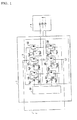
- FIG. 1 is a circuit, configuration diagram of a motor drive device according to Embodiment 1 of the present invention.
- a motor drive circuit 3 includes semiconductor switching transistors (hereinafter simply referred to as transistors) Q1 to Q6, such as FETs (field effect transistors) or bipolar transistors, connected in a bridge configuration, and to which are connected a motor drive power supply 2 between the input terminals thereof and a motor 4 between the output terminals thereof.
- transistors semiconductor switching transistors (hereinafter simply referred to as transistors) Q1 to Q6, such as FETs (field effect transistors) or bipolar transistors, connected in a bridge configuration, and to which are connected a motor drive power supply 2 between the input terminals thereof and a motor 4 between the output terminals thereof.
- a transistor drive circuit 50 sends a drive signal to the motor drive circuit 3 and takes on/off control of each of the transistors Q1 to Q6, thereby converting power supplied from the power supply 2 so as to drive the motor 4.
- the drive signal output from the transistor drive circuit 50 is input to the gate (or base) of the transistors Q1 to Q6 via a wiring pattern and a bus bar of the substrate configured inside the motor drive device 1, gate resisters Rg1 to Rg6 provided for controlling switching speed of the transistors and preventing oscillation thereof, junctions of the substrate with the bus bar and so forth.
- the resisters between gate and source Rgs1 to Rgs6 are disposed and connected between the gate and source inside the respective transistors Q1 to Q6 in order to bring the transistors into an off-state without fail, when the transistor drive circuit 50 outputs an off-signal or even when an open-circuit or high-impedance failure occurs in the drive signal path.
- the resisters between gate and source Rgs1 to Rgs6 are disposed and connected inside the respective transistors Q1 to Q6; therefore, even when an open-circuit or high-impedance failure occurs in the drive signal path in which the drive signal from the transistor drive circuit 50 is input to the transistors Q1 to Q6, the resisters between gate and source Rgs1 to Rgs6 remain connected with the transistors Q1 to Q6 so as to properly fulfill their function, whereby the transistor connected to the signal path in which the failure occurs can be brought into the off-state without fail.
- FIG. 2 is a connection diagram for explaining the internal configuration of the transistors described in FIG. 1 of Embodiment 1.
- a transistor Q9 representing each of the transistors includes in its inside a semiconductor chip 5, and a bonding wire 7 connects a gate portion 8 on the semiconductor chip 5 with a gate terminal 6 of the transistor Q9.
- the resister Rgs Since a resister between gate and source Rgs is directly formed and disposed on the semiconductor chip 5, even when an open-circuit failure occurs at the gate terminal 6, the bonding wire 7 and the gate portion 8 on the semiconductor chip 5, which constitute a drive signal path inside the transistor Q9, the resister Rgs remains in a connected state on the semiconductor chip; therefore, the resister can effectively fulfill its function, so that the transistor Q9 can be brought into the off-state.
- Embodiment 1 of the present invention by configuring the transistor of the motor drive circuit with the resister between gate and source disposed inside the transistor, the transistor can be brought into the off-state without fail even when an open-circuit failure occurs in the drive signal path on the substrate. Moreover, there is no need for additionally providing extra parts outside, thereby enabling reduction in the number of parts and downsizing of the device.
- the resister between gate and source is structurally formed and disposed on the semiconductor chip itself as well as inside the transistor, whereby the transistor can be brought into the off-state without fail 1 even when an open-circuit failure occurs not only in the drive signal path on the substrate but also at the junctions inside the transistor.
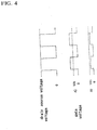
- FIG. 3 is a system configuration diagram of a motor drive device according to Embodiment 2 of the present invention.
- FIG. 4 is a voltage waveform diagram for supplementarily explaining details of Embodiment 2.
- a parasitic capacitance Cgd attributable to semiconductor structure exists between the gate G and the drain D inside a transistor Q8.
- switching pulses generated, by driving the transistor Q7, at the drain D side of the transistor Q8 are superimposed on the gate G side of the transistor Q8 through AC coupling by the parasitic capacitance between gate and drain Cgd. If the voltage between gate and source exceeds a threshold voltage Vth at which the transistor Q8 turns on, the transistor Q8 is brought into an on-state regardless of the drive signal path being open, thereby causing a short-circuit current and sometimes leading to transistor breakdown.
- Embodiment 2 of the present invention since a capacitor between gate and source Cgs is connected between the gate and source of the transistor Q8 as shown in FIG. 3 , the pulse voltage superimposed on the gate G becomes a value of the switching pulse voltage at the drain D side being capacitively divided by the parasitic capacitance between gate and drain Cgd and the capacitance of the capacitor between gate and source Cgs.
- the maximum pulse voltage generated at the drain D side of the transistor Q8 is equal to the voltage of the power supply 2
- the capacitor between gate and source Cgs is connected therebetween with its capacitance set to larger than a certain value, taking into consideration the maximum power supply voltage and the parasitic capacitance between gate and drain Cgd, the voltage between the gate and source of the transistor Q8 can be prevented from exceeding the threshold voltage Vth to turn on the transistor.
- FIG. 5 is a connection diagram for explaining the internal configuration of the transistors described in FIG. 3 of Embodiment 2.
- a transistor Q10 representing each of the transistors includes in its inside the semiconductor chip 5, and the bonding wire 7 connects the gate portion 8 on the semiconductor chip 5 with the gate terminal 6 of the transistor.
- the capacitor between gate and source Cgs is directly formed and disposed on the semiconductor chip 5, even when an open-circuit failure occurs at the gate terminal 6, the bonding wire 7 and the gate portion 8 on the semiconductor chip 5, which constitute the drive signal path inside the transistor Q10, the capacitor between gate and source Cgs remains in the connected state on the semiconductor chip; therefore, the capacitor can effectively fulfill its function so that the transistor Q10 can be brought into the off-state.
- Embodiment 2 of the present invention by configuring the transistor of the motor drive circuit with the capacitor between gate and source disposed inside the transistor, the transistor can be brought into the off-state without fail even when an open-circuit failure occurs, similarly to Embodiment1, in the drive signal path on the substrate. Moreover, there is no need for additionally providing extra parts outside, thereby enabling reduction in the number of parts and downsizing of the device.
- the capacitor between gate and source is structurally formed and disposed on the semiconductor chip itself as well as side the transistor, whereby the transistor can be brought into the off-state without fail even when an open-circuit failure occurs not only in the drive signal path on the substrate but also at the junctions inside the transistors.
- Embodiment 1 and Embodiment 2 are combined with each other and implemented in the motor drive device 1 that uses the motor drive circuit 3 made up of the upper and lower arms (transistors) as shown in FIG. 1 and FIG. 3 , which can prevent an excessive current caused by short-circuiting of both of the upper and lower arms due to an open-circuit failure in the drive signal path, whereby the motor drive device of a system and a power supply, a power line and a fuse connected to the device can be prevented from breaking down, disconnecting and heating up caused by the excessive current, thereby enhancing safety.
- the motor drive device of a system and a power supply, a power line and a fuse connected to the device can be prevented from breaking down, disconnecting and heating up caused by the excessive current, thereby enhancing safety.
- the whole of or a part of the circuit of the motor drive device 1 explained in Embodiment 1 to Embodiment 3 described above is sealed off with resin mold, thereby preventing wire disconnection and deterioration by the external environment. At least the resistor or the capacitors connected between the gate and source are sealed off with the resin mold, whereby reliability and durability of the device can be enhanced.
Landscapes
- Engineering & Computer Science (AREA)
- Power Engineering (AREA)
- Inverter Devices (AREA)
- Power Conversion In General (AREA)
- Electronic Switches (AREA)
- Control Of Ac Motors In General (AREA)
Applications Claiming Priority (1)
| Application Number | Priority Date | Filing Date | Title |
|---|---|---|---|
| JP2010248552A JP5161949B2 (ja) | 2010-11-05 | 2010-11-05 | モータ駆動装置 |
Publications (3)
| Publication Number | Publication Date |
|---|---|
| EP2451068A2 true EP2451068A2 (de) | 2012-05-09 |
| EP2451068A3 EP2451068A3 (de) | 2014-07-30 |
| EP2451068B1 EP2451068B1 (de) | 2020-03-11 |
Family
ID=45688311
Family Applications (1)
| Application Number | Title | Priority Date | Filing Date |
|---|---|---|---|
| EP11158797.8A Active EP2451068B1 (de) | 2010-11-05 | 2011-03-18 | Motorantriebsvorrichtung |
Country Status (2)
| Country | Link |
|---|---|
| EP (1) | EP2451068B1 (de) |
| JP (1) | JP5161949B2 (de) |
Family Cites Families (10)
| Publication number | Priority date | Publication date | Assignee | Title |
|---|---|---|---|---|
| JPH0879036A (ja) * | 1994-08-31 | 1996-03-22 | Oki Electric Ind Co Ltd | スイッチ回路 |
| JP2000299926A (ja) * | 1999-02-12 | 2000-10-24 | Yazaki Corp | 電源供給制御装置および電源供給制御方法 |
| JP2000299924A (ja) * | 1999-02-14 | 2000-10-24 | Yazaki Corp | 電源供給制御装置及び方法 |
| JP4547231B2 (ja) * | 2004-10-22 | 2010-09-22 | 日立オートモティブシステムズ株式会社 | 電力変換装置 |
| US7660094B2 (en) * | 2004-12-14 | 2010-02-09 | Mitsubishi Denki Kabushiki Kaisha | Inverter circuit |
| JP4916860B2 (ja) * | 2006-12-08 | 2012-04-18 | ルネサスエレクトロニクス株式会社 | 負荷駆動回路および負荷駆動回路の製造方法 |
| JP2008187066A (ja) * | 2007-01-31 | 2008-08-14 | Oki Electric Ind Co Ltd | パワートランジスタ |
| JP4453776B2 (ja) * | 2007-11-14 | 2010-04-21 | 株式会社デンソー | バススイッチ |
| JP5315026B2 (ja) * | 2008-11-28 | 2013-10-16 | ルネサスエレクトロニクス株式会社 | 半導体装置 |
| WO2011111208A1 (ja) * | 2010-03-11 | 2011-09-15 | 三菱電機株式会社 | 電力変換装置 |
-
2010
- 2010-11-05 JP JP2010248552A patent/JP5161949B2/ja not_active Expired - Fee Related
-
2011
- 2011-03-18 EP EP11158797.8A patent/EP2451068B1/de active Active
Non-Patent Citations (1)
| Title |
|---|
| None |
Also Published As
| Publication number | Publication date |
|---|---|
| JP2012100506A (ja) | 2012-05-24 |
| EP2451068B1 (de) | 2020-03-11 |
| EP2451068A3 (de) | 2014-07-30 |
| JP5161949B2 (ja) | 2013-03-13 |
Similar Documents
| Publication | Publication Date | Title |
|---|---|---|
| US7538587B2 (en) | Power semiconductor device | |
| CN104604134B (zh) | 半导体装置 | |
| CN103944548B (zh) | 用于晶体管的栅极驱动电路 | |
| JP6819256B2 (ja) | 駆動回路及び該回路を含んでなる半導体モジュール | |
| US9331188B2 (en) | Short-circuit protection circuits, system, and method | |
| CN104170238A (zh) | 变换器装置以及动力转向装置 | |
| US20130188287A1 (en) | Protection circuit, charge control circuit, and reverse current prevention method employing charge control circuit | |
| JP4339872B2 (ja) | 半導体素子駆動装置、電力変換装置、及びモータ駆動装置、並びに半導体素子駆動方法、電力変換方法、及びモータ駆動方法 | |
| US9859794B2 (en) | Semiconductor device and motor control unit | |
| JP2018011467A (ja) | 半導体スイッチング素子のゲート駆動回路 | |
| EP3104527B1 (de) | Halbleiterbauelement | |
| EP3010137B1 (de) | Mehrstufiger wechselrichter | |
| US9444446B2 (en) | Switching control circuit for target switching element | |
| US11721696B2 (en) | Semiconductor integrated circuit, motor driver, and motor drive system | |
| JP2018061301A (ja) | 半導体駆動装置ならびにそれを用いた電力変換装置 | |
| JP7589513B2 (ja) | 半導体装置 | |
| JP2019022253A (ja) | 半導体駆動装置およびこれを搭載した3相交流インバータ | |
| CN111527684B (zh) | 驱动电路内置型功率模块 | |
| JPWO2012043146A1 (ja) | 半導体装置 | |
| CN115189555B (zh) | 上臂驱动电路、电力转换装置的驱动电路、电力转换装置 | |
| WO2014099729A1 (en) | Gate drive circuits that control electromagnetic interference and switching losses and related methods | |
| CN115882838A (zh) | 半导体器件 | |
| EP2451068A2 (de) | Motorantriebsvorrichtung | |
| US12341500B2 (en) | Drive device for voltage-controlled semiconductor element | |
| JP6753348B2 (ja) | スイッチング素子の駆動回路 |
Legal Events
| Date | Code | Title | Description |
|---|---|---|---|
| PUAI | Public reference made under article 153(3) epc to a published international application that has entered the european phase |
Free format text: ORIGINAL CODE: 0009012 |
|
| 17P | Request for examination filed |
Effective date: 20110318 |
|
| AK | Designated contracting states |
Kind code of ref document: A2 Designated state(s): AL AT BE BG CH CY CZ DE DK EE ES FI FR GB GR HR HU IE IS IT LI LT LU LV MC MK MT NL NO PL PT RO RS SE SI SK SM TR |
|
| AX | Request for extension of the european patent |
Extension state: BA ME |
|
| PUAL | Search report despatched |
Free format text: ORIGINAL CODE: 0009013 |
|
| AK | Designated contracting states |
Kind code of ref document: A3 Designated state(s): AL AT BE BG CH CY CZ DE DK EE ES FI FR GB GR HR HU IE IS IT LI LT LU LV MC MK MT NL NO PL PT RO RS SE SI SK SM TR |
|
| AX | Request for extension of the european patent |
Extension state: BA ME |
|
| RIC1 | Information provided on ipc code assigned before grant |
Ipc: H02M 7/00 20060101AFI20140626BHEP |
|
| GRAP | Despatch of communication of intention to grant a patent |
Free format text: ORIGINAL CODE: EPIDOSNIGR1 |
|
| STAA | Information on the status of an ep patent application or granted ep patent |
Free format text: STATUS: GRANT OF PATENT IS INTENDED |
|
| INTG | Intention to grant announced |
Effective date: 20191119 |
|
| GRAS | Grant fee paid |
Free format text: ORIGINAL CODE: EPIDOSNIGR3 |
|
| GRAA | (expected) grant |
Free format text: ORIGINAL CODE: 0009210 |
|
| STAA | Information on the status of an ep patent application or granted ep patent |
Free format text: STATUS: THE PATENT HAS BEEN GRANTED |
|
| AK | Designated contracting states |
Kind code of ref document: B1 Designated state(s): AL AT BE BG CH CY CZ DE DK EE ES FI FR GB GR HR HU IE IS IT LI LT LU LV MC MK MT NL NO PL PT RO RS SE SI SK SM TR |
|
| REG | Reference to a national code |
Ref country code: GB Ref legal event code: FG4D |
|
| REG | Reference to a national code |
Ref country code: CH Ref legal event code: EP |
|
| REG | Reference to a national code |
Ref country code: AT Ref legal event code: REF Ref document number: 1244406 Country of ref document: AT Kind code of ref document: T Effective date: 20200315 |
|
| REG | Reference to a national code |
Ref country code: DE Ref legal event code: R096 Ref document number: 602011065470 Country of ref document: DE |
|
| REG | Reference to a national code |
Ref country code: IE Ref legal event code: FG4D |
|
| PG25 | Lapsed in a contracting state [announced via postgrant information from national office to epo] |
Ref country code: NO Free format text: LAPSE BECAUSE OF FAILURE TO SUBMIT A TRANSLATION OF THE DESCRIPTION OR TO PAY THE FEE WITHIN THE PRESCRIBED TIME-LIMIT Effective date: 20200611 Ref country code: RS Free format text: LAPSE BECAUSE OF FAILURE TO SUBMIT A TRANSLATION OF THE DESCRIPTION OR TO PAY THE FEE WITHIN THE PRESCRIBED TIME-LIMIT Effective date: 20200311 Ref country code: FI Free format text: LAPSE BECAUSE OF FAILURE TO SUBMIT A TRANSLATION OF THE DESCRIPTION OR TO PAY THE FEE WITHIN THE PRESCRIBED TIME-LIMIT Effective date: 20200311 |
|
| REG | Reference to a national code |
Ref country code: NL Ref legal event code: MP Effective date: 20200311 |
|
| PG25 | Lapsed in a contracting state [announced via postgrant information from national office to epo] |
Ref country code: LV Free format text: LAPSE BECAUSE OF FAILURE TO SUBMIT A TRANSLATION OF THE DESCRIPTION OR TO PAY THE FEE WITHIN THE PRESCRIBED TIME-LIMIT Effective date: 20200311 Ref country code: SE Free format text: LAPSE BECAUSE OF FAILURE TO SUBMIT A TRANSLATION OF THE DESCRIPTION OR TO PAY THE FEE WITHIN THE PRESCRIBED TIME-LIMIT Effective date: 20200311 Ref country code: HR Free format text: LAPSE BECAUSE OF FAILURE TO SUBMIT A TRANSLATION OF THE DESCRIPTION OR TO PAY THE FEE WITHIN THE PRESCRIBED TIME-LIMIT Effective date: 20200311 Ref country code: BG Free format text: LAPSE BECAUSE OF FAILURE TO SUBMIT A TRANSLATION OF THE DESCRIPTION OR TO PAY THE FEE WITHIN THE PRESCRIBED TIME-LIMIT Effective date: 20200611 Ref country code: GR Free format text: LAPSE BECAUSE OF FAILURE TO SUBMIT A TRANSLATION OF THE DESCRIPTION OR TO PAY THE FEE WITHIN THE PRESCRIBED TIME-LIMIT Effective date: 20200612 |
|
| REG | Reference to a national code |
Ref country code: LT Ref legal event code: MG4D |
|
| PG25 | Lapsed in a contracting state [announced via postgrant information from national office to epo] |
Ref country code: NL Free format text: LAPSE BECAUSE OF FAILURE TO SUBMIT A TRANSLATION OF THE DESCRIPTION OR TO PAY THE FEE WITHIN THE PRESCRIBED TIME-LIMIT Effective date: 20200311 |
|
| PG25 | Lapsed in a contracting state [announced via postgrant information from national office to epo] |
Ref country code: LT Free format text: LAPSE BECAUSE OF FAILURE TO SUBMIT A TRANSLATION OF THE DESCRIPTION OR TO PAY THE FEE WITHIN THE PRESCRIBED TIME-LIMIT Effective date: 20200311 Ref country code: IS Free format text: LAPSE BECAUSE OF FAILURE TO SUBMIT A TRANSLATION OF THE DESCRIPTION OR TO PAY THE FEE WITHIN THE PRESCRIBED TIME-LIMIT Effective date: 20200711 Ref country code: CZ Free format text: LAPSE BECAUSE OF FAILURE TO SUBMIT A TRANSLATION OF THE DESCRIPTION OR TO PAY THE FEE WITHIN THE PRESCRIBED TIME-LIMIT Effective date: 20200311 Ref country code: RO Free format text: LAPSE BECAUSE OF FAILURE TO SUBMIT A TRANSLATION OF THE DESCRIPTION OR TO PAY THE FEE WITHIN THE PRESCRIBED TIME-LIMIT Effective date: 20200311 Ref country code: SK Free format text: LAPSE BECAUSE OF FAILURE TO SUBMIT A TRANSLATION OF THE DESCRIPTION OR TO PAY THE FEE WITHIN THE PRESCRIBED TIME-LIMIT Effective date: 20200311 Ref country code: SM Free format text: LAPSE BECAUSE OF FAILURE TO SUBMIT A TRANSLATION OF THE DESCRIPTION OR TO PAY THE FEE WITHIN THE PRESCRIBED TIME-LIMIT Effective date: 20200311 Ref country code: EE Free format text: LAPSE BECAUSE OF FAILURE TO SUBMIT A TRANSLATION OF THE DESCRIPTION OR TO PAY THE FEE WITHIN THE PRESCRIBED TIME-LIMIT Effective date: 20200311 Ref country code: PT Free format text: LAPSE BECAUSE OF FAILURE TO SUBMIT A TRANSLATION OF THE DESCRIPTION OR TO PAY THE FEE WITHIN THE PRESCRIBED TIME-LIMIT Effective date: 20200805 |
|
| REG | Reference to a national code |
Ref country code: CH Ref legal event code: PL |
|
| REG | Reference to a national code |
Ref country code: AT Ref legal event code: MK05 Ref document number: 1244406 Country of ref document: AT Kind code of ref document: T Effective date: 20200311 |
|
| REG | Reference to a national code |
Ref country code: DE Ref legal event code: R097 Ref document number: 602011065470 Country of ref document: DE |
|
| REG | Reference to a national code |
Ref country code: BE Ref legal event code: MM Effective date: 20200331 |
|
| PG25 | Lapsed in a contracting state [announced via postgrant information from national office to epo] |
Ref country code: LU Free format text: LAPSE BECAUSE OF NON-PAYMENT OF DUE FEES Effective date: 20200318 Ref country code: MC Free format text: LAPSE BECAUSE OF FAILURE TO SUBMIT A TRANSLATION OF THE DESCRIPTION OR TO PAY THE FEE WITHIN THE PRESCRIBED TIME-LIMIT Effective date: 20200311 |
|
| PLBE | No opposition filed within time limit |
Free format text: ORIGINAL CODE: 0009261 |
|
| STAA | Information on the status of an ep patent application or granted ep patent |
Free format text: STATUS: NO OPPOSITION FILED WITHIN TIME LIMIT |
|
| PG25 | Lapsed in a contracting state [announced via postgrant information from national office to epo] |
Ref country code: ES Free format text: LAPSE BECAUSE OF FAILURE TO SUBMIT A TRANSLATION OF THE DESCRIPTION OR TO PAY THE FEE WITHIN THE PRESCRIBED TIME-LIMIT Effective date: 20200311 Ref country code: AT Free format text: LAPSE BECAUSE OF FAILURE TO SUBMIT A TRANSLATION OF THE DESCRIPTION OR TO PAY THE FEE WITHIN THE PRESCRIBED TIME-LIMIT Effective date: 20200311 Ref country code: IT Free format text: LAPSE BECAUSE OF FAILURE TO SUBMIT A TRANSLATION OF THE DESCRIPTION OR TO PAY THE FEE WITHIN THE PRESCRIBED TIME-LIMIT Effective date: 20200311 Ref country code: IE Free format text: LAPSE BECAUSE OF NON-PAYMENT OF DUE FEES Effective date: 20200318 Ref country code: DK Free format text: LAPSE BECAUSE OF FAILURE TO SUBMIT A TRANSLATION OF THE DESCRIPTION OR TO PAY THE FEE WITHIN THE PRESCRIBED TIME-LIMIT Effective date: 20200311 Ref country code: LI Free format text: LAPSE BECAUSE OF NON-PAYMENT OF DUE FEES Effective date: 20200331 Ref country code: CH Free format text: LAPSE BECAUSE OF NON-PAYMENT OF DUE FEES Effective date: 20200331 |
|
| 26N | No opposition filed |
Effective date: 20201214 |
|
| PG25 | Lapsed in a contracting state [announced via postgrant information from national office to epo] |
Ref country code: BE Free format text: LAPSE BECAUSE OF NON-PAYMENT OF DUE FEES Effective date: 20200331 Ref country code: SI Free format text: LAPSE BECAUSE OF FAILURE TO SUBMIT A TRANSLATION OF THE DESCRIPTION OR TO PAY THE FEE WITHIN THE PRESCRIBED TIME-LIMIT Effective date: 20200311 Ref country code: PL Free format text: LAPSE BECAUSE OF FAILURE TO SUBMIT A TRANSLATION OF THE DESCRIPTION OR TO PAY THE FEE WITHIN THE PRESCRIBED TIME-LIMIT Effective date: 20200311 |
|
| GBPC | Gb: european patent ceased through non-payment of renewal fee |
Effective date: 20200611 |
|
| PG25 | Lapsed in a contracting state [announced via postgrant information from national office to epo] |
Ref country code: GB Free format text: LAPSE BECAUSE OF NON-PAYMENT OF DUE FEES Effective date: 20200611 |
|
| PG25 | Lapsed in a contracting state [announced via postgrant information from national office to epo] |
Ref country code: TR Free format text: LAPSE BECAUSE OF FAILURE TO SUBMIT A TRANSLATION OF THE DESCRIPTION OR TO PAY THE FEE WITHIN THE PRESCRIBED TIME-LIMIT Effective date: 20200311 Ref country code: MT Free format text: LAPSE BECAUSE OF FAILURE TO SUBMIT A TRANSLATION OF THE DESCRIPTION OR TO PAY THE FEE WITHIN THE PRESCRIBED TIME-LIMIT Effective date: 20200311 Ref country code: CY Free format text: LAPSE BECAUSE OF FAILURE TO SUBMIT A TRANSLATION OF THE DESCRIPTION OR TO PAY THE FEE WITHIN THE PRESCRIBED TIME-LIMIT Effective date: 20200311 |
|
| PG25 | Lapsed in a contracting state [announced via postgrant information from national office to epo] |
Ref country code: MK Free format text: LAPSE BECAUSE OF FAILURE TO SUBMIT A TRANSLATION OF THE DESCRIPTION OR TO PAY THE FEE WITHIN THE PRESCRIBED TIME-LIMIT Effective date: 20200311 Ref country code: AL Free format text: LAPSE BECAUSE OF FAILURE TO SUBMIT A TRANSLATION OF THE DESCRIPTION OR TO PAY THE FEE WITHIN THE PRESCRIBED TIME-LIMIT Effective date: 20200311 |
|
| PGFP | Annual fee paid to national office [announced via postgrant information from national office to epo] |
Ref country code: FR Payment date: 20230208 Year of fee payment: 13 |
|
| PGFP | Annual fee paid to national office [announced via postgrant information from national office to epo] |
Ref country code: DE Payment date: 20230131 Year of fee payment: 13 |
|
| P01 | Opt-out of the competence of the unified patent court (upc) registered |
Effective date: 20230512 |
|
| REG | Reference to a national code |
Ref country code: DE Ref legal event code: R119 Ref document number: 602011065470 Country of ref document: DE |
|
| PG25 | Lapsed in a contracting state [announced via postgrant information from national office to epo] |
Ref country code: DE Free format text: LAPSE BECAUSE OF NON-PAYMENT OF DUE FEES Effective date: 20241001 |
|
| PG25 | Lapsed in a contracting state [announced via postgrant information from national office to epo] |
Ref country code: FR Free format text: LAPSE BECAUSE OF NON-PAYMENT OF DUE FEES Effective date: 20240331 |
|
| PG25 | Lapsed in a contracting state [announced via postgrant information from national office to epo] |
Ref country code: FR Free format text: LAPSE BECAUSE OF NON-PAYMENT OF DUE FEES Effective date: 20240331 Ref country code: DE Free format text: LAPSE BECAUSE OF NON-PAYMENT OF DUE FEES Effective date: 20241001 |