EP2455931A1 - Abtastsignal-anlagenantriebsschaltung und anzeigevorrichtung damit - Google Patents
Abtastsignal-anlagenantriebsschaltung und anzeigevorrichtung damit Download PDFInfo
- Publication number
- EP2455931A1 EP2455931A1 EP10799655A EP10799655A EP2455931A1 EP 2455931 A1 EP2455931 A1 EP 2455931A1 EP 10799655 A EP10799655 A EP 10799655A EP 10799655 A EP10799655 A EP 10799655A EP 2455931 A1 EP2455931 A1 EP 2455931A1
- Authority
- EP
- European Patent Office
- Prior art keywords
- stage
- shift register
- clock
- clock signals
- scanning signal
- Prior art date
- Legal status (The legal status is an assumption and is not a legal conclusion. Google has not performed a legal analysis and makes no representation as to the accuracy of the status listed.)
- Withdrawn
Links
- 239000010409 thin film Substances 0.000 description 74
- 238000010586 diagram Methods 0.000 description 43
- 239000004973 liquid crystal related substance Substances 0.000 description 22
- 230000015572 biosynthetic process Effects 0.000 description 10
- 239000010408 film Substances 0.000 description 10
- 230000000694 effects Effects 0.000 description 9
- 201000005569 Gout Diseases 0.000 description 8
- 229910021424 microcrystalline silicon Inorganic materials 0.000 description 7
- 229910021417 amorphous silicon Inorganic materials 0.000 description 4
- 239000003990 capacitor Substances 0.000 description 4
- 230000007423 decrease Effects 0.000 description 4
- 230000003247 decreasing effect Effects 0.000 description 4
- 239000011159 matrix material Substances 0.000 description 4
- 102100027241 Adenylyl cyclase-associated protein 1 Human genes 0.000 description 3
- 108010077333 CAP1-6D Proteins 0.000 description 3
- 238000005401 electroluminescence Methods 0.000 description 3
- 230000003071 parasitic effect Effects 0.000 description 3
- 108010031970 prostasin Proteins 0.000 description 3
- 239000000758 substrate Substances 0.000 description 3
- 239000007789 gas Substances 0.000 description 2
- 239000011521 glass Substances 0.000 description 2
- 238000009413 insulation Methods 0.000 description 2
- 238000004519 manufacturing process Methods 0.000 description 2
- 239000003566 sealing material Substances 0.000 description 2
- 239000004065 semiconductor Substances 0.000 description 2
- UFHFLCQGNIYNRP-UHFFFAOYSA-N Hydrogen Chemical compound [H][H] UFHFLCQGNIYNRP-UHFFFAOYSA-N 0.000 description 1
- BLRPTPMANUNPDV-UHFFFAOYSA-N Silane Chemical compound [SiH4] BLRPTPMANUNPDV-UHFFFAOYSA-N 0.000 description 1
- 208000000260 Warts Diseases 0.000 description 1
- 238000005229 chemical vapour deposition Methods 0.000 description 1
- 230000001934 delay Effects 0.000 description 1
- 238000000375 direct analysis in real time Methods 0.000 description 1
- 238000012063 dual-affinity re-targeting Methods 0.000 description 1
- 239000000463 material Substances 0.000 description 1
- 238000000034 method Methods 0.000 description 1
- 238000005268 plasma chemical vapour deposition Methods 0.000 description 1
- 229910000077 silane Inorganic materials 0.000 description 1
- 201000010153 skin papilloma Diseases 0.000 description 1
Images







Classifications
-
- G—PHYSICS
- G09—EDUCATION; CRYPTOGRAPHY; DISPLAY; ADVERTISING; SEALS
- G09G—ARRANGEMENTS OR CIRCUITS FOR CONTROL OF INDICATING DEVICES USING STATIC MEANS TO PRESENT VARIABLE INFORMATION
- G09G3/00—Control arrangements or circuits, of interest only in connection with visual indicators other than cathode-ray tubes
- G09G3/20—Control arrangements or circuits, of interest only in connection with visual indicators other than cathode-ray tubes for presentation of an assembly of a number of characters, e.g. a page, by composing the assembly by combination of individual elements arranged in a matrix no fixed position being assigned to or needed to be assigned to the individual characters or partial characters
- G09G3/34—Control arrangements or circuits, of interest only in connection with visual indicators other than cathode-ray tubes for presentation of an assembly of a number of characters, e.g. a page, by composing the assembly by combination of individual elements arranged in a matrix no fixed position being assigned to or needed to be assigned to the individual characters or partial characters by control of light from an independent source
- G09G3/36—Control arrangements or circuits, of interest only in connection with visual indicators other than cathode-ray tubes for presentation of an assembly of a number of characters, e.g. a page, by composing the assembly by combination of individual elements arranged in a matrix no fixed position being assigned to or needed to be assigned to the individual characters or partial characters by control of light from an independent source using liquid crystals
- G09G3/3611—Control of matrices with row and column drivers
- G09G3/3674—Details of drivers for scan electrodes
- G09G3/3677—Details of drivers for scan electrodes suitable for active matrices only
-
- G—PHYSICS
- G11—INFORMATION STORAGE
- G11C—STATIC STORES
- G11C19/00—Digital stores in which the information is moved stepwise, e.g. shift registers
- G11C19/18—Digital stores in which the information is moved stepwise, e.g. shift registers using capacitors as main elements of the stages
- G11C19/182—Digital stores in which the information is moved stepwise, e.g. shift registers using capacitors as main elements of the stages in combination with semiconductor elements, e.g. bipolar transistors, diodes
- G11C19/184—Digital stores in which the information is moved stepwise, e.g. shift registers using capacitors as main elements of the stages in combination with semiconductor elements, e.g. bipolar transistors, diodes with field-effect transistors, e.g. MOS-FET
-
- G—PHYSICS
- G11—INFORMATION STORAGE
- G11C—STATIC STORES
- G11C19/00—Digital stores in which the information is moved stepwise, e.g. shift registers
- G11C19/28—Digital stores in which the information is moved stepwise, e.g. shift registers using semiconductor elements
-
- G—PHYSICS
- G02—OPTICS
- G02F—OPTICAL DEVICES OR ARRANGEMENTS FOR THE CONTROL OF LIGHT BY MODIFICATION OF THE OPTICAL PROPERTIES OF THE MEDIA OF THE ELEMENTS INVOLVED THEREIN; NON-LINEAR OPTICS; FREQUENCY-CHANGING OF LIGHT; OPTICAL LOGIC ELEMENTS; OPTICAL ANALOGUE/DIGITAL CONVERTERS
- G02F1/00—Devices or arrangements for the control of the intensity, colour, phase, polarisation or direction of light arriving from an independent light source, e.g. switching, gating or modulating; Non-linear optics
- G02F1/01—Devices or arrangements for the control of the intensity, colour, phase, polarisation or direction of light arriving from an independent light source, e.g. switching, gating or modulating; Non-linear optics for the control of the intensity, phase, polarisation or colour
- G02F1/13—Devices or arrangements for the control of the intensity, colour, phase, polarisation or direction of light arriving from an independent light source, e.g. switching, gating or modulating; Non-linear optics for the control of the intensity, phase, polarisation or colour based on liquid crystals, e.g. single liquid crystal display cells
- G02F1/133—Constructional arrangements; Operation of liquid crystal cells; Circuit arrangements
- G02F1/1333—Constructional arrangements; Manufacturing methods
- G02F1/1345—Conductors connecting electrodes to cell terminals
- G02F1/13454—Drivers integrated on the active matrix substrate
-
- G—PHYSICS
- G09—EDUCATION; CRYPTOGRAPHY; DISPLAY; ADVERTISING; SEALS
- G09G—ARRANGEMENTS OR CIRCUITS FOR CONTROL OF INDICATING DEVICES USING STATIC MEANS TO PRESENT VARIABLE INFORMATION
- G09G2310/00—Command of the display device
- G09G2310/02—Addressing, scanning or driving the display screen or processing steps related thereto
- G09G2310/0264—Details of driving circuits
- G09G2310/0267—Details of drivers for scan electrodes, other than drivers for liquid crystal, plasma or OLED displays
-
- G—PHYSICS
- G09—EDUCATION; CRYPTOGRAPHY; DISPLAY; ADVERTISING; SEALS
- G09G—ARRANGEMENTS OR CIRCUITS FOR CONTROL OF INDICATING DEVICES USING STATIC MEANS TO PRESENT VARIABLE INFORMATION
- G09G2310/00—Command of the display device
- G09G2310/02—Addressing, scanning or driving the display screen or processing steps related thereto
- G09G2310/0264—Details of driving circuits
- G09G2310/0286—Details of a shift registers arranged for use in a driving circuit
-
- G—PHYSICS
- G09—EDUCATION; CRYPTOGRAPHY; DISPLAY; ADVERTISING; SEALS
- G09G—ARRANGEMENTS OR CIRCUITS FOR CONTROL OF INDICATING DEVICES USING STATIC MEANS TO PRESENT VARIABLE INFORMATION
- G09G3/00—Control arrangements or circuits, of interest only in connection with visual indicators other than cathode-ray tubes
- G09G3/20—Control arrangements or circuits, of interest only in connection with visual indicators other than cathode-ray tubes for presentation of an assembly of a number of characters, e.g. a page, by composing the assembly by combination of individual elements arranged in a matrix no fixed position being assigned to or needed to be assigned to the individual characters or partial characters
- G09G3/22—Control arrangements or circuits, of interest only in connection with visual indicators other than cathode-ray tubes for presentation of an assembly of a number of characters, e.g. a page, by composing the assembly by combination of individual elements arranged in a matrix no fixed position being assigned to or needed to be assigned to the individual characters or partial characters using controlled light sources
- G09G3/30—Control arrangements or circuits, of interest only in connection with visual indicators other than cathode-ray tubes for presentation of an assembly of a number of characters, e.g. a page, by composing the assembly by combination of individual elements arranged in a matrix no fixed position being assigned to or needed to be assigned to the individual characters or partial characters using controlled light sources using electroluminescent panels
- G09G3/32—Control arrangements or circuits, of interest only in connection with visual indicators other than cathode-ray tubes for presentation of an assembly of a number of characters, e.g. a page, by composing the assembly by combination of individual elements arranged in a matrix no fixed position being assigned to or needed to be assigned to the individual characters or partial characters using controlled light sources using electroluminescent panels semiconductive, e.g. using light-emitting diodes [LED]
- G09G3/3208—Control arrangements or circuits, of interest only in connection with visual indicators other than cathode-ray tubes for presentation of an assembly of a number of characters, e.g. a page, by composing the assembly by combination of individual elements arranged in a matrix no fixed position being assigned to or needed to be assigned to the individual characters or partial characters using controlled light sources using electroluminescent panels semiconductive, e.g. using light-emitting diodes [LED] organic, e.g. using organic light-emitting diodes [OLED]
- G09G3/3266—Details of drivers for scan electrodes
Definitions
- the present invention relates to a scanning signal line drive circuit of an active matrix-type display device, and in particular to a shift register included in a scanning signal line drive circuit.
- an active matrix-type display device in which a plurality of gate bus lines (scanning signal lines) and a plurality of source bus lines (video signal lines) are provided in a grid pattern, and a plurality of pixel formation portions are provided in matrix corresponding to respective intersection points between the signal lines.
- Each pixel formation portion includes a thin film transistor (Thin Film Transistor: TFT) as a switching device and a pixel capacitance for holding a pixel value.
- TFT Thin Film Transistor
- a gate terminal of the thin film transistor is connected to the gate bus line that passes the corresponding intersection point, and a source terminal of the thin film transistor is connected to the source bus line that passes the same intersection point.
- the active matrix-type display device is further provided with a gate driver (scanning signal line drive circuit) that drives the gate bus lines and a source driver (video signal line drive circuit) that drives the source bus lines.
- Video signals indicating the pixel values are transmitted through the source bus lines, but a single source bus line cannot transmit video signals indicating the pixel values of more than one row at the same time (simultaneously) . Accordingly, the video signals are written to the pixel capacitances included in the pixel formation portions sequentially by row.
- a gate driver including a shift register having a plurality of stages is used to sequentially select the plurality of gate bus lines for a predetermined time period.
- the shift register operates based on clock signals.
- the clock signals are supplied to each stage of the shift register from clock signal main lines provided on an outer rim of a panel. Further, the clock signals are typically supplied to a plurality of thin film transistors included in the shift register. Accordingly, an area for laying out the shift register is required between an area for providing the clock signal main lines and an area for providing the pixel formation portions. This constitutes one reason of an increase of the area for laying out the shift register. In particular, in a case of a display device having a shift register that operates based on a large number of clock signals, an increase of a picture-frame area of the panel becomes problematic.
- Patent Documents 1 to 7 disclose a structure of a gate driver including a shift register. According to these documents, clock signals necessary for an operation of the shift register are supplied to each stage of the shift register from clock signal main lines as shown in Fig. 26 .
- Patent Document 1 discloses decreasing an interval between signal lines of a gate driving unit by providing contacts (square boxes with diagonal lines) and zigzag leading lines to connect between main lines and each stage of the gate driving unit.
- Patent Document 7 discloses connecting clock leading lines from the clock signal main lines to two adjacent stages in a single shift register, and that the clock signals are shared by the two stages (see Figs. 4 and 6 of Patent Document 7).
- Patent Document 6 The same structure is also disclosed in Patent Document 6 (see Figs. 3 and 5 of Patent Document 6).
- the number of types of the clock signals required for the operation of the shift register is two (CK1 and CK2), and the number of clock leading lines is one for each stage of the shift register.
- Patent Document 1 discloses a structure of decreasing an interval between signal lines of a gate driving unit. In order to sufficiently protect the gate driving unit (gate driver), it is desirable that the gate driving unit be covered (concealed) by a liquid crystal panel sealing material. However, according to the structure disclosed by Patent Document 1, increasing the number of wire lines in the gate driving unit decreases an area for applying the sealing material, resulting in insufficient protection of the gate driving unit.
- Patent Documents 6 and 7 disclose a structure of decreasing the number of clock leading lines to be smaller than the number of clocks necessary for the operation of the shift register. These documents disclose a gate driving unit including a single shift register. However, it is difficult to drive a large size liquid crystal panel by a single shift register due to a large load, and two or more shift registers are required.
- an object of the present invention is to reduce a picture-frame area of a panel in a display device provided with a scanning signal line drive circuit having a plurality of shift registers (for example, a display device having a large size panel).
- a scanning signal line drive circuit capable of driving a plurality of scanning signal lines provided on a display unit of a display device, the scanning signal line drive circuit including: a plurality of shift registers each including a plurality of stages, and sequentially shifting a pulse supplied to a first stage based on a plurality of clock signals supplied to each stage to drive the scanning signal lines; and clock signal main lines including a plurality of signal lines respectively transmitting the clock signals, and provided on an opposite side of the display unit with respect to the shift registers, wherein each stage of the shift register receives a part of the clock signals from the clock signal main line, and a remaining part of the clock signals from another one of the shift registers.
- each stage of the shift register operates based on four clock signals.
- each stage of the shift register receives the remaining part of the clock signals from an adjacently provided stage of the other shift register.
- each stage of the shift register includes a charge control switching device configured to charge a corresponding one of the scanning signal lines based on the clock signal received from the clock signal main line, and a phase of the remaining part of the clock signals is displaced by 90 degrees from a phase of the clock signal supplied to the charge control switching device.
- each stage of the shift register includes a contact for supplying the part of the clock signals to both of a preceding-side and a succeeding-side stage of the other shift register.
- each stage of the shift register includes a contact for supplying the part of the clock signals to a preceding-side stage of the other shift register and a contact for supplying the part of the clock signals to a succeeding-side stage of the other shift register, the two contacts being provided at positions adjacent to each other.
- the plurality of the shift registers include a shift register having a dummy stage configured to supply the clock signal received from the clock signal main line to the first stage without change, and a shift register having a dummy stage configured to supply the clock signal received from the clock signal main line to a last stage without change.
- the dummy stage is configured only by a component necessary for transmitting the clock signal received from the clock signal main line, out of components of each stage of the shift register.
- a display device including: a display unit including a plurality of scanning signal lines; and the scanning signal line drive circuit according to one of the first to eighth aspects of the present invention.
- a scanning signal line drive circuit capable of driving a plurality of scanning signal lines provided on a display unit of a display device, the scanning signal line drive circuit including: a plurality of shift registers each including a plurality of stages, and sequentially shifting a pulse supplied to a first stage based on a plurality of clock signals supplied to each stage to drive the scanning signal lines; and clock signal main lines including a plurality of signal lines respectively transmitting the clock signals, and provided on an opposite side of the display unit with respect to the shift registers, wherein each stage of the shift register receives a part of the clock signals from the clock signal main line, a different part of the clock signals from another one of the shift registers, and a remaining part of the clock signals from a different stage of the same shift register.
- each stage of the shift register operates based on four clock signals.
- each stage of the shift register receives the different part of the clock signals from an adjacently provided stage of the other shift register, and the remaining part of the clock signals from one of a preceding stage and a succeeding stage of the same shift register.
- each stage of the shift register includes a charge control switching device configured to charge a corresponding one of the scanning signal lines based on the clock signal received from the clock signal main line, and a phase of the different part of the clock signals and a phase of the remaining part of the clock signals are displaced respectively by 90 degrees and 180 degrees from a phase of the clock signal supplied to the charge control switching device.
- each stage of the shift register includes a contact for supplying the part of the clock signals to at least two of a preceding-side stage of the other shift register, a succeeding-side stage of the other shift register, and a different stage of the same shift register.
- each stage of the shift register includes a contact for supplying the part of the clock signals to a preceding-side stage of the other shift register, a contact for supplying the part of the clock signals to a succeeding-side stage of the other shift register, and a contact for supplying the part of the clock signals to a different stage of the same shift register, at least two of the three contacts being provided at positions adjacent to each other.
- the plurality of the shift registers include a shift register having a dummy stage configured to supply the clock signal received from the clock signal main line to the first stage without change, and a shift register having a dummy stage configured to supply the clock signal received from the clock signal main line to a last stage without change.
- the dummy stage is configured only by a component necessary for transmitting the clock signal received from the clock signal main line, out of components of each stage of the shift register.
- a display device including: a display unit including a plurality of scanning signal lines; and the scanning signal line drive circuit according to one of the tenth to seventeenth aspects of the present invention.
- the number of wire lines connecting between the clock signal main lines and each stage of the shift register decreases as compared to the conventional example. Accordingly, an area for the clock signal lines in each stage of the shift register becomes smaller. Further, as a load capacitance per one of the clock signal main lines becomes smaller as compared to the conventional example, it is possible to suppress mutual interference between the clock signals, and to reduce waveform rounding in the clock signals. Therefore, as compared to the conventional example, it is possible to downsize switching devices (for example, thin film transistors) that constitute the shift register.
- the scanning signal line drive circuit provided with the shift registers operating based on the four clock signals provides the same effect as that of the first or tenth aspect.
- the third or twelfth aspect of the present invention it is possible to supply the clock signals to each stage of the shift register from a portion other than the clock signal main lines using relatively short signal lines. Accordingly, it is possible to achieve the scanning signal line drive circuit providing the same effect as that of the first or tenth aspect with a relatively simple configuration.
- the scanning signal line drive circuit provided with the shift registers operating based on the plurality of clock signals whose phases are displaced by 90 degrees to each other provides the same effect as that of the first or tenth aspect.
- configuring a part or all of the necessary contacts by a single contact reduces an area occupied by the contacts in each stage of the shift registers, and whereby the picture-frame area of the panel can be effectively reduced.
- the sixth or fifteenth aspect of the present invention it is possible to reduce a contact resistance as compared to a case in which the plurality of contacts are provided at distant positions.
- the stages of the shift registers have the same circuit configuration and parasitic capacitances become substantially equal, waveform rounding in the clock signals becomes substantially identical. This allows the shift registers to operate stably.
- the ninth or eighteenth aspect of the present invention it is possible to achieve the display device provided with the scanning signal line drive circuit providing the same effect as that of any of the first to eighth and the tenth to seventeenth aspects.
- Fig. 1 is a block diagram illustrating a configuration of a liquid crystal display device according to a first embodiment of the present invention.
- the liquid crystal display device shown in Fig. 1 is an active znatrix-type display device provided with a power supply 1, a DC/DC converter 2, a display control circuit 3, a gate driver (scanning signal line drive circuit) 4, a source driver (video signal line drive circuit) 5, a common electrode drive circuit 6, and a display unit 7.
- the gate driver 4 and the display unit 7 are formed monolithically on the same substrate.
- the liquid crystal display device according to this embodiment is characterized in a configuration of a shift register included in the gate driver 4.
- m is an even number
- n is an integer not smaller than 2
- m 2a.
- the display unit 7 includes m gate bus lines (scanning signal lines) GL1 to GLm, n source bus lines (video signal lines) SL1 to SLn, and (mxn) pixel formation portions provided corresponding to intersection points between these signal lines.
- the (mxn) pixel formation portions are provided in matrix and constitute a pixel array.
- Each pixel formation portion includes a thin film transistor 8 as a switching device, a pixel electrode, a common electrode Ec, and a liquid crystal layer.
- a gate terminal of the thin film transistor 8 is connected to one of the gate bus lines that passes the corresponding intersection point, a source terminal of the thin film transistor 8 is connected to one of the source bus lines that passes the same intersection point, and a drain terminal of the thin film transistor 8 is connected to the pixel electrode.
- the common electrode Ec is a counter electrode provided in common to the (mxn) pixel formation portions.
- the liquid crystal layer is sandwiched between the pixel electrode and the common electrode Ec.
- a pixel capacitance Cp is constituted by a liquid crystal capacitance formed by the pixel electrode and the common electrode Ec.
- auxiliary capacitance in parallel with the liquid crystal capacitance, in order to reliably hold a voltage in the pixel capacitance Cp.
- the auxiliary capacitance is not directly related to the present invention, and therefore an explanation and an illustration of the auxiliary capacitance are omitted.
- the power supply 1 supplies a predetermined power-supply voltage to the DC/DC converter 2, the display control circuit 3, and the common electrode drive circuit 6.
- the DC/DC converter 2 generates a predetermined direct-current voltage based on the power-supply voltage supplied from the power supply 1, and supplies the generated direct-current voltage to the gate driver 4 and the source driver 5.
- the common electrode drive circuit 6 supplies a predetermined potential Vcom to the common electrode Ec.
- the display control circuit 3 receives an image signal DAT and a group of timing signals TG (including such as a horizontal synchronization signal and a vertical synchronization signal) that are externally supplied, and outputs a digital video signal DV and control signals for controlling display of an image in the display unit 7.
- the control signals outputted from the display control circuit 3 include a source start pulse signal SSP, a source clock signal SCK, a latch strobe signal LS, a first gate start pulse signal GSP_O, a second gate start pulse signal GSP_E, a first gate end pulse signal GEP_O, a second gate end pulse signal GEP_E, and gate clock signals GCK.
- the gate clock signals GCK includes clock signals CK1, CKLB, CK2, and CK2B of four phases (hereinafter referred to as first to fourth gate clock signals) .
- the gate driver 4 receives the first gate start pulse signal GSP_O, the second gate start pulse signal GSP__E, the first gate end pulse signal GEP_O, the second gate end pulse signal GEP_E, and the gate clock signals GCK outputted from the display control circuit 3.
- the gate driver 4 repeats, based on these signals, an operation of sequentially applying active scanning signals Gout(1) to Gout(m) to the gate bus lines GL1 to GLm taking one vertical scanning period as a single cycle.
- the source driver 5 receives the digital video signal DV, the source start pulse signal SSP, the source clock signal SCK, and the latch strobe signal LS outputted from the display control circuit 3. The source driver 5 applies, based on these signals, driving video signals S (1) to S(n) to the source bus lines SL1 to SLn.
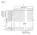
- Fig. 2 is a block diagram illustrating a schematic configuration of the gate driver 4.
- the gate driver 4 is formed with a shift register 10 having a plurality of stages.
- the display unit 7 is provided with a pixel matrix of m rows x n columns, and each stage of the shift register 10 corresponds to each row of the pixel matrix on a one-to-one basis.
- Each stage of the shift register 10 is configured as a bistable circuit 11.
- the bistable circuit 11 holds two states, and is turned to be in either of the states at any given time point, outputs a signal indicating this state (hereinafter referred to as a state signal).
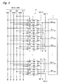
- Fig. 3 is a block diagram illustrating the gate driver 4 in detail.
- the gate driver 4 is provided with the shift register 10 including the m bistable circuits 11 and main lines including clock signal main lines.
- the shift register 10 is configured by arranging the m bistable circuits 11 in a vertical direction. Further, the shift register 10 is disposed on a left side of the display unit 7. On a left side of the shift register 10, the main lines for the first to fourth gate clock signals CK1, CK1B, CK2, and CK2B, the main line for a low-potential direct-current voltage VSS, and the main line for a clear signal CLR are disposed.
- clock signals CKA, CKB, CKC, and CKD of four phases (hereinafter referred to as first to fourth clocks), a set signal S, a reset signal R, the clear signal CLR, and the low-potential direct-current voltage VSS are inputted, and a state signal Q is outputted from the bistable circuit 11.
- the bistable circuit 11 outputs the inputted second clock CKB to neighboring stages (including an adjacent stage) as a clock signal for the neighboring stages (including the adjacent stage) in the shift register.
- the signals supplied to each stage (the bistable circuit 11) of the shift register 10 are stated below.
- the low-potential direct-current voltage VSS and the clear signal CLR are supplied to all the stages in common.
- k is an integer not smaller than 1 and not greater than a predetermined integer
- the bistable circuit of a (4k-3) th stage the first gate clock signal CK1 as the first clock CKA. and the second gate clock signal CK1B as the second clock CKB are supplied.
- the bistable circuit of a (4k-2)th stage the third gate clock signal CK2 as the first clock CKA and the fourth gate clock signal CK2B as the second clock CKB are supplied.
- the second gate clock signal CK1B as the first clock CKA and the first gate clock signal CK1 as the second clock CKB are supplied.
- the fourth gate clock signal CK2B as the first clock CKA and the third gate clock signal CK2 as the second clock CKB are supplied.
- Each stage of the shift register 10 receives the low-potential direct-current voltage VSS, the clear signal CLR, the first clock CKA, and the second clock CKB from the main lines.
- the first gate clock signal CK1 (when a is an odd number) or the second gate clock signal CK1B (when a is an even number) is supplied as the third clock CKC from the main line.
- Fig. 3 shows the case where a is an odd number.
- the second clock CKB outputted from a succeeding stage is supplied as the third clock CKC.
- the third gate clock signal CK2 is supplied as the fourth clock CKD from the main line.
- the second clock CKB outputted from a preceding stage is supplied as the fourth clock CKD.
- the first gate start pulse signal GSP_O is supplied as the set signal S.
- the second gate start pulse signal GSP_E is supplied as the set signal S.
- the state signal Q outputted from a second preceding stage is supplied as the set signal S.
- the second gate end pulse signal GEP_E is supplied as the reset signal R.
- the first gate end pulse signal GEP_O is supplied as the reset signal R.
- the state signal Q outputted from a second succeeding stage is supplied as the reset signal R.
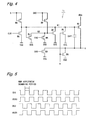
- Fig. 4 is a circuit diagram of the bistable circuit 11.
- the bistable circuit 11 includes ten thin film transistors MA, MB, MI, MF, MJ, MK, ME, ML, MN, and MD, and a capacitor CAP1.
- a source terminal of the thin film transistor MB, drain terminals of the thin film transistors MA, ME, and ML, gate terminals of the thin film transistors MJ and MI, and one end of the capacitor CAP1 are connected to the same node (hereinafter referred to as a first node N1) .
- Drain terminals of the thin film transistors MJ and MK, a source terminal of the thin film transistor MF, and a gate terminal of the thin film transistor ME are connected to the same node (hereinafter referred to as a second node N2).
- the components included in the bistable circuit 11 have the following functions.
- the thin film transistor MA keeps a potential of the first node N1 at a low level while the clear signal CLR is at a high level.
- the thin film transistor MB keeps the potential of the first node N1 at a high level while the set signal S is at a high level.
- the thin film transistor MI supplies a potential of the first clock CKA to an output terminal Q while the potential of the first node N1 is at a high level.
- the output terminal Q of the bistable circuit 11 is connected to the corresponding gate bus line, and the first clock CKA is supplied from the main line.
- the thin film transistor MI functions as a charge control switching device configured to charge the corresponding gate bus line based on the clock signal received from the clock signal main line.
- the thin film transistor MF keeps a potential of the second node N2 at a high level while the third clock CKC is at a high level.
- the thin film transistor MJ keeps the potential of the second node N2 at a low level while the potential of the first node N1 is at a high level.
- the thin film transistor ME is turned to an ON state, the potential of the first node N1 decreases, and the thin film transistor MI is turned to an OFF state.
- the thin film transistor MJ is provided in order to prevent such a phenomenon.
- the thin film transistor MK keeps the potential of the second node N2 at a low level while the fourth clock CKD is at a high level. Without providing the thin film transistor MK, the potential of the second node N2 is always at a high level except during selection period of the corresponding gate bus line, and a bias voltage is kept being applied to the thin film transistor ME. If such a state continues, a threshold voltage of the thin film transistor ME increases, and the thin film transistor ME fails to sufficiently function as a switch. The thin film transistor MK is provided in order to prevent such a phenomenon.
- the thin film transistor ME keeps the potential of the first node N1 at a low level while the potential of the second node N2 is at a high level.
- the thin film transistor ML keeps the potential of the first node N1 at a low level while the reset signal R is at a high level.
- the thin film transistor MN keeps the potential of the output terminal Q at a low level while the reset signal R is at a high level.
- the thin film transistor MD keeps the potential of the output terminal Q at a low level while the second clock CKB is at a high level.
- the capacitor CAP1 functions as a compensation capacitance configured to maintain the potential of the first node N1 at a high level during the selection period of the corresponding gate bus line.
- Fig. 5 is a timing chart of the gate clock signals inputted to the gate driver 4.
- Fig. 6 is a timing chart showing changes in the potentials of the bistable circuits 11.
- Fig. 7 is a timing chart of the scanning signals outputted from the gate driver 4. In the following description, operations of the bistable circuits 11 and the shift register 10 including the bistable circuits 11 are described with reference to Figs. 5 to 7 .
- the potentials of the first to fourth gate clock signals CK1, CK1B, CK2, and CK2B become a high level every other horizontal scanning period.
- a phase of the first gate clock signal CK1 and a phase of the second gate clock signal CK1B are displaced by 180 degrees to each other (a period corresponding to one horizontal scanning period), and a phase of the third gate clock signal CK2 and a phase of the fourth gate clock signal CK2B are also displaced by 180 degrees to each other.
- the phase of the third gate clock signal CK2 delays by 90 degrees from the phase of the first gate clock signal CK1.
- the first to fourth clocks CKA, CKB, CKC, and CKD supplied to the bistable circuit 11 change as shown in Fig. 6 .
- the set signal S changes to a high level.
- the first node N1 is pre-charged to a high level.
- the potential of the second node N2 changes to a low level.
- the reset signal R is at a low level. Therefore, the thin film transistors ME and ML are in the OFF state.
- the potential of the pre-charged first node N1 remains at a high level until a time t2 that will be later described.
- the first clock CKA changes from a low level to a high level.
- the first clock CKA is supplied to a source terminal of the thin film transistor MI, and a parasitic capacitance (not depicted) is present between the gate and the source of the thin film transistor MI. Accordingly, when a source potential of the thin film transistor MI increases, a gate potential of the thin film transistor MI also increases (that is, the first node N1 is boatstrapped) . As a result, the thin film transistor MI becomes in a state (ON state) in which a sufficiently high voltage is applied to the gate terminal of the thin film transistor MI.
- the first clock CKA is at a high level, and therefore the state signal Q also becomes a high level during this period.
- This turns the gate bus line connected to the output terminal Q to a selected state, and the video signal is written to the pixel capacitance Cp for the plurality of pixel formation portions connected to this gate bus line.
- the first clock CKA changes from a high level to a low level
- the second clock CKB and the reset signal R change from a low level to a high level.
- This turns the thin film transistors MD, ML, and MN to the ON state.
- the state signal Q becomes a low level.
- the thin film transistor ML is turned to the ON state
- the potential of the first node N1 becomes a low level.
- the state signal Q is at a high level after the set signal S becomes a high level until the reset signal R becomes a high level, and while the first clock CKA is at a high level.
- the m bistable circuits 11 are connected as shown in Fig. 3 , the first to fourth gate clock signals CK1, CK1B, CK2, and CK2B are changed as shown in Fig. 5 , and then the first gate start pulse signal GSP_O, the second gate start pulse signal GSP_E, the first gate end pulse signal GEP_O, and the second gate end pulse signal GEP_E are controlled to be at a high level at a predetermined timing for one horizontal scanning period. This causes the bistable circuit of an odd-numbered stage to sequentially transfer a pulse included in the first gate start pulse signal GSP_O from the first stage to the (m-1) th stage.
- the bistable circuit of an even-numbered stage sequentially transfers a pulse included in the second gate start pulse signal GSP_E from the second stage to the m-th stage. Therefore, the state signals Q respectively outputted from the stages of the shift register 10 sequentially become a high level.
- the state signals Q are supplied to the gate bus lines GL1 to GLm respectively as the scanning signals Gout(1) to Gout(m). With this, as shown in Fig. 7 , the scanning signals Gout (1) to Gout (m) that sequentially become a high level for one horizontal scanning period are supplied to the gate bus lines GL1 to GLm provided for the display unit 7.
- Fig. 8 is a schematic diagram illustrating a layout of the gate driver 4.
- thick straight lines and polygonal lines represent wire lines, and small squares provided at intersections between the wire lines represent contacts.
- the first clock CKA to be supplied to the thin film transistor MI
- the second clock CKB for controlling the thin film transistor MD (not depicted)
- the third clock CKC for controlling the thin film transistor MF
- the fourth clock CKD for controlling the thin film transistor MK.
- the three bistable circuits shown in Fig. 8 are respectively provided with contacts 115, 125 and 135.
- the bistable circuit of the (4k-2)th stage is provided with a line 121 for the first clock CKA, a line 122 for the second clock CKB, a line 123 for the third clock CKC, and a line 124 for the fourth clock CKD.
- the line 121 for the first clock CKA is connected to the main line for the third gate clock signal CK2 via the contact 126.
- the line 122 for the second clock CKB is connected to the main line for the fourth gate clock signal CK2B via a contact 127.
- the line 123 for the third clock CKC is connected to a line 132 for the second clock CKB of the bistable circuit of the (4k-1)th stage via the contact 135 within the bistable circuit of the (4k-1)th stage.
- the line 132 is connected to the main line for the first gate clock signal CK1 via a contact 137.
- the line 124 for the fourth clock CKD is connected to a line 112 for the second clock CKB of the bistable circuit of the (4k-3)th stage via the contact 115 within the bistable circuit of the (4k-3) th stage.
- the line 112 is connected to the main line for the second gate clock signal CK1B via a contact 117.
- the line 122 for the second clock CKB is connected to a line 113 for the third clock CKC of the bistable circuit of the (4k-3) th stage and to a line 134 for the fourth clock CKD of the bistable circuit of the (4k-1) th stage via the contact 125 within the bistable circuit of the (4k-2) th stage.
- the other bistable circuits included in the shift register 10 are also laid out in a manner similar to that shown in Fig. 8 . As described above, each stage of the shift register 10 receives a part of the four clock signals from the clock signal main lines, and receives a remaining part of the clock signals (clock signals that are not received from the clock signal main lines) from the preceding or succeeding stage.
- the shift register 10 includes an odd-numbered stage shift register constituted only by the odd-numbered stages, and an even-numbered stage shift register constituted only by the even-numbered stages. Further, a stage preceding or succeeding to the odd-numbered stage is an even-numbered stage, and a stage preceding or succeeding to the even-numbered stage is an odd-numbered stage.
- each stage of the add-numbered stage shift register receives the remaining part of the clock signals from a stage provided adjacently in the even-numbered stage shift register
- each stage of the even-numbered stage shift register receives the remaining part of the clock signals from a stage provided adjacently in the odd-numbered stage shift register.
- each stage of the shift register 10 receives the remaining part of the clock signals from the other shift register (more specifically, from a stage provided adjacently in the other shift register).
- the line 121 for the first clock CKA intersects with the line 113 for the third clock CKC and the line 124 for the fourth clock CKD of the bistable circuit of the (4k-3)th stage.
- the line 122 for the second clock CKB intersects with the line 123 for the third clock CKC.
- the gate driver 4 is provided with the plurality of shift registers (the odd-numbered stage shift register and the even-numbered stage shift register), and the clock signal main lines.
- the clock signal main lines are configured by the four signal lines respectively transmitting the four clock signals, and provided on an opposite side of the display unit 7 with respect to the shift register 10.
- the odd-numbered stage shift register is configured by the plurality stages, and sequentially shifts the pulse supplied to the first stage based on the four clock signals that are supplied to each stage, and drives the odd-numbered gate bus lines GL1, GL3, ... , and GLm-1.
- the even-numbered stage shift register is configured in the same manner as the odd-numbered stage shift register, and drives the even-numbered gate bus lines GL2, GL4,..., and GLm.
- Each stage of the shift register 10 receives the part of the clock signals from the clock signal main lines, and receives the remaining part of the clock signals from the stage provided adjacently in the other shift register.
- the phases of the remaining part of the clock signals (the third clock CKC and the fourth clock CKD) are displaced by 90 degrees from the phase of the clock signal (the first clock CKA) that is supplied from the clock signal main line to the charge control switching device (the thin film transistor MI) .
- Each stage of the shift register 10 includes a contact (for example, the contact 125) for supplying the clock signal received from the clock signal main line to both the preceding-side and the succeeding-side stage of the other shift register.
- Fig. 9 is a schematic diagram illustrating a layout of a conventional gate driver.
- each stage of a shift register receives all of the four clock signals necessary for the operation from the main lines (see Fig. 9 ).
- each stage of the shift register 10 receives the part of the four clock signals necessary for the operation from the clock signal main lines, and receives the remaining part of the clock signals from the other shift register included in the gate driver 4 (see Figs. 3 and 8 ).
- the gate driver 4 of this embodiment and the liquid crystal display device having the gate driver 4, it is possible to reduce an area of the bistable circuits as well as a picture-frame area of a panel in the display device provided with the gate driver including a plurality of shift registers.
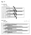
- a bistable circuit 140 shown in Fig. 10A is provided with a leading line 141 for supplying the clock signal from the main line, and an element 143 is provided at a position P1
- the bistable circuit 140 is configured such that the line 142 is provided between the bistable circuit 140 and an adjacently provided stage of the other shift register, and the clock signals are received using the line 142 (see Fig. 10B ) .
- Fig. 10C it is possible to reduce a layout area for the bistable circuit 140. Therefore, as shown in Fig.
- the width of the picture-frame area can be reduced by a length L in a direction in which the gate bus line extends.
- a gate driver having an equivalent function with the conventional example can be formed on a panel having a picture-frame area smaller than that in the conventional example.
- a contact for connecting the line 122 for the second clock CKB of the bistable circuit of the (4k-2) th stage with the line 113 for the third clock CKC of the bistable circuit of the (4k-3)th stage, and a contact for connecting the line 122 with the line 134 for the fourth clock CKD of the bistable circuit of the (4k-1) th stage are achieved by the single contact 125.
- each stage of the shift register 10 with a contact for supplying the clock signal received from the clock signal main line to both the preceding-side and succeeding-side stages of the other shift register, it is, possible to further reduce the picture-frame of the panel.
- a load capacitance accompanied by the clock signal main line can be reduced to, for example, about half of the conventional example.
- Fig. 12 is a schematic diagram illustrating the load capacitance accompanied by a single main line for every two of the bistable circuits in the gate driver 4 according to this embodiment.
- Fig. 13 is a schematic diagram illustrating the same contents shown in Fig. 12 for the conventional gate driver.
- the capacitance value C2 is 5fF, for example.
- the main lines are generally more than 10 times wider than the clock lines in the area of the shift register.
- the load capacitance according to this embodiment is reduced to about half of the conventional example. Therefore, it is possible to suppress mutual interference between the clock signals, and to reduce waveform rounding in the clock signals. Thus, as compared to the conventional example, it is possible to downsize the thin film transistors that constitute the shift register, thereby reducing the picture-frame area of the panel.
- each stage of the shift register 10 receives the clock signals that are not received from the clock signal main lines from the preceding or succeeding stage.
- the present invention is not limited to such an example.
- Each stage of the shift register may receive the clock signals that are not received from the clock signal main lines from a stage other than the preceding or succeeding stage of the shift register.
- each stage of the shift register may receive the first clock CKA supplied to the preceding stage as the fourth clock CKD, and the first clock CKA supplied to the succeeding stage as the third clock CKC.
- the bistable circuit 11 shown in Fig. 4 may include a capacitor, in place of the thin film transistor MF, between an input terminal for the third clock CKC and the second node N2.
- the gate driver 4 is disposed on one side of the display unit 7.
- gate drivers can be provided on both sides of the display unit 7. According to this configuration, it is possible to charge a single gate bus line from the both sides of the display unit 7, thereby eliminating a problem of insufficient charge of a large size panel.
- a thin film transistor whose drain electrode or source electrode is connected to the first node N1 may be configured as a multichannel TFT.
- a bistable circuit 12 shown in Fig. 15 is achieved by configuring the thin film transistors ML and ME as multichannel TFTs (ML2 and ME2) .
- bistable circuit 12 With the bistable circuit 12, it is possible to prevent a leakage current from flowing through the thin film transistors ML and ME and the potential of the first node N1 from decreasing.
- the use of multichannel TFTs is effective for a circuit using microcrystalline silicon having a relatively large off current.
- Fig. 16A is a plan view of the multichannel TFT
- Fig. 16B is a cross-sectional view taken along line A-A' in Fig. 16A
- Fig. 16C is an equivalent circuit diagram of the multichannel TFT.
- a multichannel TFT 150 shown in Figs. 16A and 16B has a dual-gate structure (double-gate structure), and electrically equivalent to two TFTs that are connected in series ( Fig. 16C ) .
- the multichannel TFT 150 is provided with an active layer 154 supported by a substrate 151 (glass substrate, for example) .
- the active layer 154 is a semiconductor layer and includes a microcrystalline silicon ( ⁇ c-Si) film.
- the active layer 154 is provided with channel regions 154c1 and 154c2 (hereinafter referred to as two channel regions), a source region 154s, a drain region 154d, and an intermediate region 154m formed between the two channel regions.
- the multichannel TFT 150 is further provided with a contact layer 156, an electrode layer 158, a gate electrode 152, and a protection film 159 that covers these components.
- the contact layer 156 includes a source contact region 156s in contact with the source region 154s, a drain contact region 156d in contact with the drain region 154d, and an intermediate contact region 156m in contact with the intermediate region 154m.
- the electrode layer 158 includes a source electrode 158s in contact with the source contact region 156s, a drain electrode 158d in contact with the drain contact region 156d, and an intermediate electrode 158m in contact with the intermediate contact region 156m.
- the gate electrode 152 faces toward the two channel regions and the intermediate region 154m with a gate insulation film 153 interposed therebetween.
- the intermediate electrode 158m is in a floating state.
- the channel region 154c1 is formed between the source region 154s and the intermediate region 154m, and the channel region 154c2 is formed between the drain region 154d and the intermediate region 154m.
- the two channel regions, the source region 154s, the drain region 154d, and the intermediate region 154m are formed into the single continuous active layer 154. Further, a part of the intermediate electrode 158m that is present between the two channel regions as a whole overlaps with the gate electrode 152, with the intermediate region 154m and the gate insulation film 153 interposed therebetween.
- the active layer 154 of the multichannel TFT 150 is formed by a microcrystalline silicon film, or a layered film of a microcrystalline silicon film and an amorphous silicon film, and can be manufactured using a manufacturing process for conventional amorphous silicon TFTs.
- the microcrystalline silicon film can be formed by, for example, employing a plasma CVD (Chemical Vapor Deposition) method similarly to the manufacturing method of the amorphous silicon film, using a silane gas diluted by a hydrogen gas as a material gas. It should be noted that the multichannel TFT can be applied to circuits using amorphous silicon or oxide semiconductor, and not limited to circuits using microcrystalline silicon.
- the liquid crystal display device according to second to fourth embodiments of the present invention is different from the liquid crystal display device according to the first embodiment in a configuration of a shift register included in a gate driver.
- the differences of the second to fourth embodiments from the first embodiment are described.
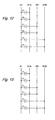
- Fig. 17 is a block diagram illustrating a gate driver according to the second embodiment of the present invention in detail.
- the gate driver according to this embodiment is provided with a shift register 20 including an odd-numbered stage shift register and an even-numbered stage shift register, and main lines including clock signal main lines.
- the dummy bistable circuits 21 and 22 do not include a thin film transistor as a switching device.
- the dummy bistable circuits 21 and 22 include, out of the components included in each stage of the shift register 20, only the components necessary to transmit the clock signal received from the clock signal main line.
- the dummy bistable circuit 21 is provided on a side of a first stage of the shift register 20.
- the third gate clock signal CK2 is supplied as the second clock CKB from the main line.
- the dummy bistable circuit 21 outputs the supplied second clock CKB without change.
- the second clock CKB outputted from the dummy bistable circuit 21 is supplied as the fourth clock CKD.
- the dummy bistable circuit 22 is provided on a side of a last stage of the shift register 20.
- the first gate clock signal CK1 (when a is an odd number) or the second gate clock signal CK1B (when a is an even number) is supplied as the second clock CKB from the main line.
- Fig. 17 shows a case where a is an odd number.
- the dummy bistable circuit 22 outputs the supplied second clock CKB without change.
- the second clock CKB outputted from the dummy bistable circuit 22 is supplied as the third clock CKC.
- each dummy bistable circuit is provided on each of the first and last stage sides of the shift register 20 in this example, a plurality of dummy bistable circuits can be provided on both of the first and last stage sides depending on the number of the clock signals necessary for the operation of the shift register.
- Fig. 18 is a schematic diagram illustrating a layout of the gate driver according to this embodiment.
- the dummy bistable circuits 21 and 22 include, out of the components included in each stage (the bistable circuit 11) of the shift register 20, only the components necessary to transmit the second clock CKB received from the clock signal main line.
- the dummy bistable circuit 21 is provided with a line 212 for the second clock CKB and a contact 215.
- the line 212 is connected to the main line for the third gate clock signal CK2 via a contact 217, and to a line 234 for the fourth clock CKD of the bistable circuit of the first stage via the contact 215 within the dummy bistable circuit 21.
- the dummy bistable circuit 22 is provided with a line 222 for the second clock CKB and a contact 225.
- the line 222 is connected to the main line for the first gate clock signal CK1 via a contact 227, and to a line 243 for the third clock CKC of the bistable circuit of the m-th stage via the contact 225 within the dummy bistable circuit 22.
- the layout of the gate driver according to this embodiment is the same as that of the first embodiment. In this embodiment, too, the leading lines from the clock signal main lines intersect with the clock lines for receiving the remaining part of the clock signals from the stage provided adjacently in the other shift register.
- the gate driver according to this embodiment is provided with the plurality of shift registers (the odd-numbered stage shift register and the even-numbered stage shift register), and the clock signal main lines.
- the plurality of shift registers include a shift register having the dummy bistable circuit 21 that supplies the second clock CKB received from the clock signal main line to the first stage without change (the odd-numbered stage shift register), and a shift register having the dummy bistable circuit 22 that supplies the second clock CKB received from the clock signal main line to the last stage without change (the even-numbered stage shift register).
- Fig. 19 is a block diagram illustrating a gate driver according to the third embodiment of the present invention in detail.
- the gate driver according to this embodiment is provided with a shift register 30 including an odd-numbered stage shift register and an even-numbered stage shift register, and main lines including clock signal main lines.
- Each bistable circuit 31 is configured such that a function of outputting a signal Z that changes in the same manner as the state signal Q is added to the bistable circuit 11 according to the first embodiment.
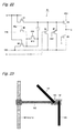
- Fig. 20 is a circuit diagram of the bistable circuit 31.
- the bistable circuit 31 is configured such that a thin film transistor MG is added to the bistable circuit 11.
- the thin film transistor MG outputs the first clock CKA as the signal Z while the potential of the first node N1 is at a high level.
- the state signal Q outputted from the bistable circuit 11 is used as the set signal S and the reset signal R.
- the signal Z generated by the thin film transistor MG is used as the set signal S and the reset signal R.
- the state signal Q is susceptible to waveform rounding.
- Using the state signal Q having waveform rounding as the set signal S and the reset signal R may possibly cause an error in the operation of the shift register.
- the signal Z generated separately from the state signal Q as the set signal S and the reset signal R it is possible to prevent an error in the operation of the shift register due to waveform rounding in the state signal Q.
- Fig. 21 is a block diagram illustrating a gate driver according to a reference example in detail.
- the gate driver shown in Fig. 21 is provided with a shift register 40 including an odd-numbered stage shift register and an even-numbered stage shift register, and main lines including clock signal main lines.
- Fig. 22 is a circuit diagram of the bistable circuit 41.
- the bistable circuit 41 operates based on two clock signals (the first clock CKA and the second clock CKB) .
- a signal delay easily occurs while the signal is transmitted from the first stage to the last stage of the shift register. Therefore, as shown in Fig. 21 , the shift registers whose odd-lumbered stage and even-numbered stage are different to each other can be provided. With this, focusing on a single shift register, the number of the stages in a shift register is reduced to half as compared to the conventional example.
- the gate driver shown in Fig. 21 similarly to the first to third embodiments, the number of clock signals supplied from the main lines to the bistable circuit ("1", in this case) is smaller than the number of clock signals necessary for operating a single bistable circuit ("2", in this case).
- the number of the leading lines from the main lines as well as intersecting portions between the leading lines and the clock main lines . This effectively prevents the signal from delaying.
- the contact for connecting the line (connected to the main line) for the second clock CKB of the bistable circuit of one stage with the line for the third clock CKC of the bistable circuit of the preceding stage, and the contact for connecting the line for the second clock CKB of this bistable circuit with the line for the fourth clock CKD of the bistable circuit of the succeeding stage are achieved by a single contact (see Fig. 8 ).
- the present invention is not limited to such an example. As shown in Fig.
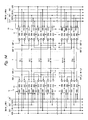
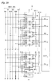
- Fig. 24 is a block diagram illustrating a gate driver according to the fourth embodiment of the present invention in detail.
- the gate driver according to this embodiment is provided with a shift register 50 including an odd-numbered stage shift register and an even-numbered stage shift register, and main lines including clock signal main lines.
- Each bistable circuit 51 is configured to have the same circuit configuration as that of the bistable circuit 11 according to the first embodiment (see Fig. 4 ). However, the bistable circuit 51 is different from the bistable circuit 11 in that the bistable circuit 51 outputs the inputted first clock CKA to neighboring stages (including an adjacent stage) as a clock signal for the neighboring stages (including the adjacent stage) in the shift register, while the bistable circuit 11 outputs the inputted second clock CKB to the neighboring stages (including the adjacent stage) as the clock signal for the neighboring stages (including the adjacent stage) in the shift register.
- the dummy bistable circuits 52 to 54 do not include a thin film transistor as a switching device, and includes, out of the components included in each stage (the bistable circuit 51) of the shift register 50, only the components necessary to transmit the clock signal received from the clock signal main line.
- the dummy bistable circuit 52 is provided on a side of a first stage of the shift register 20.
- the fourth gate clock signal CK2B is supplied as the first clock CKA from the main line.
- the dummy bistable circuits 53 and 54 are provided on a side of a last stage of the shift register 20.
- the second gate clock signal CK1B (when a is an odd number) or the first gate clock signal CK1 (when a is an even number) is supplied as the first clock CKA from the main line.
- the fourth gate clock signal CK2B (when a is an odd number) or the third gate clock signal CK2 (when a is an even number) is supplied as the first clock CKA from the main line.
- Fig. 24 shows a case where a is an odd number.
- the dummy bistable circuits 52 to 54 output the supplied first clock CKA without change.
- the signals supplied to each of the stages (the bistable circuits 51) of the shift register 50 are stated below.
- the low-potential direct-current voltage VSS and the clear signal CLR are supplied to all the stages in common.
- k is an integer not smaller than 1 and not greater than a predetermined integer
- the first gate clock signal CK1 is supplied as the first clock CKA.
- the third gate clock signal CK2 is supplied as the first clock CKA.
- the second gate clock signal CK1B is supplied as the first clock CKA.
- the fourth gate clock signal CK2B is supplied as the first clock CKA.
- Each stage of the shift register 10 receives the low-potential direct-current voltage VSS, the clear signal CLR, and the first clock CKA from the main lines.
- the first clock CKA outputted from the dummy bistable circuit 52 is supplied as the third clock CKC.
- the first clock CKA outputted from a preceding stage is supplied as the third clock CKC.
- the first clock CKA outputted from the dummy bistable circuit 53 is supplied as the fourth clock CKD.
- the first clock CKA outputted from a succeeding stage is supplied as the fourth clock CKD.
- the first clock CKA outputted from the dummy bistable circuit 54 is supplied as the second clock CKB.
- the first clock CKA outputted from the dummy bistable circuit 53 is supplied as the second clock CKB.
- the first clock CKA outputted from a second succeeding stage is supplied as the second clock CKB.
- Fig. 25 is a schematic diagram illustrating a layout of the gate driver according to this embodiment. To the four bistable circuits shown in Fig. 25 , it is necessary to supply the first clock CKA to be supplied to the thin film transistor MI, the second clock CKB for controlling the thin film transistor MD, the third clock CKC for controlling the thin film transistor MF, and the fourth clock CKD for controlling the thin film transistor MK.
- the bistable circuit of the (4k-2) th stage shown in Fig. 25 is provided with a line 521 for the first clock CKA, a line 522 for the second clock CKB, a line 523 for the third clock CKC, a line 524 for the fourth clock CKD, and contacts 525 and 526.
- the line 521 for the first clock CKA is connected to the main line for the third gate clock signal CK2 via a contact 527.
- the line 522 for the second clock CKB is connected to a line 541 for the first clock CKA of the bistable circuit of a 4k-th stage via a contact 546 provided for the bistable circuit of the 4k-th stage.
- the line 541 is connected to the main line for the fourth gate clock signal CK2B via a contact 547.
- the line 523 for the third clock CKC is connected to a line 511 for the first clock CKA of the bistable circuit of the (4k-3) th stage via a contact 515 provided for the bistable circuit of the (4k-3) th stage.
- the line 511 is connected to the main line for the first gate clock signal CK1 via a contact 517.
- the line 524 for the fourth clock CKD is connected to a line 531 for the first clock CKA of the bistable circuit of the (4k-1)th stage via a contact 535 provided for the bistable circuit of the (4k-1) th stage.
- the line 531 is connected to the main line for the second gate clock signal CK1B via a contact 537.
- the line 521 for the first clock CKA is connected to a line 533 for the third clock CKC of the bistable circuit of the (4k-1)th stage and to a line 514 for the fourth clock CKD of the bistable circuit of the (4k-3) th stage via a contact 525 within the bistable circuit of the (4k-2) th stage.
- the line 521 is connected to a line (not depicted) for the second clock CKB of the bistable circuit of a (4k-4)th stage via a contact 526 within the bistable circuit of the (4k-2)th stage.
- the other bistable circuits included in the shift register 50 are also laid out in a manner similar to that shown in Fig. 25 . As described above, each stage of the shift register 50 receives a part of the four clock signals from the clock signal main lines, a different part of the clock signals from the preceding or succeeding stage, and the remaining part of the clock signals from a second succeeding stage.
- the shift register 50 includes the odd-numbered stage shift register and the even-numbered stage shift register, where a stage preceding or succeeding to the odd-numbered stage is an even-numbered stage, and a stage preceding or succeeding to the even-numbered stage is an odd-numbered stage. Further, a second succeeding stage of the odd-numbered stage is an odd-numbered stage, and a second succeeding stage of the even-numbered stage is an even-numbered stage.
- each stage of the shift register 50 receives a part of the four clock signals from the clock signal main lines, a different part of the clock signals from the other shift register (more specifically, from a stage provided adjacently in the other shift register), and the remaining part of the clock signals from the same shift register (more specifically, from a succeeding stage of the same shift register).
- the line 531 for the first clock CKA of the bistable circuit of the (4k-1) th stage intersects with the line 533 for the third clock CKC of the bistable circuit of the (4k-1) th stage, and with the line 522 for the second clock CKB of the (4k-2)th stage.
- the leading lines from the clock signal main lines intersect with the clock lines for receiving the different part of the clock signals from the stage provided adjacently in the other shift register, and with the clock lines for receiving the remaining part of the clock signals from the succeeding stage of the same shift register.
- each stage of the shift register 50 receives the part of the clock signals from the clock signal main lines, the different part of the clock signals from the adjacently provided stage of the other shift register, and the remaining part of the clock signals from the succeeding stage of the same shift register. From a phase of the clock signal (the first clock CKA) supplied from the clock signal main line to the charge control switching device (the thin film transistor MI) , a phase of the different part of the clock signals (the third clock CKC and the fourth clock CKD) is displaced by 90 degrees, and a phase of the remaining part of the clock signals (second clock CKC) is displaced by 180 degrees.
- Each stage of the shift register 50 includes a contact (for example, the contact 525) for supplying the clock signal received from the clock signal main line to both the preceding-side and succeeding-side stages of the other shift register.
- each stage of the shift register 50 may include a contact (for example, the contact 525) for supplying the clock signal received from the clock signal main line to at least two of the preceding-side stage of the other shift register, the succeeding-side stage of the other shift register, and a different stage of the same shift register.
- each stage of the shift register 50 may separately include a contact for supplying the clock signal received from the clock signal main line to the preceding-side stage of the other shift register, a contact for supplying the same clock signal to the succeeding-side stage of the other shift register, and a contact for supplying the same clock signal to the different stage of the same shift register, and at least two of the three contacts are provided at adjacent positions so as to be in contact with each other, thereby electrically connecting the two adjacent contacts.
- each stage of the shift register 50 receives the remaining part of the clock signals from the succeeding stage of the same shift register, the remaining part of the clock signals may be received from the preceding stage of the same shift register.
- the present invention is not limited to such an example.
- the present invention can also be applied to a display device such as an organic EL (Electro Luminescence) display device, other than the liquid crystal display device.
- a scanning signal line drive circuit provides advantageous effects of reducing a layout area for shift registers, and of reducing a picture-frame area of a panel, and therefore can be applied to various display devices such as liquid crystal display devices and organic EL display devices.
Landscapes
- Engineering & Computer Science (AREA)
- Microelectronics & Electronic Packaging (AREA)
- Power Engineering (AREA)
- Chemical & Material Sciences (AREA)
- Crystallography & Structural Chemistry (AREA)
- Physics & Mathematics (AREA)
- Computer Hardware Design (AREA)
- General Physics & Mathematics (AREA)
- Theoretical Computer Science (AREA)
- Control Of Indicators Other Than Cathode Ray Tubes (AREA)
- Liquid Crystal Display Device Control (AREA)
- Liquid Crystal (AREA)
Applications Claiming Priority (3)
| Application Number | Priority Date | Filing Date | Title |
|---|---|---|---|
| JP2009166305 | 2009-07-15 | ||
| JP2009268410 | 2009-11-26 | ||
| PCT/JP2010/052329 WO2011007591A1 (ja) | 2009-07-15 | 2010-02-17 | 走査信号線駆動回路およびそれを備えた表示装置 |
Publications (2)
| Publication Number | Publication Date |
|---|---|
| EP2455931A1 true EP2455931A1 (de) | 2012-05-23 |
| EP2455931A4 EP2455931A4 (de) | 2013-05-15 |
Family
ID=43449201
Family Applications (1)
| Application Number | Title | Priority Date | Filing Date |
|---|---|---|---|
| EP10799655.5A Withdrawn EP2455931A4 (de) | 2009-07-15 | 2010-02-17 | Abtastsignal-anlagenantriebsschaltung und anzeigevorrichtung damit |
Country Status (7)
| Country | Link |
|---|---|
| US (1) | US8803784B2 (de) |
| EP (1) | EP2455931A4 (de) |
| JP (1) | JP5208277B2 (de) |
| CN (1) | CN102473385B (de) |
| BR (1) | BR112012000960A2 (de) |
| RU (1) | RU2491651C1 (de) |
| WO (1) | WO2011007591A1 (de) |
Cited By (2)
| Publication number | Priority date | Publication date | Assignee | Title |
|---|---|---|---|---|
| CN110010067A (zh) * | 2017-12-11 | 2019-07-12 | 乐金显示有限公司 | 栅极移位寄存器和包括其的有机发光显示设备 |
| EP3667651A4 (de) * | 2017-08-08 | 2021-01-27 | BOE Technology Group Co., Ltd. | Zeilentreiberschaltung und ansteuerungsverfahren dafür sowie anzeigevorrichtung |
Families Citing this family (28)
| Publication number | Priority date | Publication date | Assignee | Title |
|---|---|---|---|---|
| US8525567B2 (en) * | 2009-07-08 | 2013-09-03 | Nec Corporation | Pipeline circuit, semiconductor device, and pipeline control method |
| KR101349781B1 (ko) * | 2010-07-01 | 2014-01-09 | 엘지디스플레이 주식회사 | 게이트 구동부 및 이를 포함하는 액정표시장치 |
| US20150255171A1 (en) * | 2012-10-05 | 2015-09-10 | Sharp Kabushiki Kaisha | Display device |
| JP2014182203A (ja) * | 2013-03-18 | 2014-09-29 | Japan Display Inc | 表示装置および電子機器 |
| CN104575409B (zh) * | 2013-10-16 | 2017-08-18 | 瀚宇彩晶股份有限公司 | 液晶显示器及其双向移位暂存装置 |
| WO2016002644A1 (ja) * | 2014-07-04 | 2016-01-07 | シャープ株式会社 | シフトレジスタおよびそれを備える表示装置 |
| CN107004386B (zh) * | 2014-11-21 | 2019-10-15 | 夏普株式会社 | 显示装置 |
| CN105159507B (zh) * | 2015-10-22 | 2018-01-30 | 厦门天马微电子有限公司 | 阵列基板、触控显示装置及其驱动方法 |
| CN105405421B (zh) * | 2015-11-09 | 2018-04-20 | 深圳市华星光电技术有限公司 | 液晶显示设备及goa电路 |
| CN205282054U (zh) * | 2016-01-05 | 2016-06-01 | 北京京东方显示技术有限公司 | 一种移位寄存器单元、栅极驱动电路及显示面板 |
| CN105788529A (zh) * | 2016-05-10 | 2016-07-20 | 上海天马有机发光显示技术有限公司 | 一种有机发光显示面板及其驱动方法 |
| KR102526724B1 (ko) * | 2016-05-19 | 2023-05-02 | 삼성디스플레이 주식회사 | 표시 장치 |
| KR102569666B1 (ko) * | 2017-11-07 | 2023-08-22 | 엘지디스플레이 주식회사 | 표시장치 |
| CN106991979B (zh) * | 2017-05-25 | 2019-06-07 | 上海天马微电子有限公司 | 一种电子纸及显示装置 |
| CN107315291B (zh) * | 2017-07-19 | 2020-06-16 | 深圳市华星光电半导体显示技术有限公司 | 一种goa显示面板及goa显示装置 |
| CN107749276B (zh) * | 2017-11-28 | 2020-06-23 | 上海天马有机发光显示技术有限公司 | 一种有机发光显示面板及有机发光显示装置 |
| CN208141796U (zh) * | 2018-04-28 | 2018-11-23 | 京东方科技集团股份有限公司 | 移位寄存器单元、栅极驱动电路及显示装置 |
| CN109213380A (zh) * | 2018-11-12 | 2019-01-15 | 京东方科技集团股份有限公司 | 输入控制电路及方法、输入控制装置、显示面板 |
| CN110264937B (zh) * | 2019-06-27 | 2023-04-11 | 京东方科技集团股份有限公司 | 栅极驱动电路及其测试方法、和显示装置 |
| KR102729155B1 (ko) * | 2019-12-16 | 2024-11-14 | 삼성디스플레이 주식회사 | 표시 장치 및 이의 구동 방법 |
| CN111292696B (zh) * | 2020-02-27 | 2021-07-06 | 深圳市华星光电半导体显示技术有限公司 | Goa驱动电路及其goa阵列基板、显示面板、显示装置 |
| US11929030B2 (en) * | 2020-04-28 | 2024-03-12 | Chengdu Boe Optoelectronics Technology Co., Ltd. | Display panel, driving method, and display device |
| KR102788784B1 (ko) * | 2020-08-18 | 2025-04-01 | 삼성디스플레이 주식회사 | 게이트 구동부 및 이를 포함하는 표시 장치 |
| KR102813548B1 (ko) * | 2021-03-16 | 2025-05-28 | 삼성디스플레이 주식회사 | 표시 장치 및 이를 포함하는 타일형 표시 장치 |
| CN116312244B (zh) * | 2021-09-10 | 2025-06-06 | 厦门天马显示科技有限公司 | 显示面板及显示装置 |
| WO2023142043A1 (zh) * | 2022-01-29 | 2023-08-03 | 京东方科技集团股份有限公司 | 显示基板、显示装置、显示基板的制作方法 |
| CN117198180A (zh) * | 2022-05-31 | 2023-12-08 | 群创光电股份有限公司 | 一种电子装置 |
| CN114974164B (zh) * | 2022-08-02 | 2022-12-09 | 惠科股份有限公司 | 阵列基板和显示面板 |
Family Cites Families (44)
| Publication number | Priority date | Publication date | Assignee | Title |
|---|---|---|---|---|
| US4562435A (en) * | 1982-09-29 | 1985-12-31 | Texas Instruments Incorporated | Video display system using serial/parallel access memories |
| DE69027136T2 (de) * | 1989-02-10 | 1996-10-24 | Sharp Kk | Flüssigkristallanzeigeeinheit und Steuerverfahren dafür |
| US5136622A (en) * | 1991-02-28 | 1992-08-04 | Thomson, S.A. | Shift register, particularly for a liquid crystal display |
| US5410583A (en) * | 1993-10-28 | 1995-04-25 | Rca Thomson Licensing Corporation | Shift register useful as a select line scanner for a liquid crystal display |
| US5712653A (en) * | 1993-12-27 | 1998-01-27 | Sharp Kabushiki Kaisha | Image display scanning circuit with outputs from sequentially switched pulse signals |
| TW581906B (en) | 1995-10-14 | 2004-04-01 | Semiconductor Energy Lab | Display apparatus and method |
| CN100428319C (zh) | 2002-04-08 | 2008-10-22 | 三星电子株式会社 | 驱动电路及液晶显示器 |
| CN1666242A (zh) * | 2002-04-26 | 2005-09-07 | 东芝松下显示技术有限公司 | 用于场致发光显示屏的驱动电路 |
| AU2003241202A1 (en) | 2002-06-10 | 2003-12-22 | Samsung Electronics Co., Ltd. | Shift register, liquid crystal display device having the shift register and method of driving scan lines using the same |
| JP3896542B2 (ja) * | 2002-11-29 | 2007-03-22 | 日本テキサス・インスツルメンツ株式会社 | 走査駆動用集積回路 |
| JP3904524B2 (ja) * | 2003-03-20 | 2007-04-11 | シャープ株式会社 | 液晶表示装置およびその駆動方法 |
| JP3797366B2 (ja) * | 2004-03-29 | 2006-07-19 | セイコーエプソン株式会社 | 駆動回路、アクティブマトリクスパネル、及び表示パネル |
| KR101160822B1 (ko) * | 2004-07-27 | 2012-06-29 | 삼성전자주식회사 | 박막 트랜지스터 표시판 및 이를 포함하는 표시 장치 |
| TWI382264B (zh) * | 2004-07-27 | 2013-01-11 | Samsung Display Co Ltd | 薄膜電晶體陣列面板及包括此面板之顯示器裝置 |
| KR101056369B1 (ko) * | 2004-09-18 | 2011-08-11 | 삼성전자주식회사 | 구동유닛 및 이를 갖는 표시장치 |
| JP4714004B2 (ja) * | 2004-11-26 | 2011-06-29 | 三星モバイルディスプレイ株式會社 | 順次走査及び飛び越し走査兼用の駆動回路 |
| KR101191157B1 (ko) * | 2004-12-31 | 2012-10-15 | 엘지디스플레이 주식회사 | 액정표시장치의 구동부 |
| JP4899327B2 (ja) * | 2005-03-15 | 2012-03-21 | カシオ計算機株式会社 | シフトレジスタ回路及びその駆動制御方法並びに駆動制御装置 |
| KR101115730B1 (ko) * | 2005-03-31 | 2012-03-06 | 엘지디스플레이 주식회사 | 게이트 드라이버 및 이를 구비한 표시장치 |
| JP5154033B2 (ja) * | 2005-06-07 | 2013-02-27 | 三星電子株式会社 | 表示装置 |
| KR101166819B1 (ko) * | 2005-06-30 | 2012-07-19 | 엘지디스플레이 주식회사 | 쉬프트 레지스터 |
| US7267555B2 (en) * | 2005-10-18 | 2007-09-11 | Au Optronics Corporation | Electrical connectors between electronic devices |
| JP4654923B2 (ja) | 2006-01-26 | 2011-03-23 | カシオ計算機株式会社 | シフトレジスタ回路、及び表示駆動装置 |
| KR101256921B1 (ko) * | 2006-02-06 | 2013-04-25 | 삼성디스플레이 주식회사 | 게이트 구동유닛 및 이를 갖는 표시장치 |
| KR101404542B1 (ko) | 2006-05-25 | 2014-06-09 | 삼성디스플레이 주식회사 | 액정 표시 장치 |
| KR20080008795A (ko) | 2006-07-21 | 2008-01-24 | 삼성전자주식회사 | 표시 기판 및 이를 구비한 표시 장치 |
| JP4932415B2 (ja) * | 2006-09-29 | 2012-05-16 | 株式会社半導体エネルギー研究所 | 半導体装置 |
| US20080211760A1 (en) | 2006-12-11 | 2008-09-04 | Seung-Soo Baek | Liquid Crystal Display and Gate Driving Circuit Thereof |
| KR101329075B1 (ko) * | 2007-03-20 | 2013-11-12 | 엘지디스플레이 주식회사 | 액정표시장치 및 그의 구동 방법 |
| KR101307414B1 (ko) * | 2007-04-27 | 2013-09-12 | 삼성디스플레이 주식회사 | 게이트 구동 회로 및 이를 포함하는 액정 표시 장치 |
| US7633089B2 (en) | 2007-07-26 | 2009-12-15 | Semiconductor Energy Laboratory Co., Ltd. | Liquid crystal display device and electronic device provided with the same |
| KR101415562B1 (ko) * | 2007-08-06 | 2014-07-07 | 삼성디스플레이 주식회사 | 게이트 구동회로 및 이를 가지는 표시장치 |
| KR101437867B1 (ko) * | 2007-10-16 | 2014-09-12 | 삼성디스플레이 주식회사 | 표시 장치와 그 구동 장치 및 구동 방법 |
| US7831010B2 (en) * | 2007-11-12 | 2010-11-09 | Mitsubishi Electric Corporation | Shift register circuit |
| JP2009134814A (ja) * | 2007-11-30 | 2009-06-18 | Mitsubishi Electric Corp | シフトレジスタおよびそれを備える画像表示装置 |
| US8344989B2 (en) * | 2007-12-31 | 2013-01-01 | Lg Display Co., Ltd. | Shift register |
| TWI380274B (en) * | 2008-02-21 | 2012-12-21 | Chunghwa Picture Tubes Ltd | Shift register and liquid crystal display (lcd) |
| KR101286539B1 (ko) * | 2008-04-15 | 2013-07-17 | 엘지디스플레이 주식회사 | 쉬프트 레지스터 |
| TWI380275B (en) * | 2008-07-11 | 2012-12-21 | Wintek Corp | Shift register |
| KR101341005B1 (ko) * | 2008-12-19 | 2013-12-13 | 엘지디스플레이 주식회사 | 쉬프트 레지스터 |
| KR101022092B1 (ko) * | 2009-01-12 | 2011-03-17 | 삼성모바일디스플레이주식회사 | 쉬프트 레지스터 및 이를 이용한 유기전계발광 표시장치 |
| CN101847445B (zh) * | 2009-03-27 | 2012-11-21 | 北京京东方光电科技有限公司 | 移位寄存器及其栅线驱动装置 |
| JP5473408B2 (ja) * | 2009-05-29 | 2014-04-16 | 株式会社ジャパンディスプレイ | ゲート信号線駆動回路及び表示装置 |
| KR101350635B1 (ko) * | 2009-07-03 | 2014-01-10 | 엘지디스플레이 주식회사 | 듀얼 쉬프트 레지스터 |
-
2010
- 2010-02-17 US US13/379,556 patent/US8803784B2/en active Active
- 2010-02-17 RU RU2012105307/08A patent/RU2491651C1/ru not_active IP Right Cessation
- 2010-02-17 JP JP2011522747A patent/JP5208277B2/ja active Active
- 2010-02-17 EP EP10799655.5A patent/EP2455931A4/de not_active Withdrawn
- 2010-02-17 CN CN201080026629.3A patent/CN102473385B/zh active Active
- 2010-02-17 WO PCT/JP2010/052329 patent/WO2011007591A1/ja not_active Ceased
- 2010-02-17 BR BR112012000960A patent/BR112012000960A2/pt not_active IP Right Cessation
Cited By (3)
| Publication number | Priority date | Publication date | Assignee | Title |
|---|---|---|---|---|
| EP3667651A4 (de) * | 2017-08-08 | 2021-01-27 | BOE Technology Group Co., Ltd. | Zeilentreiberschaltung und ansteuerungsverfahren dafür sowie anzeigevorrichtung |
| CN110010067A (zh) * | 2017-12-11 | 2019-07-12 | 乐金显示有限公司 | 栅极移位寄存器和包括其的有机发光显示设备 |
| CN110010067B (zh) * | 2017-12-11 | 2022-04-15 | 乐金显示有限公司 | 栅极移位寄存器和包括其的有机发光显示设备 |
Also Published As
| Publication number | Publication date |
|---|---|
| US8803784B2 (en) | 2014-08-12 |
| JPWO2011007591A1 (ja) | 2012-12-20 |
| US20120105396A1 (en) | 2012-05-03 |
| JP5208277B2 (ja) | 2013-06-12 |
| CN102473385A (zh) | 2012-05-23 |
| WO2011007591A1 (ja) | 2011-01-20 |
| BR112012000960A2 (pt) | 2016-03-15 |
| RU2491651C1 (ru) | 2013-08-27 |
| EP2455931A4 (de) | 2013-05-15 |
| CN102473385B (zh) | 2014-11-26 |
Similar Documents
| Publication | Publication Date | Title |
|---|---|---|
| US8803784B2 (en) | Scanning signal line drive circuit and display device having the same | |
| KR101409110B1 (ko) | 표시 장치 | |
| US9001091B2 (en) | Scanning-signal-line driving circuit and display device including same | |
| EP2357642B1 (de) | Abtastsignalzeilen-ansteuerschaltung und schieberegister | |
| KR101245438B1 (ko) | 주사 신호선 구동 회로 및 그것을 구비한 표시 장치 | |
| EP2343710B1 (de) | Bidirektionales Schieberegister und Ansteuerungsverfahren dafür | |
| KR102007906B1 (ko) | 표시 패널 | |
| US20150145852A1 (en) | Display device | |
| US20130069930A1 (en) | Shift register, scanning signal line drive circuit, and display device | |
| US10777159B2 (en) | Gate driver and display apparatus having the same | |
| CN101952875A (zh) | 显示装置、显示装置的驱动方法、以及扫描信号线驱动电路 | |
| US20150255171A1 (en) | Display device | |
| US9842557B2 (en) | Gate driving circuit and display device having the same | |
| CN110658658B (zh) | 图像显示装置 | |
| US10473958B2 (en) | Shift register, display device provided with same, and method for driving shift register | |
| JP5536799B2 (ja) | シフトレジスタ及び表示装置 | |
| KR20170079509A (ko) | 액정표시장치 | |
| KR20140136254A (ko) | 스캔 구동부 및 이를 이용한 표시장치 | |
| US10360865B2 (en) | Gate driving circuit having high reliability and display device including the same | |
| US8665408B2 (en) | Liquid crystal display device | |
| KR20080040847A (ko) | 표시 장치 |
Legal Events
| Date | Code | Title | Description |
|---|---|---|---|
| PUAI | Public reference made under article 153(3) epc to a published international application that has entered the european phase |
Free format text: ORIGINAL CODE: 0009012 |
|
| 17P | Request for examination filed |
Effective date: 20120112 |
|
| AK | Designated contracting states |
Kind code of ref document: A1 Designated state(s): AT BE BG CH CY CZ DE DK EE ES FI FR GB GR HR HU IE IS IT LI LT LU LV MC MK MT NL NO PL PT RO SE SI SK SM TR |
|
| DAX | Request for extension of the european patent (deleted) | ||
| A4 | Supplementary search report drawn up and despatched |
Effective date: 20130416 |
|
| RIC1 | Information provided on ipc code assigned before grant |
Ipc: G09G 3/36 20060101AFI20130410BHEP Ipc: G02F 1/133 20060101ALI20130410BHEP Ipc: G09G 3/20 20060101ALI20130410BHEP |
|
| 17Q | First examination report despatched |
Effective date: 20140626 |
|
| STAA | Information on the status of an ep patent application or granted ep patent |
Free format text: STATUS: THE APPLICATION IS DEEMED TO BE WITHDRAWN |
|
| 18D | Application deemed to be withdrawn |
Effective date: 20170203 |