EP2455982A2 - Dünnschichtsolarzelle mit einer Polymerstreulichtschicht und Herstellungsverfahren dafür - Google Patents
Dünnschichtsolarzelle mit einer Polymerstreulichtschicht und Herstellungsverfahren dafür Download PDFInfo
- Publication number
- EP2455982A2 EP2455982A2 EP11189547A EP11189547A EP2455982A2 EP 2455982 A2 EP2455982 A2 EP 2455982A2 EP 11189547 A EP11189547 A EP 11189547A EP 11189547 A EP11189547 A EP 11189547A EP 2455982 A2 EP2455982 A2 EP 2455982A2
- Authority
- EP
- European Patent Office
- Prior art keywords
- light absorption
- layer
- polymer
- solar cell
- thin film
- Prior art date
- Legal status (The legal status is an assumption and is not a legal conclusion. Google has not performed a legal analysis and makes no representation as to the accuracy of the status listed.)
- Withdrawn
Links
Images


Classifications
-
- H—ELECTRICITY
- H10—SEMICONDUCTOR DEVICES; ELECTRIC SOLID-STATE DEVICES NOT OTHERWISE PROVIDED FOR
- H10F—INORGANIC SEMICONDUCTOR DEVICES SENSITIVE TO INFRARED RADIATION, LIGHT, ELECTROMAGNETIC RADIATION OF SHORTER WAVELENGTH OR CORPUSCULAR RADIATION
- H10F77/00—Constructional details of devices covered by this subclass
- H10F77/20—Electrodes
- H10F77/244—Electrodes made of transparent conductive layers, e.g. transparent conductive oxide [TCO] layers
-
- H—ELECTRICITY
- H10—SEMICONDUCTOR DEVICES; ELECTRIC SOLID-STATE DEVICES NOT OTHERWISE PROVIDED FOR
- H10F—INORGANIC SEMICONDUCTOR DEVICES SENSITIVE TO INFRARED RADIATION, LIGHT, ELECTROMAGNETIC RADIATION OF SHORTER WAVELENGTH OR CORPUSCULAR RADIATION
- H10F71/00—Manufacture or treatment of devices covered by this subclass
-
- H—ELECTRICITY
- H10—SEMICONDUCTOR DEVICES; ELECTRIC SOLID-STATE DEVICES NOT OTHERWISE PROVIDED FOR
- H10F—INORGANIC SEMICONDUCTOR DEVICES SENSITIVE TO INFRARED RADIATION, LIGHT, ELECTROMAGNETIC RADIATION OF SHORTER WAVELENGTH OR CORPUSCULAR RADIATION
- H10F77/00—Constructional details of devices covered by this subclass
- H10F77/10—Semiconductor bodies
- H10F77/16—Material structures, e.g. crystalline structures, film structures or crystal plane orientations
- H10F77/169—Thin semiconductor films on metallic or insulating substrates
- H10F77/1692—Thin semiconductor films on metallic or insulating substrates the films including only Group IV materials
-
- H—ELECTRICITY
- H10—SEMICONDUCTOR DEVICES; ELECTRIC SOLID-STATE DEVICES NOT OTHERWISE PROVIDED FOR
- H10F—INORGANIC SEMICONDUCTOR DEVICES SENSITIVE TO INFRARED RADIATION, LIGHT, ELECTROMAGNETIC RADIATION OF SHORTER WAVELENGTH OR CORPUSCULAR RADIATION
- H10F77/00—Constructional details of devices covered by this subclass
- H10F77/70—Surface textures, e.g. pyramid structures
- H10F77/707—Surface textures, e.g. pyramid structures of the substrates or of layers on substrates, e.g. textured ITO layer on a glass substrate
-
- Y—GENERAL TAGGING OF NEW TECHNOLOGICAL DEVELOPMENTS; GENERAL TAGGING OF CROSS-SECTIONAL TECHNOLOGIES SPANNING OVER SEVERAL SECTIONS OF THE IPC; TECHNICAL SUBJECTS COVERED BY FORMER USPC CROSS-REFERENCE ART COLLECTIONS [XRACs] AND DIGESTS
- Y02—TECHNOLOGIES OR APPLICATIONS FOR MITIGATION OR ADAPTATION AGAINST CLIMATE CHANGE
- Y02E—REDUCTION OF GREENHOUSE GAS [GHG] EMISSIONS, RELATED TO ENERGY GENERATION, TRANSMISSION OR DISTRIBUTION
- Y02E10/00—Energy generation through renewable energy sources
- Y02E10/50—Photovoltaic [PV] energy
Definitions
- Embodiments relate to a thin film solar cell and, more particularly, to a thin film solar cell with improved efficiency through increased light scattering coefficient and solar absorption thereof, and to a method for manufacturing the same.
- a solar cell is a device that converts light (solar energy) into electrical current (electrical energy) utilizing characteristics of semiconductors and has a PN junction structure formed by joining p-type and n-type semiconductors.
- solar energy solar energy
- electrical current electrical energy
- the solar cell may be classified into a bulk (substrate) solar cell and a thin film solar cell.
- the substrate solar cell is fabricated using a semiconductor material as a substrate, while the thin film solar cell is fabricated by forming a thin film semiconductor on a substrate, e.g., on a glass, or the like.
- the thin film solar cell may exhibit slightly reduced efficiency, as compared to the substrate solar cell, the thin film solar cell may be fabricated to a small thickness using a relatively low cost material. Therefore, the thin film solar cell may have reduced production costs and may be well suited for mass production.
- the thin film solar cell is generally manufactured by forming a front electrode on a substrate, e.g., on glass, providing a semiconductor light absorption layer on the front electrode, and forming a rear electrode above the light absorption layer. Light may be incident on the light absorption layer and converted to electrical energy.
- Some embodiments of the invention provide a thin film solar cell with a light scattering layer on a substrate to enhance light absorption by scattering long-wavelength solar radiation, as well as a method for manufacturing the same.
- Example embodiments provide a thin film solar cell, including a substrate, a light scattering layer on the substrate, a first electrode layer on the light scattering layer, a plurality of light absorption layers on the first electrode layer, and a second electrode layer on the plurality of light absorption layers.
- the light scattering layer may include a polymer.
- the light scattering layer may include a polymer doped with transparent conductive oxide nanoparticles.
- the transparent conductive oxide may be at least one of SnO 2 fluorine (F)-doped SnO 2 , aluminum (Al) and boron (B)-doped ZnO, ZrO 2 In 2 O 3 and TiO 2 .
- the polymer may include at least one of a UV-curable acrylate resin and a thermosetting acrylate resin.
- the light scattering layer may include a micropattern having an irregular arrangement of structures, the structures being pyramid-shaped or trapezoidal.
- the first electrode layer may include a transparent conductive oxide.
- the transparent conductive oxide may be at least one of SnO 2 , fluorine (F)-doped SnO 2 , aluminum (Al)-doped ZnO, boron (B)-doped ZnO, and TiO 2 .
- the plurality of light absorption layers may be sequentially stacked on each other, the plurality of light absorption layer including a first light absorption layer including amorphous silicon and a second light absorption layer including amorphous silicon-germanium and/or microcrystalline silicon.
- the plurality of light absorption layers may further include a third light absorption layer, the second light absorption layer including amorphous silicon-germanium, and the third light absorption layer including microcrystalline silicon.
- the plurality of light absorption layers may further include a third light absorption layer, the second light absorption layer including microcrystalline silicon, and a third light absorption layer including amorphous silicon-germanium.
- the second electrode layer may include a conductive material containing aluminum and silver.
- Example embodiments may also provide a method of manufacturing a thin film solar cell, including forming a light scattering layer a substrate, forming a first electrode layer on the light scattering layer, forming a plurality of light absorption layers on the first electrode layer, and forming a second electrode layer on the plurality of light absorption layers.
- the manufacturing method may further include applying a polymer to the substrate to form a polymer film, pressing a mold having a micropattern to the polymer film, hardening the polymer film while pressing the mold thereto, releasing the mold from the polymer film to form the light scattering layer, such that the micropattern is transformed from the mold to the polymer film, applying a transparent conductive oxide to the light scattering layer to form the first electrode layer, depositing a semiconductor material on the first electrode layer to form the plurality of light absorption layers, and applying a conductive material to the light absorption layers to form the second electrode layer.
- Applying the polymer to the substrate may include using a polymer including at least one of a UV-curable acrylate resin and a thermosetting acrylate resin. Imprinting a UV-curable acrylate resin or a thermosetting resin on a substrate to form a light scattering layer with irregularly arranged structures, may result that solar radiation of long wavelengths of more than about 800 nm is scattered from the light scattering layer.
- Applying the polymer to the substrate may further include doping the polymer with transparent conductive oxide nanoparticles.
- Using the doped polymer with the transparent conductive oxide may include using a polymer with at least one of SnO 2 fluorine (F)-doped SnO 2 aluminum (Al) and boron (B)-doped ZnO, ZrO 2 , In 2 O 3 and TiO 2 .
- Pressing the mold to the polymer film may include using a micropattern having a size ranging from about 800 nm to about 1200 nm.
- Hardening the polymer may include curing the polymer using heat or UV radiation.
- Forming the first electrode layer may include applying the transparent conductive oxide to the light scattering layer through sputtering or LPCVD. Applying the transparent conductive oxide to the light scattering layer to form the first electrode layer with irregularly arranged structures by sputtering or LPCVD may result that solar radiation of short wavelengths ranging from about 200 nm to about 800 nm is scattered from the first electrode layer;
- Applying the transparent conductive oxide may include using at least one of SnO 2 , fluorine (F)-doped SnO 2 , aluminum (Al)-doped ZnO, boron (B)-doped ZnO, and TiO 2 .
- Forming the plurality of light absorption layers may include depositing amorphous silicon on the first electrode layer to form a first light absorption layer, and depositing at least one of amorphous silicon-germanium and microcrystalline silicon on the first light absorption layer to form a second light absorption layer.
- a method for manufacturing a thin film solar cell including imprinting a UV-curable acrylate resin or a thermosetting resin on a substrate to form a light scattering layer with irregularly arranged structures, such that solar radiation of long wavelengths of more than about 800 nm is scattered from the light scattering layer, applying transparent conductive oxide to the light scattering layer to form a first electrode layer with irregularly arranged structures by sputtering or LPCVD, such that solar radiation of short wavelengths ranging from about 200 nm to about 800 nm is scattered from the first electrode layer, depositing a semiconductor material on the first electrode layer to form a plurality of light absorption layers, and applying a conductive material on light absorption layers to form a second electrode layer.
- FIGS. 1A, 1B , 1C and 1D illustrate schematic views of cross-sections of a thin film solar cell according to embodiments
- FIG. 2 illustrates a scanning electron microscope (SEM) image of a micropattern of a light scattering layer according to an embodiment
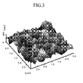
- FIG. 3 illustrates an atomic force microscope (AFM) image of a micropattern of a light scattering layer according to an embodiment
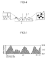
- FIG. 4 illustrates a conceptual view of a scattered condition of solar radiation from a light scattering layer according to an embodiment
- FIG. 5 illustrates a graph showing results of measuring the cross-section of the light scattering layer according to an embodiment through AFM
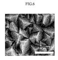
- FIG. 6 illustrates an SEM image of a micropattern of a first electrode layer according to an embodiment
- FIG. 7 illustrates conceptual views of processes in a method for manufacturing a thin film solar cell according to an embodiment.
- FIGS. 1A and 1B are schematic views of cross-sections of a thin film solar cell according to an embodiment.
- a thin film solar cell may include a substrate 1, a light scattering layer 2 provided on a front side, i.e., top surface, of the substrate 1, a first electrode layer 4 provided on a front side of the light scattering layer 2, and a light absorption layer 5 provided on a front side of the first electrode layer 4.
- the light scattering layer 2 may be between the substrate 1 and the first electrode layer 4.
- the substrate 1 may be prepared using a transparent glass substrate or a plastic substrate.
- the substrate 1 may include one or more of polyethylene terephthalate (PET), polyethylene naphthalate (PEN), polyether sulfone (PES), polyimide (PI), or the like.
- PET polyethylene terephthalate
- PEN polyethylene naphthalate
- PES polyether sulfone
- PI polyimide
- the substrate 1 may be rigid or flexible.
- the light scattering layer 2 may be formed on, e.g., directly on, the substrate 1.
- the light scattering layer 2 may be prepared using a polymer, and may be formed on a top surface of the substrate 1 through nano-imprint lithography.
- the polymer used for the light scattering layer 2 may be a UV-curable acrylate resin or a thermosetting acrylate resin.
- the light scattering layer 2 may include a micropattern formed therein, as will be described in more detail with reference to FIGS. 2-3 .
- FIG. 2 is a SEM image illustrating a micropattern of the light scattering layer 2
- FIG. 3 is an AFM image illustrating a micropattern of the light scattering layer 2.
- the light scattering layer 2 may have a micropattern formed by imprinting.
- the micropattern may have an irregular arrangement of structures, e.g., pyramid-shaped embossments or trapezoidal embossments. That is, marks, e.g., polygonal-shaped marks, may be pressed into a top surface 2a, i.e., a surface facing away from the substrate 1, of the light scattering layer 2 in an irregular arrangement, such that the top surface 2a of the light scattering layer 2 may include an arrangement of depressions and protrusions to define a rough, i.e., uneven, surface.
- the structures of the micropattern may have irregular shapes and/or an irregular arrangement on the top surface 2a of the light scattering film 2.
- the micropattern of the light scattering layer 2 may efficiently scatter solar radiation incident through the substrate 1, as illustrated in FIG. 4 (enlarged part A).
- the micropattern of the light scattering layer 2 may efficiently scatter long-wavelength solar radiation, i,e., light having a wavelength of about 800 nm or higher.
- the micropattern of the light scattering layer 2 may have a lateral feature size ranging from about 800 nm to about 1200 nm and a surface roughness ranging from about 100 nm to about 300 nm (see FIG. 5 ).
- the nano-imprint lithography (NIL) process is performed by applying a thermosetting resin or a UV-curable resin to a substrate, and hardening the same while pressing a mold, on which nano-sized micropattern is present, to the coated resin on the substrate. As such, the micropattern of the mold is transferred onto the resin coated on the substrate.
- the imprint resin may be applied to the substrate through spin-coating, slit-coating, dispensing, or the like.
- a light scattering layer 2' may be formed of a polymer doped with transparent conductive oxide (TCO) nanoparticles 3.
- TCO transparent conductive oxide
- the nanoparticles 3 may have a size of about 20 nm to about 500 nm.
- TCO may include SnO 2 , fluorine (F)-doped SnO 2 , aluminum (A1) and boron (B)-doped ZnO, ZrO 2 , In 2 O 3 , TiO 2 , or mixtures thereof.
- the light scattering layer 2' formed of a polymer, e.g., a UV-curable acrylate resin or a thermosetting acrylate resin, doped with the TCO nanoparticles 3 may efficiently scatter the solar radiation by the TCO nanoparticles 3 contained in the polymer, as illustrated in FIG. 4 (enlarged part B). If the light scattering film 2' includes both the micropattern and the TCO nanoparticles 3, scattering efficiency may be increased further.
- the polymer used for the light scattering layer 2 may have a refractive index ranging from about 1.5 to about 1.7 in relation to the solar radiation with a wavelength of about 587 nm.
- the doped polymer used for the light scattering layer 2' may have a refractive index ranging from about 1.5 to about 1.9 in relation to the solar radiation with a wavelength of about 587 nm, and the TCO nanoparticles 3 may have a refractive index of about 1.5 to about 2.5 in relation to the solar radiation with a wavelength of about 587 nm.
- the first electrode layer 4 may be formed on the light scattering layer 2 using TCO.
- TCO may include SnO 2 , fluorine (F)-doped SnO 2 , aluminum (Al)-doped ZnO, boron (B)-doped ZnO, TiO 2 , or mixtures thereof.
- the first electrode layer 4 may be provided on the light scattering layer 2 (or light scattering layer 2') through sputtering or LPCVD.
- the first electrode layer 4 may have a micropattern including an irregular arrangement of structures, e.g., pyramid-shaped embossments or trapezoidal embossments ( FIG. 6 ).
- the first electrode layer 4 may have a refractive index ranging from about 1.8 to about 2.5 in relation to solar radiation with a wavelength of about 587 nm.
- a lateral feature size of the micropattern in the first electrode layer 4 may range from about 50 nm to about 800 nm, while a surface roughness of the same may range from about 10 nm to about 100 nm ( FIG. 6 ).
- the first electrode layer 4 may efficiently scatter short-wavelength solar radiation, e.g., wavelengths at about 200 to about 800 nm.
- a thin film solar cell may include a double-textured structure for the light scattering layer 2 and the first electrode layer 4. That is, each of the light scattering layer 2 and the first electrode layer 4 may have a micropattern of irregularly arranged structures.
- the micropattern of the light scattering layer 2 may be different from the micropattern of the first electrode layer 4 in terms of surface roughness and lateral feature size in order to adjust scattering of different wavelengths, i.e., long vs. short wavelengths.
- the thin film solar cell may efficiently scatter long-wavelength solar radiation, i.e., at about 800 nm or higher, via the light scattering layer 2 and short-wavelength solar radiation, e.g., at about 200 nm to about 800 nm, via the first electrode layer 4.
- An optical path of solar radiation in the thin film solar cell according to example embodiments may be increased and solar absorption onto the light absorption layer 5 may also be increased. As such the solar cell efficiency may be improved further.
- the light absorption layer 5 may be formed using a semiconductor material, e.g., silicon, and may be provided on a front side of the first electrode layer 4. More particularly, the light absorption layer 5 may have a PIN structure including a positive (P-type) semiconductor layer, an intrinsic (I-type) semiconductor layer, and a negative (N-type) semiconductor layer. The light absorption layer 5 may be a single layer or a multi-layer structure.
- solar radiation incident upon the light absorption layer 5 through a substrate 1 penetrates a p-type amorphous silicon layer, is absorbed into an I-type amorphous silicon layer, and generates electrons and holes in the I-type amorphous silicon layer by solar radiation that has greater energy than an optical band gap of amorphous silicon within the I-type amorphous silicon layer.
- Such electrons and holes generated in the I-type amorphous silicon layer are collected in an N-type amorphous silicon layer as well as the P-type amorphous silicon layer, respectively, by an internal electric field, and then, are supplied to an external circuit, via electrodes such as the first electrode layer 4 and a second electrode layer.
- the light absorption layer 5 may have a multi-layer structure, i.e., the light absorption layer 5 may include a plurality of light absorption layers stacked on top of each other.
- the light absorption layer 5 may include a first light absorption layer 51 and a second light absorption layer 52 provided on a front side of the first absorption layer 51.
- the first light absorption layer 51 may have a PIN structure including amorphous silicon (a-Si)
- the second light absorption layer 52 may have a PIN structure including amorphous silicon-germanium (a-Si:Ge) or microcrystalline silicon ( ⁇ c-Si).
- the light absorption layer 5 may include a first light absorption layer 51, a second light absorption layer 52 provided on a front side of the first light absorption layer 51, and a third light absorption layer 53provided on a front side of the second light absorption layer 52.
- the first light absorption layer 51 may have a PIN structure including amorphous silicon (a-Si)
- the second light absorption layer 52 may have a PIN structure including amorphous silicon-germanium (a-Si:Ge)
- the third light absorption layer 53 may have a PIN structure including microcrystalline silicon ( ⁇ c-Si).
- the second light absorption layer 52 may have a PIN structure including microcrystalline silicon ( ⁇ c-Si), and the third light absorption layer 53 may have a PIN structure including amorphous silicon-germanium (a-Si:Ge).
- ⁇ c-Si microcrystalline silicon
- a-Si:Ge amorphous silicon-germanium
- the first light absorption layer 51 may absorb short-wavelength solar radiation, e.g., at about 200 nm to about 800 nm, while the second and/or third light absorption layers 52, 53 may absorb long-wavelength solar radiation, e.g., at more than 800 nm.
- the long-wavelength solar radiation i.e., light having a wavelength of more than 800 nm
- the short-wavelength solar radiation i.e., light having a wavelength ranging from about 200 nm to about 800 nm
- the first electrode layer 4 is scattered through the first electrode layer 4 and is absorbed in the first light absorption layer 51. Therefore, both the long-wavelength solar radiation and the short-wavelength solar radiation are uniformly absorbed, thereby improving solar cell efficiency.
- the second electrode layer 7 may be provided on a front side of the light absorption layer 5, and may be prepared using a conductive material containing aluminum (Al) and/or silver (Ag) which have excellent solar reflectance.
- FIG. 7 is a schematic view illustrating processes of a manufacturing method of a thin film solar cell according to an embodiment. The stages in the manufacturing process are designed by (a) through (f) in FIG. 7 .
- a polymer 2" used for imprinting is applied to the substrate 1 (part (a) of FIG. 7 ).
- the polymer 2" may be UV-curable acrylate resin or a thermosetting acrylate resin.
- the polymer 2" may be doped with TCO nanoparticles 3, e.g., particles of SnO 2 , fluorine (F)-doped SnO 2 , aluminum (Al) and boron (B)-doped ZnO, ZrO 2 , In 2 O 3 , TiO 2 or mixtures thereof.
- the polymer 2" may be applied to the substrate 1 through spin-coating, slit-coating and/or dispensing.
- a mold 6 may be pressed to the polymer 2" (part (b) of FIG. 7 ).
- the mold 6 may include a micropattern structure imprinted thereon, i.e., a micropattern having irregularly arranged positive and negative parts. Such a micropattern may have an irregular arrangement of pyramid-shaped or trapezoidal embosses.
- the pressing of the mold may be conducted using a roller under a pressure of about 0.8 MPa while operating the roller at a speed of about 0.05 m/s.
- a surface of the mold may be subjected to anti-adhesive coating before the imprinting process.
- UV irradiation After pressing the mold 6 to the polymer, heating or UV irradiation may be conducted to harden the polymer 2" into the light scattering layer 2 (part (c) of FIG. 7 ).
- the mold 6 In the case of UV irradiation, the mold 6 may be made of UV permeable materials.
- the UV radiation curing may be executed for about 30 seconds to about 90 seconds using a UV lamp that has a wavelength of about 365 nm and an intensity of about 2.3 mW/cm 2 as a light source.
- the mold 6 After hardening the polymer 2", the mold 6 is released from the polymer of the substrate 1.
- negative parts i.e., corresponding to positive parts of the mold 6
- positive parts i.e., corresponding to negative parts of the mold
- the micropattern may have a lateral feature size ranging from about 800 nm to about 1200 nm and a surface roughness ranging from about 100 nm to about 300 nm.
- TCO may be applied to a front side of the light scattering layer 2.
- the TCO may include SnO 2 , fluorine (F)-doped SnO 2 , aluminum (Al)-doped ZnO, boron (B)-doped ZnO, TiO 2 or mixtures thereof.
- the TCO may be deposited on the front side of the light scattering layer 2 through sputtering or LPCVD, in order to form the first electrode layer 4 (part (e) of FIG. 7 ).
- a double-texture type structure, as described above, may scatter both the long-wavelength solar radiation and the short-wavelength solar radiation, thereby increasing an optical path length (OPL) and enhancing the efficiency of a solar cell.
- OPL optical path length
- the light absorption layer 5 may be provided on top of the first electrode layer 4 (part (f) of FIG. 7 ).
- the light absorption layer 5 may be formed using any semiconductor material such as amorphous silicon, amorphous silicon-germanium, microcrystalline silicon, or the like, and have a multiple and/or tandem structure.
- a first light absorption layer 51 and a second light absorption layer 52, as described above, may be sequentially laminated on the first electrode layer 4.
- a third light absorption layer 53 may be further provided on the second light absorption layer 52.
- These light absorption layers may be sequentially formed above the first electrode layer 4 by any conventional deposition method such as CVD.
- a second electrode layer 7 made of a conductive material having a high light reflectance such as aluminum, silver, or the like, may be provided on a front side of the light absorption layer 5.
- a light scattering coefficient of the long-wavelength solar radiation is improved to preferably increase an optical path length (OPL), thus enhancing efficiency of the solar cell.
- OPL optical path length
- the efficiency of the solar cell may be further improved.
- a conventional thin film solar cell may transmit short-wavelength solar radiation through a light absorption layer formed of a transparent conductive film on a front electrode
- the conventional thin film solar cell may exhibit a low scattering coefficient with respect to long-wavelength solar radiation. As such, the conventional thin film solar cell may have poor absorption of long-wavelength solar radiation.
- Example embodiments have been disclosed herein, and although specific terms are employed, they are used and are to be interpreted in a generic and descriptive sense only and not for purpose of limitation. In some instances, as would be apparent to one of ordinary skill in the art as of the filing of the present application, features, characteristics, and/or elements described in connection with a particular embodiment may be used singly or in combination with features, characteristics, and/or elements described in connection with other embodiments unless otherwise specifically indicated. Accordingly, it will be understood by those of skill in the art that various changes in form and details may be made without departing from the scope of the example embodiments as set forth in the following claims.
Landscapes
- Photovoltaic Devices (AREA)
Applications Claiming Priority (1)
| Application Number | Priority Date | Filing Date | Title |
|---|---|---|---|
| KR1020100114652A KR20120053403A (ko) | 2010-11-17 | 2010-11-17 | 박막형 태양전지 및 그 제조방법 |
Publications (2)
| Publication Number | Publication Date |
|---|---|
| EP2455982A2 true EP2455982A2 (de) | 2012-05-23 |
| EP2455982A3 EP2455982A3 (de) | 2012-11-07 |
Family
ID=45002745
Family Applications (1)
| Application Number | Title | Priority Date | Filing Date |
|---|---|---|---|
| EP11189547A Withdrawn EP2455982A3 (de) | 2010-11-17 | 2011-11-17 | Dünnschichtsolarzelle mit einer Polymerstreulichtschicht und Herstellungsverfahren dafür |
Country Status (3)
| Country | Link |
|---|---|
| US (1) | US20120118365A1 (de) |
| EP (1) | EP2455982A3 (de) |
| KR (1) | KR20120053403A (de) |
Families Citing this family (7)
| Publication number | Priority date | Publication date | Assignee | Title |
|---|---|---|---|---|
| KR101511406B1 (ko) * | 2011-05-04 | 2015-04-10 | 한양대학교 산학협력단 | 비추적식 집광형 태양전지 모듈 |
| US20140004648A1 (en) * | 2012-06-28 | 2014-01-02 | International Business Machines Corporation | Transparent conductive electrode for three dimensional photovoltaic device |
| KR101632632B1 (ko) * | 2014-10-22 | 2016-06-22 | 주식회사 포스코 | 투명 전극 및 이를 구비하는 태양전지 |
| KR102471737B1 (ko) * | 2015-05-08 | 2022-11-28 | 고려대학교 산학협력단 | 패턴 구조물 및 패턴 구조물의 제조 방법 |
| KR102471349B1 (ko) * | 2015-05-08 | 2022-11-29 | 고려대학교 산학협력단 | 패턴 구조물의 제조 방법 |
| EP3147954A1 (de) | 2015-09-22 | 2017-03-29 | Nokia Technologies Oy | Fotodetektor mit leitfähigem kanal aus einem zweidimensionalen material und dessen herstellungsverfahren |
| EP4107790A4 (de) * | 2020-02-18 | 2024-03-13 | Gaf Energy LLC | Fotovoltaisches modul mit texturiertem superstrat mit schindelartigem aussehen |
Family Cites Families (12)
| Publication number | Priority date | Publication date | Assignee | Title |
|---|---|---|---|---|
| CN1093985C (zh) * | 1996-05-17 | 2002-11-06 | 佳能株式会社 | 光电元件的制造方法 |
| EP0827213A3 (de) * | 1996-08-28 | 1999-05-19 | Canon Kabushiki Kaisha | Photovoltaische Vorrichtung |
| JPH11191632A (ja) * | 1997-10-21 | 1999-07-13 | Sharp Corp | 薄膜太陽電池およびその製造方法 |
| EP0911884B1 (de) * | 1997-10-27 | 2005-02-09 | Sharp Kabushiki Kaisha | Photoelektrische Wandler und sein Herstellungsverfahren |
| JP3749015B2 (ja) * | 1998-03-23 | 2006-02-22 | シャープ株式会社 | 太陽電池の製造方法 |
| US6077722A (en) * | 1998-07-14 | 2000-06-20 | Bp Solarex | Producing thin film photovoltaic modules with high integrity interconnects and dual layer contacts |
| JP4811628B2 (ja) * | 2003-09-05 | 2011-11-09 | 日立化成工業株式会社 | 集光フィルム及び太陽電池ユニット |
| FR2915834B1 (fr) * | 2007-05-04 | 2009-12-18 | Saint Gobain | Substrat transparent muni d'une couche electrode perfectionnee |
| KR20100006226A (ko) * | 2008-07-09 | 2010-01-19 | 엘지디스플레이 주식회사 | 박막 태양전지 및 그 제조방법 |
| WO2010027253A2 (en) * | 2008-09-03 | 2010-03-11 | Moser Baer Photo Voltaic Ltd. | Method for producing a light trapping layer on a transparent substrate for use in a photovoltaic device, a method for producing a photovoltaic device as well as such a photovoltaic device |
| EP2328184A1 (de) * | 2008-09-12 | 2011-06-01 | Ulvac, Inc. | Solarzelle und verfahren zur herstellung der solarzelle |
| DE102009006719A1 (de) * | 2009-01-29 | 2010-08-12 | Schott Ag | Dünnschichtsolarzelle |
-
2010
- 2010-11-17 KR KR1020100114652A patent/KR20120053403A/ko not_active Withdrawn
-
2011
- 2011-11-15 US US13/296,333 patent/US20120118365A1/en not_active Abandoned
- 2011-11-17 EP EP11189547A patent/EP2455982A3/de not_active Withdrawn
Non-Patent Citations (1)
| Title |
|---|
| None |
Also Published As
| Publication number | Publication date |
|---|---|
| US20120118365A1 (en) | 2012-05-17 |
| KR20120053403A (ko) | 2012-05-25 |
| EP2455982A3 (de) | 2012-11-07 |
Similar Documents
| Publication | Publication Date | Title |
|---|---|---|
| US20120183690A1 (en) | Method of imprinting texture on rigid substrate using flexible stamp | |
| EP2455982A2 (de) | Dünnschichtsolarzelle mit einer Polymerstreulichtschicht und Herstellungsverfahren dafür | |
| Lin et al. | Efficient light absorption with integrated nanopillar/nanowell arrays for three-dimensional thin-film photovoltaic applications | |
| Yun et al. | Incident light adjustable solar cell by periodic nanolens architecture | |
| Mendes et al. | Optimal-enhanced solar cell ultra-thinning with broadband nanophotonic light capture | |
| US20120240999A1 (en) | Photoelectric conversion device and method of manufacturing photoelectric conversion device | |
| CN102934234B (zh) | 使用增强的光捕获方案的薄膜光伏器件 | |
| US20110186119A1 (en) | Light-trapping plasmonic back reflector design for solar cells | |
| EP2153474A1 (de) | Fotovoltageanordnung mit verbessertem lichtgewinn | |
| Wang et al. | Large-scale bio-inspired flexible antireflective film with scale-insensitivity arrays | |
| CN101866989A (zh) | 薄膜光伏器件 | |
| CN103474576A (zh) | 一种有机太阳能电池及其制作方法 | |
| Paetzold et al. | Thin-film silicon solar cell development on imprint-textured glass substrates | |
| KR102574926B1 (ko) | 페로브스카이트 실리콘 탠덤 태양전지 및 이의 제조 방법 | |
| CN102468442A (zh) | 光电转换元件以及光电转换元件的制造方法 | |
| US11581150B2 (en) | Perovskite silicon tandem solar cell and method for manufacturing the same | |
| Chen et al. | Enhanced performance of organic thin film solar cells using electrodes with nanoimprinted light-diffraction and light-diffusion structures | |
| EP2645442A2 (de) | Mehrere Lichtverwaltungstexturen | |
| KR101294835B1 (ko) | 양자점 태양전지 및 그 제조방법 | |
| Dong et al. | Flexible a‐Si: H Solar Cells with Spontaneously Formed Parabolic Nanostructures on a Hexagonal‐Pyramid Reflector | |
| KR101018319B1 (ko) | 유무기 복합 적층형 태양전지의 제조방법 | |
| JP5332088B2 (ja) | 光電変換素子およびその製造方法 | |
| KR101406882B1 (ko) | 텍스쳐링 표면을 가진 투명 필름을 이용한 유기 박막 태양전지 | |
| US20120167938A1 (en) | Solar cell, solar cell system, and method for making the same | |
| US20130295713A1 (en) | Modification and Optimization of a Light Management Area |
Legal Events
| Date | Code | Title | Description |
|---|---|---|---|
| PUAI | Public reference made under article 153(3) epc to a published international application that has entered the european phase |
Free format text: ORIGINAL CODE: 0009012 |
|
| AK | Designated contracting states |
Kind code of ref document: A2 Designated state(s): AL AT BE BG CH CY CZ DE DK EE ES FI FR GB GR HR HU IE IS IT LI LT LU LV MC MK MT NL NO PL PT RO RS SE SI SK SM TR |
|
| AX | Request for extension of the european patent |
Extension state: BA ME |
|
| RAP1 | Party data changed (applicant data changed or rights of an application transferred) |
Owner name: SAMSUNG ELECTRONICS CO., LTD. Owner name: SAMSUNG SDI CO., LTD. |
|
| PUAL | Search report despatched |
Free format text: ORIGINAL CODE: 0009013 |
|
| AK | Designated contracting states |
Kind code of ref document: A3 Designated state(s): AL AT BE BG CH CY CZ DE DK EE ES FI FR GB GR HR HU IE IS IT LI LT LU LV MC MK MT NL NO PL PT RO RS SE SI SK SM TR |
|
| AX | Request for extension of the european patent |
Extension state: BA ME |
|
| RIC1 | Information provided on ipc code assigned before grant |
Ipc: H01L 31/0236 20060101ALI20120928BHEP Ipc: H01L 31/052 20060101AFI20120928BHEP Ipc: H01L 31/18 20060101ALI20120928BHEP |
|
| STAA | Information on the status of an ep patent application or granted ep patent |
Free format text: STATUS: THE APPLICATION IS DEEMED TO BE WITHDRAWN |
|
| 18D | Application deemed to be withdrawn |
Effective date: 20130508 |