EP2458630A2 - Conditionnement et structure de terminal haute fréquence pour celui-ci - Google Patents
Conditionnement et structure de terminal haute fréquence pour celui-ci Download PDFInfo
- Publication number
- EP2458630A2 EP2458630A2 EP20110170561 EP11170561A EP2458630A2 EP 2458630 A2 EP2458630 A2 EP 2458630A2 EP 20110170561 EP20110170561 EP 20110170561 EP 11170561 A EP11170561 A EP 11170561A EP 2458630 A2 EP2458630 A2 EP 2458630A2
- Authority
- EP
- European Patent Office
- Prior art keywords
- disposed
- metal wall
- lower layer
- layer feed
- package according
- Prior art date
- Legal status (The legal status is an assumption and is not a legal conclusion. Google has not performed a legal analysis and makes no representation as to the accuracy of the status listed.)
- Granted
Links
Images






Classifications
-
- H—ELECTRICITY
- H10—SEMICONDUCTOR DEVICES; ELECTRIC SOLID-STATE DEVICES NOT OTHERWISE PROVIDED FOR
- H10W—GENERIC PACKAGES, INTERCONNECTIONS, CONNECTORS OR OTHER CONSTRUCTIONAL DETAILS OF DEVICES COVERED BY CLASS H10
- H10W76/00—Containers; Fillings or auxiliary members therefor; Seals
- H10W76/10—Containers or parts thereof
- H10W76/12—Containers or parts thereof characterised by their shape
- H10W76/13—Containers comprising a conductive base serving as an interconnection
- H10W76/134—Containers comprising a conductive base serving as an interconnection having other interconnections parallel to the conductive base
-
- H—ELECTRICITY
- H10—SEMICONDUCTOR DEVICES; ELECTRIC SOLID-STATE DEVICES NOT OTHERWISE PROVIDED FOR
- H10D—INORGANIC ELECTRIC SEMICONDUCTOR DEVICES
- H10D30/00—Field-effect transistors [FET]
- H10D30/40—FETs having zero-dimensional [0D], one-dimensional [1D] or two-dimensional [2D] charge carrier gas channels
- H10D30/47—FETs having zero-dimensional [0D], one-dimensional [1D] or two-dimensional [2D] charge carrier gas channels having two-dimensional [2D] charge carrier gas channels, e.g. nanoribbon FETs or high electron mobility transistors [HEMT]
- H10D30/471—High electron mobility transistors [HEMT] or high hole mobility transistors [HHMT]
- H10D30/475—High electron mobility transistors [HEMT] or high hole mobility transistors [HHMT] having wider bandgap layer formed on top of lower bandgap active layer, e.g. undoped barrier HEMTs such as i-AlGaN/GaN HEMTs
-
- H—ELECTRICITY
- H10—SEMICONDUCTOR DEVICES; ELECTRIC SOLID-STATE DEVICES NOT OTHERWISE PROVIDED FOR
- H10D—INORGANIC ELECTRIC SEMICONDUCTOR DEVICES
- H10D30/00—Field-effect transistors [FET]
- H10D30/80—FETs having rectifying junction gate electrodes
- H10D30/87—FETs having Schottky gate electrodes, e.g. metal-semiconductor FETs [MESFET]
-
- H—ELECTRICITY
- H10—SEMICONDUCTOR DEVICES; ELECTRIC SOLID-STATE DEVICES NOT OTHERWISE PROVIDED FOR
- H10W—GENERIC PACKAGES, INTERCONNECTIONS, CONNECTORS OR OTHER CONSTRUCTIONAL DETAILS OF DEVICES COVERED BY CLASS H10
- H10W44/00—Electrical arrangements for controlling or matching impedance
- H10W44/20—Electrical arrangements for controlling or matching impedance at high-frequency [HF] or radio frequency [RF]
-
- H—ELECTRICITY
- H10—SEMICONDUCTOR DEVICES; ELECTRIC SOLID-STATE DEVICES NOT OTHERWISE PROVIDED FOR
- H10D—INORGANIC ELECTRIC SEMICONDUCTOR DEVICES
- H10D62/00—Semiconductor bodies, or regions thereof, of devices having potential barriers
- H10D62/80—Semiconductor bodies, or regions thereof, of devices having potential barriers characterised by the materials
- H10D62/85—Semiconductor bodies, or regions thereof, of devices having potential barriers characterised by the materials being Group III-V materials, e.g. GaAs
- H10D62/8503—Nitride Group III-V materials, e.g. AlN or GaN
-
- H—ELECTRICITY
- H10—SEMICONDUCTOR DEVICES; ELECTRIC SOLID-STATE DEVICES NOT OTHERWISE PROVIDED FOR
- H10D—INORGANIC ELECTRIC SEMICONDUCTOR DEVICES
- H10D64/00—Electrodes of devices having potential barriers
- H10D64/20—Electrodes characterised by their shapes, relative sizes or dispositions
- H10D64/23—Electrodes carrying the current to be rectified, amplified, oscillated or switched, e.g. sources, drains, anodes or cathodes
- H10D64/251—Source or drain electrodes for field-effect devices
- H10D64/256—Source or drain electrodes for field-effect devices for lateral devices wherein the source or drain electrodes are recessed in semiconductor bodies
-
- H—ELECTRICITY
- H10—SEMICONDUCTOR DEVICES; ELECTRIC SOLID-STATE DEVICES NOT OTHERWISE PROVIDED FOR
- H10D—INORGANIC ELECTRIC SEMICONDUCTOR DEVICES
- H10D64/00—Electrodes of devices having potential barriers
- H10D64/20—Electrodes characterised by their shapes, relative sizes or dispositions
- H10D64/23—Electrodes carrying the current to be rectified, amplified, oscillated or switched, e.g. sources, drains, anodes or cathodes
- H10D64/251—Source or drain electrodes for field-effect devices
- H10D64/257—Source or drain electrodes for field-effect devices for lateral devices wherein the source or drain electrodes are characterised by top-view geometrical layouts, e.g. interdigitated, semi-circular, annular or L-shaped electrodes
-
- H—ELECTRICITY
- H10—SEMICONDUCTOR DEVICES; ELECTRIC SOLID-STATE DEVICES NOT OTHERWISE PROVIDED FOR
- H10D—INORGANIC ELECTRIC SEMICONDUCTOR DEVICES
- H10D64/00—Electrodes of devices having potential barriers
- H10D64/20—Electrodes characterised by their shapes, relative sizes or dispositions
- H10D64/27—Electrodes not carrying the current to be rectified, amplified, oscillated or switched, e.g. gates
- H10D64/311—Gate electrodes for field-effect devices
- H10D64/411—Gate electrodes for field-effect devices for FETs
-
- H—ELECTRICITY
- H10—SEMICONDUCTOR DEVICES; ELECTRIC SOLID-STATE DEVICES NOT OTHERWISE PROVIDED FOR
- H10W—GENERIC PACKAGES, INTERCONNECTIONS, CONNECTORS OR OTHER CONSTRUCTIONAL DETAILS OF DEVICES COVERED BY CLASS H10
- H10W44/00—Electrical arrangements for controlling or matching impedance
- H10W44/20—Electrical arrangements for controlling or matching impedance at high-frequency [HF] or radio frequency [RF]
- H10W44/203—Electrical connections
- H10W44/206—Wires
-
- H—ELECTRICITY
- H10—SEMICONDUCTOR DEVICES; ELECTRIC SOLID-STATE DEVICES NOT OTHERWISE PROVIDED FOR
- H10W—GENERIC PACKAGES, INTERCONNECTIONS, CONNECTORS OR OTHER CONSTRUCTIONAL DETAILS OF DEVICES COVERED BY CLASS H10
- H10W44/00—Electrical arrangements for controlling or matching impedance
- H10W44/20—Electrical arrangements for controlling or matching impedance at high-frequency [HF] or radio frequency [RF]
- H10W44/203—Electrical connections
- H10W44/216—Waveguides, e.g. strip lines
-
- H—ELECTRICITY
- H10—SEMICONDUCTOR DEVICES; ELECTRIC SOLID-STATE DEVICES NOT OTHERWISE PROVIDED FOR
- H10W—GENERIC PACKAGES, INTERCONNECTIONS, CONNECTORS OR OTHER CONSTRUCTIONAL DETAILS OF DEVICES COVERED BY CLASS H10
- H10W44/00—Electrical arrangements for controlling or matching impedance
- H10W44/20—Electrical arrangements for controlling or matching impedance at high-frequency [HF] or radio frequency [RF]
- H10W44/203—Electrical connections
- H10W44/216—Waveguides, e.g. strip lines
- H10W44/219—Waveguides, e.g. strip lines characterised by transitions between different types of waveguides
-
- H—ELECTRICITY
- H10—SEMICONDUCTOR DEVICES; ELECTRIC SOLID-STATE DEVICES NOT OTHERWISE PROVIDED FOR
- H10W—GENERIC PACKAGES, INTERCONNECTIONS, CONNECTORS OR OTHER CONSTRUCTIONAL DETAILS OF DEVICES COVERED BY CLASS H10
- H10W44/00—Electrical arrangements for controlling or matching impedance
- H10W44/20—Electrical arrangements for controlling or matching impedance at high-frequency [HF] or radio frequency [RF]
- H10W44/226—Electrical arrangements for controlling or matching impedance at high-frequency [HF] or radio frequency [RF] for HF amplifiers
-
- H—ELECTRICITY
- H10—SEMICONDUCTOR DEVICES; ELECTRIC SOLID-STATE DEVICES NOT OTHERWISE PROVIDED FOR
- H10W—GENERIC PACKAGES, INTERCONNECTIONS, CONNECTORS OR OTHER CONSTRUCTIONAL DETAILS OF DEVICES COVERED BY CLASS H10
- H10W72/00—Interconnections or connectors in packages
- H10W72/50—Bond wires
- H10W72/541—Dispositions of bond wires
- H10W72/5445—Dispositions of bond wires being orthogonal to a side surface of the chip, e.g. parallel arrangements
-
- H—ELECTRICITY
- H10—SEMICONDUCTOR DEVICES; ELECTRIC SOLID-STATE DEVICES NOT OTHERWISE PROVIDED FOR
- H10W—GENERIC PACKAGES, INTERCONNECTIONS, CONNECTORS OR OTHER CONSTRUCTIONAL DETAILS OF DEVICES COVERED BY CLASS H10
- H10W76/00—Containers; Fillings or auxiliary members therefor; Seals
- H10W76/10—Containers or parts thereof
- H10W76/17—Containers or parts thereof characterised by their materials
-
- H—ELECTRICITY
- H10—SEMICONDUCTOR DEVICES; ELECTRIC SOLID-STATE DEVICES NOT OTHERWISE PROVIDED FOR
- H10W—GENERIC PACKAGES, INTERCONNECTIONS, CONNECTORS OR OTHER CONSTRUCTIONAL DETAILS OF DEVICES COVERED BY CLASS H10
- H10W76/00—Containers; Fillings or auxiliary members therefor; Seals
- H10W76/60—Seals
-
- H—ELECTRICITY
- H10—SEMICONDUCTOR DEVICES; ELECTRIC SOLID-STATE DEVICES NOT OTHERWISE PROVIDED FOR
- H10W—GENERIC PACKAGES, INTERCONNECTIONS, CONNECTORS OR OTHER CONSTRUCTIONAL DETAILS OF DEVICES COVERED BY CLASS H10
- H10W90/00—Package configurations
- H10W90/701—Package configurations characterised by the relative positions of pads or connectors relative to package parts
- H10W90/751—Package configurations characterised by the relative positions of pads or connectors relative to package parts of bond wires
- H10W90/754—Package configurations characterised by the relative positions of pads or connectors relative to package parts of bond wires between a chip and a stacked insulating package substrate, interposer or RDL
Definitions
- Embodiments described herein generally relate to a package and a high frequency terminal structure for such package.
- a resin-sealed type and a sealed and airtight type are known as a package utilized for a semiconductor element.
- the resin-sealed type semiconductor device has a structure which embedded directly the semiconductor element mounted in a leadframe in the resin by using a transfer mold etc., and is widely used by the advantage, such as low cost, being suitable for mass production, and a miniaturization being possible.
- the sealed and airtight type semiconductor device has a structure which performed in hollow airtight maintenance of the semiconductor element mounted on a base substance composed of conductive materials, such as copper. Although the cost is higher compared with the resin-sealed type semiconductor device, the sealed and airtight type semiconductor device is used when high reliability is required because of excellent in airtightness.
- the portion of the feed through is surrounded by a metal outer wall. Due to the feed through is surrounded by a metal outer wall, the impedance reduces rather than the impedance of a resin-sealed feed through.
- a package includes a conductive base plate, a semiconductor device, a metal wall, a through-hole, a lower layer feed through, and an upper layer feed through.
- the semiconductor device is disposed on the conductive base plate.
- the metal wall houses the semiconductor device and is disposed on the conductive base plate.
- the through-holes are formed at both of input and output units of the metal wall.
- the lower layer feed through is inserted into the through-hole, and is disposed on the conductive base plate.
- the upper layer feed through is disposed on the lower layer feed through, and is adhered to sidewall of the metal wall.
- the lower layer feed through is surrounded by the metal wall.
- FIG. 1A shows a schematic configuration of a metal cap 10.
- FIG. 1B shows a schematic configuration of a metal seal ring 14a.
- FIG. 1C shows a schematic configuration of a metal wall 16.
- FIG. 1D shows a schematic configuration of lower layer feed through (20i and 20o) on a conductive base plate 200, an input stripline 19a and an output stripline 19b on the lower layer feed through (20i and 20o), and upper layer feed through 22 on the lower layer feed through 20i.
- the package according to the first embodiment includes: the metal cap 10; the metal seal ring 14a; the metallic wall 16; the conductive base plate 200; the lower layer feed through (20i and 20o) disposed on the conductive base plate 200; the input stripline 19a and the output stripline 19b disposed on lower layer feed through (20i and 20o); and the upper layer feed through 22 disposed on the inside lower layer feed through 20i.
- the conductive base plate 200 of the package according to the first embodiment is formed of conductive metals, such as molybdenum and a copper molybdenum alloy, for example. Furthermore, electroplated conductors, such as Au, Ni, Ag, an Ag-Pt alloy and an Ag-Pd alloy, may be formed on the surface of the conductive base plate 200, for example.
- the lower layer feed through (20i and 20o) and the upper layer feed through 22 may be formed of the same material, for example, ceramics.
- the material of ceramics can be formed of alumina (Al 2 O 3 ), aluminum nitride (AIN), beryllium oxide (BeO), etc., for example.
- the feed through can be contacted to the side surface of the metal wall 16, by forming the width WL1 of the inside feed through 20i and 22 more widely than the width WL2 of the through-hole of the metal wall 16.
- the input stripline 19a and the output stripline 19b are formed of copper foil etc., for example.
- the width and thickness of the input stripline 19a and the output stripline 19b are determined in consideration of the material of the lower layer feed through (20i and 20o), and the value of matching impedance, in correspondence with the amount of electric power capability.
- the metal wall 16 is formed of conductive metals, such as KOVAL and a copper molybdenum alloy, for example.
- soldering metal layer (not shown) for soldering is formed on the top surface of the metallic wall 16 via the metal seal ring 14a.
- the solder metal layer can be formed of a gold germanium alloy, a gold tin alloy, etc., for example.
- the metal cap 10 has a flat plate shape as shown in FIG. 1 .
- the metal cap 10 is formed of conductive metals, such as a copper molybdenum alloy, for example.
- the metal cap 10 is disposed on the metallic wall 16 via the metal seal ring 14a.
- the package according to the first embodiment includes the metal wall 16, the metal seal ring 14a disposed on the metal wall 16, and the metal cap 10 disposed on the metal wall 16 via the metal seal ring 14a, as shown in FIG. 1 .
- the semiconductor package according to the first embodiment has the high frequency characteristics of not less than 2 GHz. Accordingly, the package according to the first embodiment is applicable as a package for devices and component parts having high frequency (that is, frequency over 2 GHz).
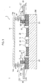
- FIG. 2 A schematic planar pattern configuration of the package 1 according to the first embodiment is expressed as shown in FIG. 2 . Also, a schematic cross-sectional structure taken in the line I-I of Fig. 2 is expressed as shown in FIG. 3 .
- a schematic cross-sectional structure taken in the line II-II of Fig. 2 is expressed as shown in Fig. 4
- a schematic cross-sectional structure taken in the line III-III of Fig. 2 is expressed as shown in Fig. 5
- a schematic cross-sectional structure taken in the line IV-IV of Fig. 2 is expressed as shown in FIG. 6 .
- a configuration example of the package 1 according to the first embodiment includes: the conductive base plate 200; the semiconductor device 24 disposed on the conductive base plate 200; the metal wall 16 which houses the semiconductor device 24 and is disposed on the conductive base plate 200; the through-holes 34 formed at both the input and output units of the metal wall 16; the lower layer feed through (20i and 20o) inserted into the through-hole 34, and disposed on the conductive base plate 200; and the upper layer feed through 22 disposed on the inside lower layer feed through 20i, and adhered to the sidewall of the metal wall 16.
- the outside lower layer feed through 20o is surrounded by the metal wall 16.
- the lengthwise overlap width between the metal wall 16 and the upper layer feed through 22 is expressed as ⁇ L2.
- the horizontal overlap width between the metal wall 16 and the inside lower layer feed through 20i is expressed as ⁇ L1.
- the upper layer feed through 22 is adhered to the sidewalls of the metal wall 16 with silver brazing, for example.
- the width size of the adhesion portion is about 0.5 mm, for example.
- the contact surface between the lower layer feed through (20i and 20o) and the metal wall 16 is also adhered with silver brazing, for example.
- the outside lower layer feed through 20o passes through the metal wall 16.
- the bottom surfaces of the lower layer feed through (20i and 20o) contacts the conductive base plate 200, and the side surface of the lower layer feed through (20i and 20o) contacts the metal wall 16.
- the package 1 includes: the input stripline 19a disposed on lower layer feed through (20i and 20o), in the input unit of the metal wall 16; and the output stripline 19b disposed on lower layer feed through (20i and 20o), in the output unit of the metal wall 16.
- the upper layer feed through 22 is disposed at the inside of the metal wall 16, and is adhered to the sidewall of the metal wall 16 in the internal wall of the metal wall 16 as mentioned above.
- an air gap is provided between the input stripline 19a and the metal wall 16. Since an air layer 23 is disposed between the top surface of the input stripline 19a, and the metal wall 16, reduction of impedance is avoidable.
- an air gap is provided between the output stripline 19b and the metal wall 16. Since an air layer 23 is disposed between the top surface of the output stripline 19b, and the metal wall 16, reduction of impedance is avoidable.
- the lower layer feed through (20i, 20o) includes the inside lower layer feed through 20i disposed at the inside of the metal wall 16, and the outside lower layer feed through 20o disposed at the outside of the metal wall 16.
- the width WL1 of the inside lower layer feed through 20i disposed along the lines of the metal wall 16 is wider than the width WL2 of the outside lower layer feed through 20o, as above-mentioned.
- the package 1 may include: an input circuit substrate 26 and an output circuit substrate 28 which are adjoining of the semiconductor device 24 and are disposed on the conductive base plate 200 surrounded by the metal wall 16; an input matching circuit 17 which is disposed on the input circuit substrate 26 and is connected to the input stripline 19a; an output matching circuit 18 which is disposed on the output circuit substrate 28 and is connected to the output stripline 19b; bonding wires 12 and 14 connect between the semiconductor device 24, and the input matching circuit 17 and the output matching circuit 18.
- bonding wires 12 and 14 connect between the semiconductor device 24, and the input matching circuit 17 and the output matching circuit 18.
- between the input stripline 19a and the input matching circuits 17 is connected by the bonding wire 11
- between the output stripline 19b and the output matching circuits 18 is connected by the bonding wire 15.
- the package 1 according to the first embodiment may include the metal seal ring 14a disposed on the metal wall 16, and the metal cap 10 disposed on the metal seal ring 14a.
- a high frequency terminal structure includes: the metal wall 10; the through-holes 34 formed at both the input and output units of the metal wall 16; the lower layer feed through (20i and 20o) inserted into the through-hole 34; and the upper layer feed through 22 disposed on the inside lower layer feed through 20i, and adhered to the sidewall of the metal wall 16.
- the outside lower layer feed through 20o is surrounded by the metal wall 16.
- the high frequency terminal structure according to the first embodiment may further include the input stripline 19a disposed on the lower layer feed through (20i and 20o) in the input unit of the metal wall 16, and the output stripline 19b disposed on the lower layer feed through (20i and 20o) in the output unit of the metal wall 16.
- each of the air layers 23 is formed at each of the top surfaces of the signal lines of the input stripline 19a and the output stripline 19b of the portion surrounded by the metal wall 16, respectively, and thereby reduction of impedance is avoidable. As a result, it can obtain the high frequency terminal structure whose impedance matching is satisfactory, reflection loss is controlled, and characteristics of the electric power capability is improved.
- a fabrication method for the package according to the first embodiment includes: forming the conductive base plate 200; forming the semiconductor device 24 on the conductive base plate 200; forming the metal wall 16 on the conductive base plate 200 to house the semiconductor device 24; forming the through-hole 34 at the input and output units of the metal wall 16; inserting the lower layer feed through (20i and 20o) into the through-hole 34 and forming the lower layer feed through (20i and 20o) on the conductive base plate 200; and forming the upper layer feed through 22 on the lower layer feed through 20i while adhering the upper layer feed through 22 to the sidewall of the metal wall 16.
- the metal wall 16 is formed so that the outside lower layer feed through 20o is surrounded.
- the fabrication method for the package according to the first embodiment may further include: forming the input stripline 19a on lower layer feed through (20i and 20o), in the input unit of the metal wall 16; and forming the output stripline 19b on lower layer feed through (20i and 20o), in the output unit of the metal wall 16.
- the upper layer feed through 22 is formed at the inside of the metal wall 16, and is adhered to the sidewall of the metal wall 16, in the internal wall of the metal wall 16.
- the fabrication method for the package according to the first embodiment may further include: forming the input circuit substrate 26 and the output circuit substrate 28 on the conductive base plate 200 surrounded by the metal wall 16 so as to adjoin the semiconductor device 24; forming the input matching circuit 17 connected to the input stripline 19a on the input circuit substrate 26; forming the output matching circuit 18 connected to the output stripline 19b on the output circuit substrate 28; and forming the bonding wires 12 and 14 for connecting the semiconductor device 24 with the input matching circuit 17 and the output matching circuit 18.
- the fabrication method for the package according to the first embodiment may further include: forming the metal seal ring 14a on the metal wall 16; and forming the metal cap 10 on the metal seal ring 14a.
- FIG. 7 A schematic planar pattern configuration showing by enlarging the feed through structure near the output terminal of the package 1 according to the first embodiment is expressed as shown in FIG. 7 . Also, a schematic cross-sectional structure taken in the line V-V of FIG. 7 is expressed as shown in FIG. 8 .
- WL1-WL2 2 ⁇ L1
- WL1 is the width of the inside lower layer feed through 20i disposed along the lines of the metal wall 16 in plane view
- WL2 is the width of the outside lower layer feed through 20o disposed along the lines of the metal wall 16 in plane view
- ⁇ L1 is the horizontal overlap width between the inside lower layer feed through 20i and the metal wall 16 in plane view, as mentioned above.
- ⁇ L2 is the lengthwise overlap width between the upper layer feed through 22 and the metal wall 16, in FIG. 8 .
- the outside lower layer feed through 20o is surrounded by the metal wall 16, and the upper layer feed through 22 is adhered to the sidewall of the metal wall 16, and thereby each of the air layers 23 is formed at each of the top surfaces of the signal lines of input stripline 19a and the output stripline 19b, respectively. Accordingly, reduction of impedance is avoided.
- the feed through structure (comparative example) by which each of the top surfaces of the signal lines of input stripline 19a and the output stripline 19b is surrounded by the metal outer wall
- the ratio of reduction of impedance is about 40% according to the comparative example, for example.
- the package 1 according to the first embodiment since each of the air layers 23 is formed at each of the top surfaces of the signal lines of input stripline 19a and the output stripline 19b of the portion surrounded by the metal wall 16, the reduction of impedance is avoidable. As a result, it can obtain the feed through structure whose impedance matching is satisfactory, reflection loss is controlled, and characteristics of electric power capability.
- the thickness W2 of the upper layer feed through 22 may be formed of the same grade or widely with (or than) the thickness W1 of the metal wall 16.
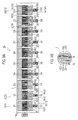
- FIG. 9A A schematic planar pattern configuration of the semiconductor device 24 which can be mounted on the package according to the first embodiment is expressed as shown in FIG. 9A , and an enlarged drawing of a part J of FIG. 9A is expressed as shown in FIG. 9B .
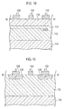
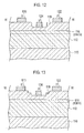
- configuration examples 1-4 of the semiconductor device 24 which can be mounted on the package according to the first embodiment, and schematic cross-sectional configuration examples 1-4 taken in the line II-II of FIG. 9B are expressed as shown in FIG. 10 to FIG. 13 , respectively.
- a plurality of FET cells FET 1 to FET 10 include: a semi-insulating substrate 110; a gate finger electrode 124, a source finger electrode 120, and a drain finger electrode 122 which are disposed on a first surface of the semi-insulating substrate 110, and have a plurality of fingers, respectively; a plurality of gate terminal electrodes G1, G2, ..., G10, a plurality of source terminal electrodes S11, S12, S21, S22, ..., S101, and S102 and the drain terminal electrodes D1, D2, ..., D10 which are disposed on the first surface of the semi-insulating substrate 110, and ties a plurality of fingers, respectively every the gate finger electrode 124, the source finger electrode 120, and the drain finger electrode 122; VIA holes SC11, SC12, SC21, SC22, ..., SC101, and SC102 disposed at the lower part of the source
- the bonding wire 12 is connected to the gate terminal electrodes G1, G2, ..., G10, as already shown in FIG. 2 , and the bonding wire 14 is connected to the drain terminal electrodes D1, D2, ..., D10.
- the source terminal electrodes S11, S12, S21, S22, ..., S101, and S102 are connected to the ground electrode (not shown), via the barrier metal layers (not shown) formed in the internal wall of the VIA holes SC11, SC12, SC21, SC22, ..., SC101 and SC102, and via the filling metal layers (not shown) formed on the barrier metal layers and filled up with the VIA holes.
- the semi-insulating substrate 110 is either of a GaAs substrate, an SiC substrate, a GaN substrate, a substrate in which a GaN epitaxial layer is formed on the SiC substrate, a substrate which a heterojunction epitaxial layer composed of GaN/AIGaN is formed on the SiC substrate, a sapphire substrate or a diamond substrate.
- FIG. 10 shows a High Electron Mobility Transistor (HEMT) as the constructional example 1.
- HEMT High Electron Mobility Transistor
- a constructional example 2 of an FET cell of the semiconductor device 24 which can be mounted in the package according to the first embodiment includes: a semi-insulating substrate 110; a nitride based compound semiconductor layer 112 disposed on the semi-insulating substrate 110; a source region 126 and a drain region 128 which are disposed on the nitride based compound semiconductor layer 112; and a source finger electrode (S) 120 disposed on the source region 126, a gate finger electrode (G) 124 disposed on the nitride based compound semiconductor layer 112, and a drain finger electrode (D) 122 disposed on the drain region 128.
- Schottky contact is formed in the interface between the nitride based compound semiconductor layer 112 and the gate finger electrode (G) 124.
- FIG. 11 shows a Metal Semiconductor Field Effect Transistor (MESFET) as the constructional example 2.
- MSFET Metal Semiconductor Field Effect Transistor
- FIG. 12 shows HEMT as the constructional example 3.
- FIG. 13 shows HEMT as the constructional example 4.
- the nitride based compound semiconductor layer 112 except an active area is electrically used as an inactivity isolation region.
- the active area is composed of the source finger electrode 120, the 2DEG layer 116 directly under the gate finger electrode 124 and the drain finger electrode 122, and the 2DEG layer 116 between the source finger electrode 120 and the gate finger electrode 124 and between the drain finger electrode 122 and the gate finger electrode 124.
- ion species nitrogen (N), argon (Ar), etc. are applicable, for example.
- the amount of dosage with the ion implantation is about 1x10 14 (ions/cm 2 ), for example, and accelerating energy is about 100 keV to 200 keV, for example.
- an insulating film for passivation (not shown) is formed.
- the insulating film it can be formed of a nitride film, an alumina (Al 2 O 3 ) film, an oxide film (Si0 2 ), an oxynitriding film (SiON), etc. deposited by a Plasma Enhanced Chemical Vapor Deposition (PECVD) method, for example.
- PECVD Plasma Enhanced Chemical Vapor Deposition
- the source finger electrode 120 and the drain finger electrode 122 are formed of Ti/Al etc., for example.
- the gate finger electrode 124 can be formed, for example of Ni/Au etc.
- the pattern length of the longitudinal direction of the gate finger electrode 124, the source finger electrode 120, and the drain finger electrode 122 is set up to be short as the operating frequency becomes higher such as the microwave/millimeter wave/submillimeter wave.
- the pattern length is about 25 ⁇ m to 50 ⁇ m.
- the width of the source finger electrode 120 is about 40 ⁇ m, for example, and the width of the source terminal electrode S11, S12, S21, S22, ..., S101, and S102 is about 100 ⁇ m, for example.
- the formation width of the VIA holes SC11, SC12, SC21, SC22, ..., SC101, and SC102 is about 10 ⁇ m to about 40 ⁇ m, for example.
- the air layer is formed between the top surface of the signal line of the portion surrounded by the metal wall and the metal wall, the reduction of impedance is avoidable. As a result, it can obtain the package whose impedance matching is satisfactory, reflection loss is controlled, and characteristics of the electric power resistance.
- the first embodiment can provide the high airtight package used for the microwave band semiconductor device and the fabrication method for such package, and the high frequency terminal structure.
- FIG. 14A shows a schematic configuration of a metal cap 10.
- FIG. 14B shows a schematic configuration of a metal seal ring 14a.
- FIG. 14C shows a schematic configuration of a metal wall 16.
- FIG. 14D shows a schematic configuration of a lower layer feed through (30i and 30o) on a conductive base plate 200 provided with a counter boring unit 40, an input stripline 19a and an output stripline 19b on the lower layer feed through (30i, and 30o), and an upper layer feed through 22 on the lower layer feed through 30i.
- a schematic planar pattern configuration of the package 1 according to the second embodiment is similarly expressed as FIG. 2 .
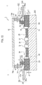
- FIG. 15 A schematic cross-sectional configuration of the package according to the second embodiment, and a schematic cross-sectional structure taken in the line I-I of FIG. 2 is expressed as shown in FIG. 15
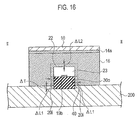
- a schematic cross-sectional structure taken in the line II-II of FIG. 2 is expressed as shown in FIG. 16
- a schematic cross-sectional structure taken in the line IV-IV of FIG. 2 is expressed as shown in FIG. 17 .
- the conductive base plate 200 includes the counter boring unit 40, and the lower layer feed through (30i and 30o) is disposed on the counter boring unit 40 of the conductive base plate 200.
- the counter boring depth ⁇ T of the counter boring unit 40 is about 0.1 mm to 0.5 mm, for example. Duplicating explanation is omitted since other configurations are the same as that of the package according to the first embodiment.
- the lower layer feed through (30i and 30o) can be disposed in the counter boring unit 40 by using the conductive base plate 200 including the counter boring unit 40, it can prevent the displacement between the convex feed-through 25 composed of the lower layer feed through (30i and 30o) and the upper layer feed through 22, and the metal wall 16.
- FIG. 9A and FIG. 9B An example of a schematic planar pattern configuration of the semiconductor device 24 which can be mounted in the package according to the second embodiment is similarly expressed as FIG. 9A and FIG. 9B . Also, configuration examples 1-4 of the semiconductor device 24 which can be mounted in the package according to the second embodiment are similarly expressed as FIG. 10 to FIG. 13 , respectively. Therefore, the duplicating explanation will be omitted.
- a high frequency terminal structure includes: the metal wall 16; the through-holes 34 formed at both the input and output units of the metal wall 16; the lower layer feed through (30i and 30o) inserted into the through-hole 34; and the upper layer feed through 22 disposed on the inside lower layer feed through 30i, and adhered to the sidewall of the metal wall 16.
- the outside lower layer feed through 30o is surrounded by the metal wall 16.
- the high frequency terminal structure according to the second embodiment may further include the input stripline 19a disposed on the lower layer feed through (30i and 30o) in the input unit of the metal wall 16, and the output stripline 19b disposed on the lower layer feed through (30i and 30o) in the output unit of the metal wall 16.
- each of the air layers 23 are formed at each of the top surfaces of the signal lines of the input stripline 19a and the output stripline 19b of the portion surrounded by the metal wall 16, respectively, and thereby reduction of impedance is avoidable. As a result, it can obtain the high frequency terminal structure whose impedance matching is satisfactory, reflection loss is controlled, and characteristics of the electric power resistance.
- a fabrication method for the package according to the second embodiment includes forming the counter boring unit 40 on the conductive base plate 200, as shown in FIG. 14 .
- the counter boring unit 40 can be formed by implementing dry etching or wet etching, for example to the conductive base plate 200.
- the counter boring unit 40 may be formed beforehand in the formation process of the conductive base plate 200.
- the step of forming the lower layer feed through (30i and 30o) includes forming the lower layer feed through (30i and 30o) on the counter boring unit 40 of the conductive base plate 200. Therefore, duplicating explanation is omitted since other steps are the same as that of the fabrication method for the package according to the first embodiment.
- the air layer is formed between the top surface of the signal line of the portion surrounded by the metal wall and the metal wall, the reduction of impedance is avoidable. As a result, it can obtain the package whose impedance matching is satisfactory, reflection loss is controlled, and characteristics of the electric power resistance.
- the second embodiment can provide the high airtight package which can prevent the displacement between the convex feed-through and the metal wall, by using the conductive base plate including the counter boring unit.
- it can provide the high airtight package used for the microwave band semiconductor device and the fabrication method for such package, and the high frequency terminal structure.
- the semiconductor device mounted in the package it needless to say that not only the FET and HEMT but also amplifying elements, such as a Laterally Diffused Metal-Oxide-Semiconductor Field Effect Transistor (LDMOS) and a Hetero-junction Bipolar Transistor (HBT), and a Micro Electro Mechanical Systems (MEMS) element, etc. are applicable.
- LDMOS Laterally Diffused Metal-Oxide-Semiconductor Field Effect Transistor
- HBT Hetero-junction Bipolar Transistor
- MEMS Micro Electro Mechanical Systems
Landscapes
- Junction Field-Effect Transistors (AREA)
- Led Device Packages (AREA)
- Structures Or Materials For Encapsulating Or Coating Semiconductor Devices Or Solid State Devices (AREA)
- Structure Of Printed Boards (AREA)
- Lead Frames For Integrated Circuits (AREA)
Applications Claiming Priority (1)
| Application Number | Priority Date | Filing Date | Title |
|---|---|---|---|
| JP2010258223 | 2010-11-18 |
Publications (3)
| Publication Number | Publication Date |
|---|---|
| EP2458630A2 true EP2458630A2 (fr) | 2012-05-30 |
| EP2458630A3 EP2458630A3 (fr) | 2013-08-07 |
| EP2458630B1 EP2458630B1 (fr) | 2016-10-12 |
Family
ID=45002548
Family Applications (1)
| Application Number | Title | Priority Date | Filing Date |
|---|---|---|---|
| EP11170561.2A Not-in-force EP2458630B1 (fr) | 2010-11-18 | 2011-06-20 | Conditionnement et structure de terminal haute fréquence pour celui-ci |
Country Status (4)
| Country | Link |
|---|---|
| US (1) | US8637873B2 (fr) |
| EP (1) | EP2458630B1 (fr) |
| JP (1) | JP5323167B2 (fr) |
| CN (1) | CN103117254B (fr) |
Cited By (2)
| Publication number | Priority date | Publication date | Assignee | Title |
|---|---|---|---|---|
| EP2595186A3 (fr) * | 2011-11-16 | 2013-08-14 | Kabushiki Kaisha Toshiba | Empaquetage pour semi-conducteur à haute fréquence |
| US9559056B2 (en) | 2014-09-18 | 2017-01-31 | Infineon Technologies Austria Ag | Electronic component |
Families Citing this family (11)
| Publication number | Priority date | Publication date | Assignee | Title |
|---|---|---|---|---|
| JP5913816B2 (ja) | 2011-02-21 | 2016-04-27 | 富士通株式会社 | 半導体装置の製造方法 |
| JP5851334B2 (ja) * | 2012-05-08 | 2016-02-03 | 株式会社東芝 | 高周波半導体用パッケージ |
| JP2014207389A (ja) | 2013-04-15 | 2014-10-30 | 株式会社東芝 | 半導体パッケージ |
| JP2014207388A (ja) | 2013-04-15 | 2014-10-30 | 株式会社東芝 | 半導体パッケージ |
| JP6219156B2 (ja) * | 2013-12-18 | 2017-10-25 | 日本ピラー工業株式会社 | アンテナ用ユニット |
| JP2015173234A (ja) | 2014-03-12 | 2015-10-01 | 株式会社東芝 | 高周波半導体装置用パッケージおよびその製造方法、並びに高周波半導体装置 |
| US10196745B2 (en) * | 2014-10-31 | 2019-02-05 | General Electric Company | Lid and method for sealing a non-magnetic package |
| JP6717519B2 (ja) * | 2015-11-16 | 2020-07-01 | 住友電工デバイス・イノベーション株式会社 | 半導体装置の製造方法 |
| WO2018078680A1 (fr) * | 2016-10-24 | 2018-05-03 | 三菱電機株式会社 | Dispositif à semiconducteur |
| CN110444511A (zh) * | 2019-07-23 | 2019-11-12 | 中国科学技术大学 | 提高超导量子处理器谐振频率的封装盒体结构 |
| CN111933585A (zh) * | 2020-07-23 | 2020-11-13 | 合肥圣达电子科技实业有限公司 | 一种高导热微波tr组件封装外壳及其加工方法 |
Family Cites Families (13)
| Publication number | Priority date | Publication date | Assignee | Title |
|---|---|---|---|---|
| JPS58190046A (ja) * | 1982-04-30 | 1983-11-05 | Fujitsu Ltd | 半導体装置 |
| FR2538617B1 (fr) | 1982-12-28 | 1986-02-28 | Thomson Csf | Boitier d'encapsulation pour semiconducteur de puissance, a isolement entree-sortie ameliore |
| JPH03268618A (ja) | 1990-03-19 | 1991-11-29 | Fuji Electric Co Ltd | フィルタ可変機能付伝送装置 |
| JPH0480101U (fr) * | 1990-11-26 | 1992-07-13 | ||
| JP3441192B2 (ja) | 1994-09-28 | 2003-08-25 | 新光電気工業株式会社 | 電子部品用メタルパッケージ |
| JP3268618B2 (ja) | 1994-11-24 | 2002-03-25 | 株式会社リコー | 画像支持体再生装置 |
| JP3515886B2 (ja) | 1997-09-29 | 2004-04-05 | 三菱電機株式会社 | 半導体装置およびその製造方法 |
| JPH11238823A (ja) * | 1998-02-23 | 1999-08-31 | Toshiba Corp | 半導体パッケージ |
| JP3336982B2 (ja) | 1998-12-16 | 2002-10-21 | 松下電器産業株式会社 | 半導体装置およびその製造方法 |
| JP3829839B2 (ja) * | 2003-11-14 | 2006-10-04 | 三菱電機株式会社 | 高周波パッケージ |
| JP4519637B2 (ja) | 2004-12-28 | 2010-08-04 | 株式会社東芝 | 半導体装置 |
| JP4836760B2 (ja) * | 2006-11-28 | 2011-12-14 | 京セラ株式会社 | 接続端子ならびにこれを用いた電子部品収納用パッケージおよび電子装置 |
| JP5806464B2 (ja) * | 2010-02-03 | 2015-11-10 | 株式会社東芝 | 半導体素子収納用パッケージ及びそれを用いた半導体装置 |
-
2011
- 2011-06-20 EP EP11170561.2A patent/EP2458630B1/fr not_active Not-in-force
- 2011-06-20 US US13/164,155 patent/US8637873B2/en not_active Expired - Fee Related
- 2011-11-16 JP JP2011250469A patent/JP5323167B2/ja not_active Expired - Fee Related
-
2012
- 2012-04-28 CN CN201210130267.3A patent/CN103117254B/zh not_active Expired - Fee Related
Non-Patent Citations (1)
| Title |
|---|
| None |
Cited By (3)
| Publication number | Priority date | Publication date | Assignee | Title |
|---|---|---|---|---|
| EP2595186A3 (fr) * | 2011-11-16 | 2013-08-14 | Kabushiki Kaisha Toshiba | Empaquetage pour semi-conducteur à haute fréquence |
| EP3190615A1 (fr) * | 2011-11-16 | 2017-07-12 | Kabushiki Kaisha Toshiba | Embpaquetage semi-conducteur à haute fréquence |
| US9559056B2 (en) | 2014-09-18 | 2017-01-31 | Infineon Technologies Austria Ag | Electronic component |
Also Published As
| Publication number | Publication date |
|---|---|
| JP2012124477A (ja) | 2012-06-28 |
| EP2458630B1 (fr) | 2016-10-12 |
| EP2458630A3 (fr) | 2013-08-07 |
| JP5323167B2 (ja) | 2013-10-23 |
| US20120126246A1 (en) | 2012-05-24 |
| US8637873B2 (en) | 2014-01-28 |
| CN103117254B (zh) | 2015-09-30 |
| CN103117254A (zh) | 2013-05-22 |
Similar Documents
| Publication | Publication Date | Title |
|---|---|---|
| EP2458630B1 (fr) | Conditionnement et structure de terminal haute fréquence pour celui-ci | |
| JP5450313B2 (ja) | 高周波半導体用パッケージおよびその作製方法 | |
| US8471382B2 (en) | Package and high frequency terminal structure for the same | |
| TWI469275B (zh) | Package | |
| JP2012178525A (ja) | パッケージ | |
| JP2012038837A (ja) | パッケージおよびその作製方法 | |
| EP2463906B1 (fr) | Dispositif semi-conducteur | |
| US7990223B1 (en) | High frequency module and operating method of the same | |
| JP2012182306A (ja) | Mmic用パッケージ | |
| JP2012182386A (ja) | パッケージ | |
| JP5851334B2 (ja) | 高周波半導体用パッケージ | |
| JP5843703B2 (ja) | 高周波半導体用パッケージ | |
| JP5513991B2 (ja) | 高周波モジュールおよびその動作方法 | |
| JP2012209334A (ja) | ミリ波帯用薄型パッケージおよびその製造方法 | |
| JP5734727B2 (ja) | 半導体装置 | |
| JP5562898B2 (ja) | 半導体装置およびその製造方法 | |
| JP2012146910A (ja) | 半導体装置 | |
| JP2012146728A (ja) | パッケージ | |
| JP5892770B2 (ja) | 高周波半導体装置 | |
| JP2011250360A (ja) | 高周波モジュール | |
| JP2011238842A (ja) | 高周波半導体装置およびその製造方法 | |
| JP2011238648A (ja) | 高出力用半導体パッケージおよびその作製方法 | |
| JP2013118571A (ja) | パッケージ装置 |
Legal Events
| Date | Code | Title | Description |
|---|---|---|---|
| PUAI | Public reference made under article 153(3) epc to a published international application that has entered the european phase |
Free format text: ORIGINAL CODE: 0009012 |
|
| 17P | Request for examination filed |
Effective date: 20110620 |
|
| AK | Designated contracting states |
Kind code of ref document: A2 Designated state(s): AL AT BE BG CH CY CZ DE DK EE ES FI FR GB GR HR HU IE IS IT LI LT LU LV MC MK MT NL NO PL PT RO RS SE SI SK SM TR |
|
| AX | Request for extension of the european patent |
Extension state: BA ME |
|
| PUAL | Search report despatched |
Free format text: ORIGINAL CODE: 0009013 |
|
| AK | Designated contracting states |
Kind code of ref document: A3 Designated state(s): AL AT BE BG CH CY CZ DE DK EE ES FI FR GB GR HR HU IE IS IT LI LT LU LV MC MK MT NL NO PL PT RO RS SE SI SK SM TR |
|
| AX | Request for extension of the european patent |
Extension state: BA ME |
|
| RIC1 | Information provided on ipc code assigned before grant |
Ipc: H01L 29/417 20060101ALI20130702BHEP Ipc: H01L 23/66 20060101ALI20130702BHEP Ipc: H01L 23/047 20060101AFI20130702BHEP |
|
| GRAP | Despatch of communication of intention to grant a patent |
Free format text: ORIGINAL CODE: EPIDOSNIGR1 |
|
| INTG | Intention to grant announced |
Effective date: 20160502 |
|
| GRAS | Grant fee paid |
Free format text: ORIGINAL CODE: EPIDOSNIGR3 |
|
| GRAA | (expected) grant |
Free format text: ORIGINAL CODE: 0009210 |
|
| AK | Designated contracting states |
Kind code of ref document: B1 Designated state(s): AL AT BE BG CH CY CZ DE DK EE ES FI FR GB GR HR HU IE IS IT LI LT LU LV MC MK MT NL NO PL PT RO RS SE SI SK SM TR |
|
| REG | Reference to a national code |
Ref country code: GB Ref legal event code: FG4D |
|
| REG | Reference to a national code |
Ref country code: CH Ref legal event code: EP |
|
| REG | Reference to a national code |
Ref country code: AT Ref legal event code: REF Ref document number: 837182 Country of ref document: AT Kind code of ref document: T Effective date: 20161015 |
|
| REG | Reference to a national code |
Ref country code: IE Ref legal event code: FG4D |
|
| REG | Reference to a national code |
Ref country code: DE Ref legal event code: R096 Ref document number: 602011031130 Country of ref document: DE |
|
| REG | Reference to a national code |
Ref country code: LT Ref legal event code: MG4D |
|
| REG | Reference to a national code |
Ref country code: NL Ref legal event code: MP Effective date: 20161012 |
|
| PG25 | Lapsed in a contracting state [announced via postgrant information from national office to epo] |
Ref country code: LV Free format text: LAPSE BECAUSE OF FAILURE TO SUBMIT A TRANSLATION OF THE DESCRIPTION OR TO PAY THE FEE WITHIN THE PRESCRIBED TIME-LIMIT Effective date: 20161012 |
|
| REG | Reference to a national code |
Ref country code: AT Ref legal event code: MK05 Ref document number: 837182 Country of ref document: AT Kind code of ref document: T Effective date: 20161012 |
|
| PG25 | Lapsed in a contracting state [announced via postgrant information from national office to epo] |
Ref country code: GR Free format text: LAPSE BECAUSE OF FAILURE TO SUBMIT A TRANSLATION OF THE DESCRIPTION OR TO PAY THE FEE WITHIN THE PRESCRIBED TIME-LIMIT Effective date: 20170113 Ref country code: SE Free format text: LAPSE BECAUSE OF FAILURE TO SUBMIT A TRANSLATION OF THE DESCRIPTION OR TO PAY THE FEE WITHIN THE PRESCRIBED TIME-LIMIT Effective date: 20161012 Ref country code: NO Free format text: LAPSE BECAUSE OF FAILURE TO SUBMIT A TRANSLATION OF THE DESCRIPTION OR TO PAY THE FEE WITHIN THE PRESCRIBED TIME-LIMIT Effective date: 20170112 Ref country code: LT Free format text: LAPSE BECAUSE OF FAILURE TO SUBMIT A TRANSLATION OF THE DESCRIPTION OR TO PAY THE FEE WITHIN THE PRESCRIBED TIME-LIMIT Effective date: 20161012 |
|
| REG | Reference to a national code |
Ref country code: FR Ref legal event code: PLFP Year of fee payment: 7 |
|
| PG25 | Lapsed in a contracting state [announced via postgrant information from national office to epo] |
Ref country code: ES Free format text: LAPSE BECAUSE OF FAILURE TO SUBMIT A TRANSLATION OF THE DESCRIPTION OR TO PAY THE FEE WITHIN THE PRESCRIBED TIME-LIMIT Effective date: 20161012 Ref country code: PT Free format text: LAPSE BECAUSE OF FAILURE TO SUBMIT A TRANSLATION OF THE DESCRIPTION OR TO PAY THE FEE WITHIN THE PRESCRIBED TIME-LIMIT Effective date: 20170213 Ref country code: PL Free format text: LAPSE BECAUSE OF FAILURE TO SUBMIT A TRANSLATION OF THE DESCRIPTION OR TO PAY THE FEE WITHIN THE PRESCRIBED TIME-LIMIT Effective date: 20161012 Ref country code: FI Free format text: LAPSE BECAUSE OF FAILURE TO SUBMIT A TRANSLATION OF THE DESCRIPTION OR TO PAY THE FEE WITHIN THE PRESCRIBED TIME-LIMIT Effective date: 20161012 Ref country code: HR Free format text: LAPSE BECAUSE OF FAILURE TO SUBMIT A TRANSLATION OF THE DESCRIPTION OR TO PAY THE FEE WITHIN THE PRESCRIBED TIME-LIMIT Effective date: 20161012 Ref country code: BE Free format text: LAPSE BECAUSE OF FAILURE TO SUBMIT A TRANSLATION OF THE DESCRIPTION OR TO PAY THE FEE WITHIN THE PRESCRIBED TIME-LIMIT Effective date: 20161012 Ref country code: IS Free format text: LAPSE BECAUSE OF FAILURE TO SUBMIT A TRANSLATION OF THE DESCRIPTION OR TO PAY THE FEE WITHIN THE PRESCRIBED TIME-LIMIT Effective date: 20170212 Ref country code: RS Free format text: LAPSE BECAUSE OF FAILURE TO SUBMIT A TRANSLATION OF THE DESCRIPTION OR TO PAY THE FEE WITHIN THE PRESCRIBED TIME-LIMIT Effective date: 20161012 Ref country code: AT Free format text: LAPSE BECAUSE OF FAILURE TO SUBMIT A TRANSLATION OF THE DESCRIPTION OR TO PAY THE FEE WITHIN THE PRESCRIBED TIME-LIMIT Effective date: 20161012 Ref country code: NL Free format text: LAPSE BECAUSE OF FAILURE TO SUBMIT A TRANSLATION OF THE DESCRIPTION OR TO PAY THE FEE WITHIN THE PRESCRIBED TIME-LIMIT Effective date: 20161012 |
|
| REG | Reference to a national code |
Ref country code: DE Ref legal event code: R097 Ref document number: 602011031130 Country of ref document: DE |
|
| PG25 | Lapsed in a contracting state [announced via postgrant information from national office to epo] |
Ref country code: SK Free format text: LAPSE BECAUSE OF FAILURE TO SUBMIT A TRANSLATION OF THE DESCRIPTION OR TO PAY THE FEE WITHIN THE PRESCRIBED TIME-LIMIT Effective date: 20161012 Ref country code: DK Free format text: LAPSE BECAUSE OF FAILURE TO SUBMIT A TRANSLATION OF THE DESCRIPTION OR TO PAY THE FEE WITHIN THE PRESCRIBED TIME-LIMIT Effective date: 20161012 Ref country code: RO Free format text: LAPSE BECAUSE OF FAILURE TO SUBMIT A TRANSLATION OF THE DESCRIPTION OR TO PAY THE FEE WITHIN THE PRESCRIBED TIME-LIMIT Effective date: 20161012 Ref country code: EE Free format text: LAPSE BECAUSE OF FAILURE TO SUBMIT A TRANSLATION OF THE DESCRIPTION OR TO PAY THE FEE WITHIN THE PRESCRIBED TIME-LIMIT Effective date: 20161012 Ref country code: CZ Free format text: LAPSE BECAUSE OF FAILURE TO SUBMIT A TRANSLATION OF THE DESCRIPTION OR TO PAY THE FEE WITHIN THE PRESCRIBED TIME-LIMIT Effective date: 20161012 |
|
| PGFP | Annual fee paid to national office [announced via postgrant information from national office to epo] |
Ref country code: GB Payment date: 20170614 Year of fee payment: 7 Ref country code: DE Payment date: 20170613 Year of fee payment: 7 Ref country code: FR Payment date: 20170511 Year of fee payment: 7 |
|
| PLBE | No opposition filed within time limit |
Free format text: ORIGINAL CODE: 0009261 |
|
| STAA | Information on the status of an ep patent application or granted ep patent |
Free format text: STATUS: NO OPPOSITION FILED WITHIN TIME LIMIT |
|
| PG25 | Lapsed in a contracting state [announced via postgrant information from national office to epo] |
Ref country code: SM Free format text: LAPSE BECAUSE OF FAILURE TO SUBMIT A TRANSLATION OF THE DESCRIPTION OR TO PAY THE FEE WITHIN THE PRESCRIBED TIME-LIMIT Effective date: 20161012 Ref country code: BG Free format text: LAPSE BECAUSE OF FAILURE TO SUBMIT A TRANSLATION OF THE DESCRIPTION OR TO PAY THE FEE WITHIN THE PRESCRIBED TIME-LIMIT Effective date: 20170112 Ref country code: IT Free format text: LAPSE BECAUSE OF FAILURE TO SUBMIT A TRANSLATION OF THE DESCRIPTION OR TO PAY THE FEE WITHIN THE PRESCRIBED TIME-LIMIT Effective date: 20161012 |
|
| 26N | No opposition filed |
Effective date: 20170713 |
|
| PG25 | Lapsed in a contracting state [announced via postgrant information from national office to epo] |
Ref country code: SI Free format text: LAPSE BECAUSE OF FAILURE TO SUBMIT A TRANSLATION OF THE DESCRIPTION OR TO PAY THE FEE WITHIN THE PRESCRIBED TIME-LIMIT Effective date: 20161012 |
|
| PG25 | Lapsed in a contracting state [announced via postgrant information from national office to epo] |
Ref country code: MC Free format text: LAPSE BECAUSE OF FAILURE TO SUBMIT A TRANSLATION OF THE DESCRIPTION OR TO PAY THE FEE WITHIN THE PRESCRIBED TIME-LIMIT Effective date: 20161012 |
|
| REG | Reference to a national code |
Ref country code: CH Ref legal event code: PL |
|
| REG | Reference to a national code |
Ref country code: IE Ref legal event code: MM4A |
|
| PG25 | Lapsed in a contracting state [announced via postgrant information from national office to epo] |
Ref country code: LU Free format text: LAPSE BECAUSE OF NON-PAYMENT OF DUE FEES Effective date: 20170620 Ref country code: IE Free format text: LAPSE BECAUSE OF NON-PAYMENT OF DUE FEES Effective date: 20170620 Ref country code: CH Free format text: LAPSE BECAUSE OF NON-PAYMENT OF DUE FEES Effective date: 20170630 Ref country code: LI Free format text: LAPSE BECAUSE OF NON-PAYMENT OF DUE FEES Effective date: 20170630 |
|
| PG25 | Lapsed in a contracting state [announced via postgrant information from national office to epo] |
Ref country code: MT Free format text: LAPSE BECAUSE OF NON-PAYMENT OF DUE FEES Effective date: 20170620 |
|
| REG | Reference to a national code |
Ref country code: DE Ref legal event code: R119 Ref document number: 602011031130 Country of ref document: DE |
|
| GBPC | Gb: european patent ceased through non-payment of renewal fee |
Effective date: 20180620 |
|
| PG25 | Lapsed in a contracting state [announced via postgrant information from national office to epo] |
Ref country code: DE Free format text: LAPSE BECAUSE OF NON-PAYMENT OF DUE FEES Effective date: 20190101 Ref country code: GB Free format text: LAPSE BECAUSE OF NON-PAYMENT OF DUE FEES Effective date: 20180620 Ref country code: FR Free format text: LAPSE BECAUSE OF NON-PAYMENT OF DUE FEES Effective date: 20180630 |
|
| PG25 | Lapsed in a contracting state [announced via postgrant information from national office to epo] |
Ref country code: HU Free format text: LAPSE BECAUSE OF FAILURE TO SUBMIT A TRANSLATION OF THE DESCRIPTION OR TO PAY THE FEE WITHIN THE PRESCRIBED TIME-LIMIT; INVALID AB INITIO Effective date: 20110620 |
|
| PG25 | Lapsed in a contracting state [announced via postgrant information from national office to epo] |
Ref country code: CY Free format text: LAPSE BECAUSE OF NON-PAYMENT OF DUE FEES Effective date: 20161012 |
|
| PG25 | Lapsed in a contracting state [announced via postgrant information from national office to epo] |
Ref country code: MK Free format text: LAPSE BECAUSE OF FAILURE TO SUBMIT A TRANSLATION OF THE DESCRIPTION OR TO PAY THE FEE WITHIN THE PRESCRIBED TIME-LIMIT Effective date: 20161012 |
|
| PG25 | Lapsed in a contracting state [announced via postgrant information from national office to epo] |
Ref country code: TR Free format text: LAPSE BECAUSE OF FAILURE TO SUBMIT A TRANSLATION OF THE DESCRIPTION OR TO PAY THE FEE WITHIN THE PRESCRIBED TIME-LIMIT Effective date: 20161012 |
|
| PG25 | Lapsed in a contracting state [announced via postgrant information from national office to epo] |
Ref country code: AL Free format text: LAPSE BECAUSE OF FAILURE TO SUBMIT A TRANSLATION OF THE DESCRIPTION OR TO PAY THE FEE WITHIN THE PRESCRIBED TIME-LIMIT Effective date: 20161012 |